

 ATmega48/88/168
2. Overview
The ATmega48/88/168 is a low-power CMOS 8-bit microcontroller based on the AVR enhanced RISC architecture. By executing powerful instructions in a single clock cycle, the ATmega48/88/168 achieves throughputs approaching 1 MIPS per MHz allowing the system designer to optimize power consumption versus processing speed.
2.1Block Diagram
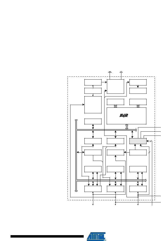
Figure 2-1.
Block Diagram
|
|
GND |
VCC |
|
|
|
Watchdog |
|
Power |
debugWIRE |
|
|
Timer |
|
|
||
|
Supervision |
|
|
||
|
|
|
|
||
|
Watchdog |
POR / BOD & |
PROGRAM |
|
|
|
|
RESET |
|
||
|
Oscillator |
|
LOGIC |
|
|
|
|
|
|
||
|
Oscillator |
|
Flash |
SRAM |
|
|
Circuits / |
|
|
||
|
|
|
|
|
|
|
Clock |
|
|
|
|
|
Generation |
|
|
|
|
|
|
|
|
CPU |
|
|
EEPROM |
|
|
|
|
|
|
|
|
|
AVCC |
|
|
|
|
|
AREF |
|
|
|
|
|
GND |
|
8bit T/C 0 |
16bit T/C 1 |
A/D Conv. |
2 |
|
|
|
||||
DATABUS |
8bit T/C 2 |
|
Analog |
Internal |
6 |
|
Comp. |
Bandgap |
|||
|
|
|
|||
|
|
|
|
|
|
|
USART 0 |
|
SPI |
TWI |
|
|
PORT D (8) |
PORT B (8) |
PORT C (7) |
|
|
|
|
|
|
|
RESET |
|
|
|
|
|
XTAL[1..2] |
|
PD[0..7] |
|
PB[0..7] |
PC[0..6] |
ADC[6..7] |
The AVR core combines a rich instruction set with 32 general purpose working registers. All the 32 registers are directly connected to the Arithmetic Logic Unit (ALU), allowing two independent registers to be accessed in one single instruction executed in one clock cycle. The resulting
5
2545M–AVR–09/07

architecture is more code efficient while achieving throughputs up to ten times faster than conventional CISC microcontrollers.
The ATmega48/88/168 provides the following features: 4K/8K/16K bytes of In-System Programmable Flash with Read-While-Write capabilities, 256/512/512 bytes EEPROM, 512/1K/1K bytes SRAM, 23 general purpose I/O lines, 32 general purpose working registers, three flexible Timer/Counters with compare modes, internal and external interrupts, a serial programmable USART, a byte-oriented 2-wire Serial Interface, an SPI serial port, a 6-channel 10-bit ADC (8 channels in TQFP and QFN/MLF packages), a programmable Watchdog Timer with internal Oscillator, and five software selectable power saving modes. The Idle mode stops the CPU while allowing the SRAM, Timer/Counters, USART, 2-wire Serial Interface, SPI port, and interrupt system to continue functioning. The Power-down mode saves the register contents but freezes the Oscillator, disabling all other chip functions until the next interrupt or hardware reset. In Power-save mode, the asynchronous timer continues to run, allowing the user to maintain a timer base while the rest of the device is sleeping. The ADC Noise Reduction mode stops the CPU and all I/O modules except asynchronous timer and ADC, to minimize switching noise during ADC conversions. In Standby mode, the crystal/resonator Oscillator is running while the rest of the device is sleeping. This allows very fast start-up combined with low power consumption.
The device is manufactured using Atmel’s high density non-volatile memory technology. The On-chip ISP Flash allows the program memory to be reprogrammed In-System through an SPI serial interface, by a conventional non-volatile memory programmer, or by an On-chip Boot program running on the AVR core. The Boot program can use any interface to download the application program in the Application Flash memory. Software in the Boot Flash section will continue to run while the Application Flash section is updated, providing true Read-While-Write operation. By combining an 8-bit RISC CPU with In-System Self-Programmable Flash on a monolithic chip, the Atmel ATmega48/88/168 is a powerful microcontroller that provides a highly flexible and cost effective solution to many embedded control applications.
The ATmega48/88/168 AVR is supported with a full suite of program and system development tools including: C Compilers, Macro Assemblers, Program Debugger/Simulators, In-Circuit Emulators, and Evaluation kits.
2.2Comparison Between ATmega48, ATmega88, and ATmega168
The ATmega48, ATmega88 and ATmega168 differ only in memory sizes, boot loader support, and interrupt vector sizes. Table 2-1 summarizes the different memory and interrupt vector sizes for the three devices.
Table 2-1. |
Memory Size Summary |
|
|
||
Device |
|
Flash |
EEPROM |
RAM |
Interrupt Vector Size |
|
|
|
|
|
|
ATmega48 |
|
4K Bytes |
256 Bytes |
512 Bytes |
1 instruction word/vector |
|
|
|
|
|
|
ATmega88 |
|
8K Bytes |
512 Bytes |
1K Bytes |
1 instruction word/vector |
|
|
|
|
|
|
ATmega168 |
|
16K Bytes |
512 Bytes |
1K Bytes |
2 instruction words/vector |
|
|
|
|
|
|
ATmega88 and ATmega168 support a real Read-While-Write Self-Programming mechanism.
There is a separate Boot Loader Section, and the SPM instruction can only execute from there.
In ATmega48, there is no Read-While-Write support and no separate Boot Loader Section. The
SPM instruction can execute from the entire Flash.
6 ATmega48/88/168 
2545M–AVR–09/07