

- •Features
- •1. Pin Configurations
- •1.1 Pin Descriptions
- •1.1.3 Port B (PB7:0) XTAL1/XTAL2/TOSC1/TOSC2
- •1.1.4 Port C (PC5:0)
- •1.1.5 PC6/RESET
- •1.1.6 Port D (PD7:0)
- •1.1.8 AREF
- •1.1.9 ADC7:6 (TQFP and QFN/MLF Package Only)
- •2. Overview
- •2.1 Block Diagram
- •2.2 Comparison Between ATmega48, ATmega88, and ATmega168
- •3. Resources
- •4. Data Retention
- •5. About Code Examples
- •6. AVR CPU Core
- •6.1 Overview
- •6.2 Architectural Overview
- •6.4 Status Register
- •6.5 General Purpose Register File
- •6.6 Stack Pointer
- •6.7 Instruction Execution Timing
- •6.8 Reset and Interrupt Handling
- •6.8.1 Interrupt Response Time
- •7. AVR Memories
- •7.1 Overview
- •7.3 SRAM Data Memory
- •7.3.1 Data Memory Access Times
- •7.4 EEPROM Data Memory
- •7.4.1 EEPROM Read/Write Access
- •7.4.2 Preventing EEPROM Corruption
- •7.5 I/O Memory
- •7.5.1 General Purpose I/O Registers
- •7.6 Register Description
- •8. System Clock and Clock Options
- •8.1 Clock Systems and their Distribution
- •8.2 Clock Sources
- •8.2.1 Default Clock Source
- •8.2.2 Clock Startup Sequence
- •8.3 Low Power Crystal Oscillator
- •8.4 Full Swing Crystal Oscillator
- •8.5 Low Frequency Crystal Oscillator
- •8.6 Calibrated Internal RC Oscillator
- •8.7 128 kHz Internal Oscillator
- •8.8 External Clock
- •8.9 Clock Output Buffer
- •8.10 Timer/Counter Oscillator
- •8.11 System Clock Prescaler
- •8.12 Register Description
- •9. Power Management and Sleep Modes
- •9.1 Sleep Modes
- •9.2 Idle Mode
- •9.3 ADC Noise Reduction Mode
- •9.4 Power-down Mode
- •9.5 Power-save Mode
- •9.6 Standby Mode
- •9.7 Power Reduction Register
- •9.8 Minimizing Power Consumption
- •9.8.1 Analog to Digital Converter
- •9.8.2 Analog Comparator
- •9.8.4 Internal Voltage Reference
- •9.8.5 Watchdog Timer
- •9.8.6 Port Pins
- •9.9 Register Description
- •10. System Control and Reset
- •10.1 Resetting the AVR
- •10.2 Reset Sources
- •10.3 Power-on Reset
- •10.4 External Reset
- •10.6 Watchdog System Reset
- •10.7 Internal Voltage Reference
- •10.8 Watchdog Timer
- •10.8.1 Features
- •10.9 Register Description
- •11. Interrupts
- •11.1 Overview
- •11.2 Interrupt Vectors in ATmega48
- •11.3 Interrupt Vectors in ATmega88
- •11.4 Interrupt Vectors in ATmega168
- •11.4.1 Moving Interrupts Between Application and Boot Space, ATmega88 and ATmega168
- •11.5 Register Description
- •12. External Interrupts
- •12.1 Pin Change Interrupt Timing
- •12.2 Register Description
- •13. I/O-Ports
- •13.1 Overview
- •13.2 Ports as General Digital I/O
- •13.2.1 Configuring the Pin
- •13.2.2 Toggling the Pin
- •13.2.3 Switching Between Input and Output
- •13.2.4 Reading the Pin Value
- •13.2.5 Digital Input Enable and Sleep Modes
- •13.2.6 Unconnected Pins
- •13.3 Alternate Port Functions
- •13.3.1 Alternate Functions of Port B
- •13.3.2 Alternate Functions of Port C
- •13.3.3 Alternate Functions of Port D
- •13.4 Register Description
- •14. 8-bit Timer/Counter0 with PWM
- •14.1 Features
- •14.2 Overview
- •14.2.1 Definitions
- •14.2.2 Registers
- •14.3 Timer/Counter Clock Sources
- •14.4 Counter Unit
- •14.5 Output Compare Unit
- •14.5.1 Force Output Compare
- •14.5.2 Compare Match Blocking by TCNT0 Write
- •14.5.3 Using the Output Compare Unit
- •14.6 Compare Match Output Unit
- •14.6.1 Compare Output Mode and Waveform Generation
- •14.7 Modes of Operation
- •14.7.1 Normal Mode
- •14.7.2 Clear Timer on Compare Match (CTC) Mode
- •14.7.3 Fast PWM Mode
- •14.7.4 Phase Correct PWM Mode
- •14.8 Timer/Counter Timing Diagrams
- •14.9 Register Description
- •15. 16-bit Timer/Counter1 with PWM
- •15.1 Features
- •15.2 Overview
- •15.2.1 Registers
- •15.2.2 Definitions
- •15.3.1 Reusing the Temporary High Byte Register
- •15.4 Timer/Counter Clock Sources
- •15.5 Counter Unit
- •15.6 Input Capture Unit
- •15.6.1 Input Capture Trigger Source
- •15.6.2 Noise Canceler
- •15.6.3 Using the Input Capture Unit
- •15.7 Output Compare Units
- •15.7.1 Force Output Compare
- •15.7.2 Compare Match Blocking by TCNT1 Write
- •15.7.3 Using the Output Compare Unit
- •15.8 Compare Match Output Unit
- •15.8.1 Compare Output Mode and Waveform Generation
- •15.9 Modes of Operation
- •15.9.1 Normal Mode
- •15.9.2 Clear Timer on Compare Match (CTC) Mode
- •15.9.3 Fast PWM Mode
- •15.9.4 Phase Correct PWM Mode
- •15.9.5 Phase and Frequency Correct PWM Mode
- •15.10 Timer/Counter Timing Diagrams
- •15.11 Register Description
- •16. Timer/Counter0 and Timer/Counter1 Prescalers
- •16.0.1 Internal Clock Source
- •16.0.2 Prescaler Reset
- •16.0.3 External Clock Source
- •16.1 Register Description
- •17. 8-bit Timer/Counter2 with PWM and Asynchronous Operation
- •17.1 Features
- •17.2 Overview
- •17.2.1 Registers
- •17.2.2 Definitions
- •17.3 Timer/Counter Clock Sources
- •17.4 Counter Unit
- •17.5 Output Compare Unit
- •17.5.1 Force Output Compare
- •17.5.2 Compare Match Blocking by TCNT2 Write
- •17.5.3 Using the Output Compare Unit
- •17.6 Compare Match Output Unit
- •17.6.1 Compare Output Mode and Waveform Generation
- •17.7 Modes of Operation
- •17.7.1 Normal Mode
- •17.7.2 Clear Timer on Compare Match (CTC) Mode
- •17.7.3 Fast PWM Mode
- •17.7.4 Phase Correct PWM Mode
- •17.8 Timer/Counter Timing Diagrams
- •17.9 Asynchronous Operation of Timer/Counter2
- •17.10 Timer/Counter Prescaler
- •17.11 Register Description
- •18.1 Features
- •18.2 Overview
- •18.3 SS Pin Functionality
- •18.3.1 Slave Mode
- •18.3.2 Master Mode
- •18.4 Data Modes
- •18.5 Register Description
- •19. USART0
- •19.1 Features
- •19.2 Overview
- •19.3 Clock Generation
- •19.3.2 Double Speed Operation (U2Xn)
- •19.3.3 External Clock
- •19.3.4 Synchronous Clock Operation
- •19.4 Frame Formats
- •19.4.1 Parity Bit Calculation
- •19.5 USART Initialization
- •19.6.1 Sending Frames with 5 to 8 Data Bit
- •19.6.2 Sending Frames with 9 Data Bit
- •19.6.3 Transmitter Flags and Interrupts
- •19.6.4 Parity Generator
- •19.6.5 Disabling the Transmitter
- •19.7.1 Receiving Frames with 5 to 8 Data Bits
- •19.7.2 Receiving Frames with 9 Data Bits
- •19.7.3 Receive Compete Flag and Interrupt
- •19.7.4 Receiver Error Flags
- •19.7.5 Parity Checker
- •19.7.6 Disabling the Receiver
- •19.7.7 Flushing the Receive Buffer
- •19.8 Asynchronous Data Reception
- •19.8.1 Asynchronous Clock Recovery
- •19.8.2 Asynchronous Data Recovery
- •19.8.3 Asynchronous Operational Range
- •19.9.1 Using MPCMn
- •19.10 Register Description
- •19.11 Examples of Baud Rate Setting
- •20. USART in SPI Mode
- •20.1 Features
- •20.2 Overview
- •20.3 Clock Generation
- •20.4 SPI Data Modes and Timing
- •20.5 Frame Formats
- •20.5.1 USART MSPIM Initialization
- •20.6 Data Transfer
- •20.6.1 Transmitter and Receiver Flags and Interrupts
- •20.6.2 Disabling the Transmitter or Receiver
- •20.7 AVR USART MSPIM vs. AVR SPI
- •20.8 Register Description
- •20.8.5 USART MSPIM Baud Rate Registers - UBRRnL and UBRRnH
- •21. 2-wire Serial Interface
- •21.1 Features
- •21.2.1 TWI Terminology
- •21.2.2 Electrical Interconnection
- •21.3 Data Transfer and Frame Format
- •21.3.1 Transferring Bits
- •21.3.2 START and STOP Conditions
- •21.3.3 Address Packet Format
- •21.3.4 Data Packet Format
- •21.3.5 Combining Address and Data Packets into a Transmission
- •21.5 Overview of the TWI Module
- •21.5.1 SCL and SDA Pins
- •21.5.2 Bit Rate Generator Unit
- •21.5.3 Bus Interface Unit
- •21.5.4 Address Match Unit
- •21.5.5 Control Unit
- •21.6 Using the TWI
- •21.7 Transmission Modes
- •21.7.1 Master Transmitter Mode
- •21.7.2 Master Receiver Mode
- •21.7.3 Slave Receiver Mode
- •21.7.4 Slave Transmitter Mode
- •21.7.5 Miscellaneous States
- •21.7.6 Combining Several TWI Modes
- •21.9 Register Description
- •22. Analog Comparator
- •22.1 Overview
- •22.2 Analog Comparator Multiplexed Input
- •22.3 Register Description
- •23. Analog-to-Digital Converter
- •23.1 Features
- •23.2 Overview
- •23.3 Starting a Conversion
- •23.4 Prescaling and Conversion Timing
- •23.5 Changing Channel or Reference Selection
- •23.5.1 ADC Input Channels
- •23.5.2 ADC Voltage Reference
- •23.6 ADC Noise Canceler
- •23.6.1 Analog Input Circuitry
- •23.6.2 Analog Noise Canceling Techniques
- •23.6.3 ADC Accuracy Definitions
- •23.7 ADC Conversion Result
- •23.8 Register Description
- •23.8.3.1 ADLAR = 0
- •23.8.3.2 ADLAR = 1
- •24. debugWIRE On-chip Debug System
- •24.1 Features
- •24.2 Overview
- •24.3 Physical Interface
- •24.4 Software Break Points
- •24.5 Limitations of debugWIRE
- •24.6 Register Description
- •25. Self-Programming the Flash, ATmega48
- •25.1 Overview
- •25.1.1 Performing Page Erase by SPM
- •25.1.2 Filling the Temporary Buffer (Page Loading)
- •25.1.3 Performing a Page Write
- •25.2.1 EEPROM Write Prevents Writing to SPMCSR
- •25.2.2 Reading the Fuse and Lock Bits from Software
- •25.2.3 Preventing Flash Corruption
- •25.2.4 Programming Time for Flash when Using SPM
- •25.2.5 Simple Assembly Code Example for a Boot Loader
- •25.3 Register Description
- •26.1 Features
- •26.2 Overview
- •26.3 Application and Boot Loader Flash Sections
- •26.3.1 Application Section
- •26.5 Boot Loader Lock Bits
- •26.6 Entering the Boot Loader Program
- •26.8.1 Performing Page Erase by SPM
- •26.8.2 Filling the Temporary Buffer (Page Loading)
- •26.8.3 Performing a Page Write
- •26.8.4 Using the SPM Interrupt
- •26.8.5 Consideration While Updating BLS
- •26.8.7 Setting the Boot Loader Lock Bits by SPM
- •26.8.8 EEPROM Write Prevents Writing to SPMCSR
- •26.8.9 Reading the Fuse and Lock Bits from Software
- •26.8.10 Preventing Flash Corruption
- •26.8.11 Programming Time for Flash when Using SPM
- •26.8.12 Simple Assembly Code Example for a Boot Loader
- •26.8.13 ATmega88 Boot Loader Parameters
- •26.8.14 ATmega168 Boot Loader Parameters
- •26.9 Register Description
- •27. Memory Programming
- •27.1 Program And Data Memory Lock Bits
- •27.2 Fuse Bits
- •27.2.1 Latching of Fuses
- •27.3 Signature Bytes
- •27.4 Calibration Byte
- •27.5 Page Size
- •27.6 Parallel Programming Parameters, Pin Mapping, and Commands
- •27.6.1 Signal Names
- •27.7 Parallel Programming
- •27.7.1 Enter Programming Mode
- •27.7.2 Considerations for Efficient Programming
- •27.7.3 Chip Erase
- •27.7.4 Programming the Flash
- •27.7.5 Programming the EEPROM
- •27.7.6 Reading the Flash
- •27.7.7 Reading the EEPROM
- •27.7.8 Programming the Fuse Low Bits
- •27.7.9 Programming the Fuse High Bits
- •27.7.10 Programming the Extended Fuse Bits
- •27.7.11 Programming the Lock Bits
- •27.7.12 Reading the Fuse and Lock Bits
- •27.7.13 Reading the Signature Bytes
- •27.7.14 Reading the Calibration Byte
- •27.7.15 Parallel Programming Characteristics
- •27.8 Serial Downloading
- •27.8.1 Serial Programming Pin Mapping
- •27.8.2 Serial Programming Algorithm
- •27.8.3 Serial Programming Instruction set
- •27.8.4 SPI Serial Programming Characteristics
- •28. Electrical Characteristics
- •28.1 Absolute Maximum Ratings*
- •28.2 DC Characteristics
- •28.3 Speed Grades
- •28.4 Clock Characteristics
- •28.4.1 Calibrated Internal RC Oscillator Accuracy
- •28.4.2 External Clock Drive Waveforms
- •28.4.3 External Clock Drive
- •28.5 System and Reset Characteristics
- •28.7 SPI Timing Characteristics
- •28.8 ADC Characteristics
- •28.9 Parallel Programming Characteristics
- •29. Typical Characteristics
- •29.1 Active Supply Current
- •29.2 Idle Supply Current
- •29.3 Supply Current of I/O modules
- •29.3.0.1 Example 1
- •29.3.0.2 Example 2
- •29.3.0.3 Example 3
- •29.6 Standby Supply Current
- •29.8 Pin Driver Strength
- •29.9 Pin Thresholds and Hysteresis
- •29.10 BOD Thresholds and Analog Comparator Offset
- •29.11 Internal Oscillator Speed
- •29.12 Current Consumption of Peripheral Units
- •29.13 Current Consumption in Reset and Reset Pulse width
- •30. Register Summary
- •31. Instruction Set Summary
- •32. Ordering Information
- •32.1 ATmega48
- •32.2 ATmega88
- •32.3 ATmega168
- •33. Packaging Information
- •34. Errata
- •34.1 Errata ATmega48
- •34.2 Errata ATmega88
- •34.3 Errata ATmega168
- •35. Datasheet Revision History
 ATmega48/88/168
12. External Interrupts
The External Interrupts are triggered by the INT0 and INT1 pins or any of the PCINT23..0 pins. Observe that, if enabled, the interrupts will trigger even if the INT0 and INT1 or PCINT23..0 pins are configured as outputs. This feature provides a way of generating a software interrupt. The pin change interrupt PCI2 will trigger if any enabled PCINT23..16 pin toggles. The pin change interrupt PCI1 will trigger if any enabled PCINT14..8 pin toggles. The pin change interrupt PCI0 will trigger if any enabled PCINT7..0 pin toggles. The PCMSK2, PCMSK1 and PCMSK0 Registers control which pins contribute to the pin change interrupts. Pin change interrupts on PCINT23..0 are detected asynchronously. This implies that these interrupts can be used for waking the part also from sleep modes other than Idle mode.
The INT0 and INT1 interrupts can be triggered by a falling or rising edge or a low level. This is set up as indicated in the specification for the External Interrupt Control Register A – EICRA. When the INT0 or INT1 interrupts are enabled and are configured as level triggered, the interrupts will trigger as long as the pin is held low. Note that recognition of falling or rising edge interrupts on INT0 or INT1 requires the presence of an I/O clock, described in “Clock Systems and their Distribution” on page 28. Low level interrupt on INT0 and INT1 is detected asynchronously. This implies that this interrupt can be used for waking the part also from sleep modes other than Idle mode. The I/O clock is halted in all sleep modes except Idle mode.
Note that if a level triggered interrupt is used for wake-up from Power-down, the required level must be held long enough for the MCU to complete the wake-up to trigger the level interrupt. If the level disappears before the end of the Start-up Time, the MCU will still wake up, but no interrupt will be generated. The start-up time is defined by the SUT and CKSEL Fuses as described in “System Clock and Clock Options” on page 28.
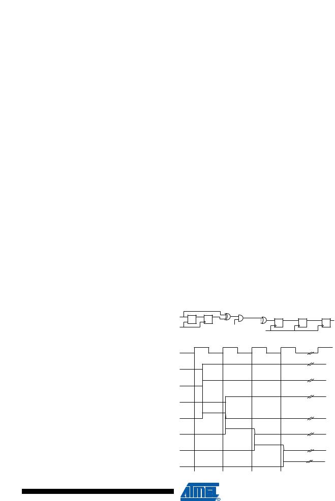
12.1Pin Change Interrupt Timing
An example of timing of a pin change interrupt is shown in Figure 12-1.
Figure 12-1. Timing of pin change interrupts
PCINT(0) |
pin_lat D Q |
pcint_in_(0) 0 |
pcint_syn |
pcint_setflag |
|
LE |
pin_sync |
|
PCIF |
|
x |
|
|
|
|
|
|
|
|
clk |
|
PCINT(0) in PCMSK(x) |
|
|
|
|
clk |
|
|
|
|
|
|
clk
PCINT(0)
pin_lat
pin_sync
pcint_in_(0)
pcint_syn
pcint_setflag
PCIF
67
2545M–AVR–09/07