

- •Features
- •1. Pin Configurations
- •1.1 Pin Descriptions
- •1.1.3 Port B (PB7:0) XTAL1/XTAL2/TOSC1/TOSC2
- •1.1.4 Port C (PC5:0)
- •1.1.5 PC6/RESET
- •1.1.6 Port D (PD7:0)
- •1.1.8 AREF
- •1.1.9 ADC7:6 (TQFP and QFN/MLF Package Only)
- •2. Overview
- •2.1 Block Diagram
- •2.2 Comparison Between ATmega48, ATmega88, and ATmega168
- •3. Resources
- •4. Data Retention
- •5. About Code Examples
- •6. AVR CPU Core
- •6.1 Overview
- •6.2 Architectural Overview
- •6.4 Status Register
- •6.5 General Purpose Register File
- •6.6 Stack Pointer
- •6.7 Instruction Execution Timing
- •6.8 Reset and Interrupt Handling
- •6.8.1 Interrupt Response Time
- •7. AVR Memories
- •7.1 Overview
- •7.3 SRAM Data Memory
- •7.3.1 Data Memory Access Times
- •7.4 EEPROM Data Memory
- •7.4.1 EEPROM Read/Write Access
- •7.4.2 Preventing EEPROM Corruption
- •7.5 I/O Memory
- •7.5.1 General Purpose I/O Registers
- •7.6 Register Description
- •8. System Clock and Clock Options
- •8.1 Clock Systems and their Distribution
- •8.2 Clock Sources
- •8.2.1 Default Clock Source
- •8.2.2 Clock Startup Sequence
- •8.3 Low Power Crystal Oscillator
- •8.4 Full Swing Crystal Oscillator
- •8.5 Low Frequency Crystal Oscillator
- •8.6 Calibrated Internal RC Oscillator
- •8.7 128 kHz Internal Oscillator
- •8.8 External Clock
- •8.9 Clock Output Buffer
- •8.10 Timer/Counter Oscillator
- •8.11 System Clock Prescaler
- •8.12 Register Description
- •9. Power Management and Sleep Modes
- •9.1 Sleep Modes
- •9.2 Idle Mode
- •9.3 ADC Noise Reduction Mode
- •9.4 Power-down Mode
- •9.5 Power-save Mode
- •9.6 Standby Mode
- •9.7 Power Reduction Register
- •9.8 Minimizing Power Consumption
- •9.8.1 Analog to Digital Converter
- •9.8.2 Analog Comparator
- •9.8.4 Internal Voltage Reference
- •9.8.5 Watchdog Timer
- •9.8.6 Port Pins
- •9.9 Register Description
- •10. System Control and Reset
- •10.1 Resetting the AVR
- •10.2 Reset Sources
- •10.3 Power-on Reset
- •10.4 External Reset
- •10.6 Watchdog System Reset
- •10.7 Internal Voltage Reference
- •10.8 Watchdog Timer
- •10.8.1 Features
- •10.9 Register Description
- •11. Interrupts
- •11.1 Overview
- •11.2 Interrupt Vectors in ATmega48
- •11.3 Interrupt Vectors in ATmega88
- •11.4 Interrupt Vectors in ATmega168
- •11.4.1 Moving Interrupts Between Application and Boot Space, ATmega88 and ATmega168
- •11.5 Register Description
- •12. External Interrupts
- •12.1 Pin Change Interrupt Timing
- •12.2 Register Description
- •13. I/O-Ports
- •13.1 Overview
- •13.2 Ports as General Digital I/O
- •13.2.1 Configuring the Pin
- •13.2.2 Toggling the Pin
- •13.2.3 Switching Between Input and Output
- •13.2.4 Reading the Pin Value
- •13.2.5 Digital Input Enable and Sleep Modes
- •13.2.6 Unconnected Pins
- •13.3 Alternate Port Functions
- •13.3.1 Alternate Functions of Port B
- •13.3.2 Alternate Functions of Port C
- •13.3.3 Alternate Functions of Port D
- •13.4 Register Description
- •14. 8-bit Timer/Counter0 with PWM
- •14.1 Features
- •14.2 Overview
- •14.2.1 Definitions
- •14.2.2 Registers
- •14.3 Timer/Counter Clock Sources
- •14.4 Counter Unit
- •14.5 Output Compare Unit
- •14.5.1 Force Output Compare
- •14.5.2 Compare Match Blocking by TCNT0 Write
- •14.5.3 Using the Output Compare Unit
- •14.6 Compare Match Output Unit
- •14.6.1 Compare Output Mode and Waveform Generation
- •14.7 Modes of Operation
- •14.7.1 Normal Mode
- •14.7.2 Clear Timer on Compare Match (CTC) Mode
- •14.7.3 Fast PWM Mode
- •14.7.4 Phase Correct PWM Mode
- •14.8 Timer/Counter Timing Diagrams
- •14.9 Register Description
- •15. 16-bit Timer/Counter1 with PWM
- •15.1 Features
- •15.2 Overview
- •15.2.1 Registers
- •15.2.2 Definitions
- •15.3.1 Reusing the Temporary High Byte Register
- •15.4 Timer/Counter Clock Sources
- •15.5 Counter Unit
- •15.6 Input Capture Unit
- •15.6.1 Input Capture Trigger Source
- •15.6.2 Noise Canceler
- •15.6.3 Using the Input Capture Unit
- •15.7 Output Compare Units
- •15.7.1 Force Output Compare
- •15.7.2 Compare Match Blocking by TCNT1 Write
- •15.7.3 Using the Output Compare Unit
- •15.8 Compare Match Output Unit
- •15.8.1 Compare Output Mode and Waveform Generation
- •15.9 Modes of Operation
- •15.9.1 Normal Mode
- •15.9.2 Clear Timer on Compare Match (CTC) Mode
- •15.9.3 Fast PWM Mode
- •15.9.4 Phase Correct PWM Mode
- •15.9.5 Phase and Frequency Correct PWM Mode
- •15.10 Timer/Counter Timing Diagrams
- •15.11 Register Description
- •16. Timer/Counter0 and Timer/Counter1 Prescalers
- •16.0.1 Internal Clock Source
- •16.0.2 Prescaler Reset
- •16.0.3 External Clock Source
- •16.1 Register Description
- •17. 8-bit Timer/Counter2 with PWM and Asynchronous Operation
- •17.1 Features
- •17.2 Overview
- •17.2.1 Registers
- •17.2.2 Definitions
- •17.3 Timer/Counter Clock Sources
- •17.4 Counter Unit
- •17.5 Output Compare Unit
- •17.5.1 Force Output Compare
- •17.5.2 Compare Match Blocking by TCNT2 Write
- •17.5.3 Using the Output Compare Unit
- •17.6 Compare Match Output Unit
- •17.6.1 Compare Output Mode and Waveform Generation
- •17.7 Modes of Operation
- •17.7.1 Normal Mode
- •17.7.2 Clear Timer on Compare Match (CTC) Mode
- •17.7.3 Fast PWM Mode
- •17.7.4 Phase Correct PWM Mode
- •17.8 Timer/Counter Timing Diagrams
- •17.9 Asynchronous Operation of Timer/Counter2
- •17.10 Timer/Counter Prescaler
- •17.11 Register Description
- •18.1 Features
- •18.2 Overview
- •18.3 SS Pin Functionality
- •18.3.1 Slave Mode
- •18.3.2 Master Mode
- •18.4 Data Modes
- •18.5 Register Description
- •19. USART0
- •19.1 Features
- •19.2 Overview
- •19.3 Clock Generation
- •19.3.2 Double Speed Operation (U2Xn)
- •19.3.3 External Clock
- •19.3.4 Synchronous Clock Operation
- •19.4 Frame Formats
- •19.4.1 Parity Bit Calculation
- •19.5 USART Initialization
- •19.6.1 Sending Frames with 5 to 8 Data Bit
- •19.6.2 Sending Frames with 9 Data Bit
- •19.6.3 Transmitter Flags and Interrupts
- •19.6.4 Parity Generator
- •19.6.5 Disabling the Transmitter
- •19.7.1 Receiving Frames with 5 to 8 Data Bits
- •19.7.2 Receiving Frames with 9 Data Bits
- •19.7.3 Receive Compete Flag and Interrupt
- •19.7.4 Receiver Error Flags
- •19.7.5 Parity Checker
- •19.7.6 Disabling the Receiver
- •19.7.7 Flushing the Receive Buffer
- •19.8 Asynchronous Data Reception
- •19.8.1 Asynchronous Clock Recovery
- •19.8.2 Asynchronous Data Recovery
- •19.8.3 Asynchronous Operational Range
- •19.9.1 Using MPCMn
- •19.10 Register Description
- •19.11 Examples of Baud Rate Setting
- •20. USART in SPI Mode
- •20.1 Features
- •20.2 Overview
- •20.3 Clock Generation
- •20.4 SPI Data Modes and Timing
- •20.5 Frame Formats
- •20.5.1 USART MSPIM Initialization
- •20.6 Data Transfer
- •20.6.1 Transmitter and Receiver Flags and Interrupts
- •20.6.2 Disabling the Transmitter or Receiver
- •20.7 AVR USART MSPIM vs. AVR SPI
- •20.8 Register Description
- •20.8.5 USART MSPIM Baud Rate Registers - UBRRnL and UBRRnH
- •21. 2-wire Serial Interface
- •21.1 Features
- •21.2.1 TWI Terminology
- •21.2.2 Electrical Interconnection
- •21.3 Data Transfer and Frame Format
- •21.3.1 Transferring Bits
- •21.3.2 START and STOP Conditions
- •21.3.3 Address Packet Format
- •21.3.4 Data Packet Format
- •21.3.5 Combining Address and Data Packets into a Transmission
- •21.5 Overview of the TWI Module
- •21.5.1 SCL and SDA Pins
- •21.5.2 Bit Rate Generator Unit
- •21.5.3 Bus Interface Unit
- •21.5.4 Address Match Unit
- •21.5.5 Control Unit
- •21.6 Using the TWI
- •21.7 Transmission Modes
- •21.7.1 Master Transmitter Mode
- •21.7.2 Master Receiver Mode
- •21.7.3 Slave Receiver Mode
- •21.7.4 Slave Transmitter Mode
- •21.7.5 Miscellaneous States
- •21.7.6 Combining Several TWI Modes
- •21.9 Register Description
- •22. Analog Comparator
- •22.1 Overview
- •22.2 Analog Comparator Multiplexed Input
- •22.3 Register Description
- •23. Analog-to-Digital Converter
- •23.1 Features
- •23.2 Overview
- •23.3 Starting a Conversion
- •23.4 Prescaling and Conversion Timing
- •23.5 Changing Channel or Reference Selection
- •23.5.1 ADC Input Channels
- •23.5.2 ADC Voltage Reference
- •23.6 ADC Noise Canceler
- •23.6.1 Analog Input Circuitry
- •23.6.2 Analog Noise Canceling Techniques
- •23.6.3 ADC Accuracy Definitions
- •23.7 ADC Conversion Result
- •23.8 Register Description
- •23.8.3.1 ADLAR = 0
- •23.8.3.2 ADLAR = 1
- •24. debugWIRE On-chip Debug System
- •24.1 Features
- •24.2 Overview
- •24.3 Physical Interface
- •24.4 Software Break Points
- •24.5 Limitations of debugWIRE
- •24.6 Register Description
- •25. Self-Programming the Flash, ATmega48
- •25.1 Overview
- •25.1.1 Performing Page Erase by SPM
- •25.1.2 Filling the Temporary Buffer (Page Loading)
- •25.1.3 Performing a Page Write
- •25.2.1 EEPROM Write Prevents Writing to SPMCSR
- •25.2.2 Reading the Fuse and Lock Bits from Software
- •25.2.3 Preventing Flash Corruption
- •25.2.4 Programming Time for Flash when Using SPM
- •25.2.5 Simple Assembly Code Example for a Boot Loader
- •25.3 Register Description
- •26.1 Features
- •26.2 Overview
- •26.3 Application and Boot Loader Flash Sections
- •26.3.1 Application Section
- •26.5 Boot Loader Lock Bits
- •26.6 Entering the Boot Loader Program
- •26.8.1 Performing Page Erase by SPM
- •26.8.2 Filling the Temporary Buffer (Page Loading)
- •26.8.3 Performing a Page Write
- •26.8.4 Using the SPM Interrupt
- •26.8.5 Consideration While Updating BLS
- •26.8.7 Setting the Boot Loader Lock Bits by SPM
- •26.8.8 EEPROM Write Prevents Writing to SPMCSR
- •26.8.9 Reading the Fuse and Lock Bits from Software
- •26.8.10 Preventing Flash Corruption
- •26.8.11 Programming Time for Flash when Using SPM
- •26.8.12 Simple Assembly Code Example for a Boot Loader
- •26.8.13 ATmega88 Boot Loader Parameters
- •26.8.14 ATmega168 Boot Loader Parameters
- •26.9 Register Description
- •27. Memory Programming
- •27.1 Program And Data Memory Lock Bits
- •27.2 Fuse Bits
- •27.2.1 Latching of Fuses
- •27.3 Signature Bytes
- •27.4 Calibration Byte
- •27.5 Page Size
- •27.6 Parallel Programming Parameters, Pin Mapping, and Commands
- •27.6.1 Signal Names
- •27.7 Parallel Programming
- •27.7.1 Enter Programming Mode
- •27.7.2 Considerations for Efficient Programming
- •27.7.3 Chip Erase
- •27.7.4 Programming the Flash
- •27.7.5 Programming the EEPROM
- •27.7.6 Reading the Flash
- •27.7.7 Reading the EEPROM
- •27.7.8 Programming the Fuse Low Bits
- •27.7.9 Programming the Fuse High Bits
- •27.7.10 Programming the Extended Fuse Bits
- •27.7.11 Programming the Lock Bits
- •27.7.12 Reading the Fuse and Lock Bits
- •27.7.13 Reading the Signature Bytes
- •27.7.14 Reading the Calibration Byte
- •27.7.15 Parallel Programming Characteristics
- •27.8 Serial Downloading
- •27.8.1 Serial Programming Pin Mapping
- •27.8.2 Serial Programming Algorithm
- •27.8.3 Serial Programming Instruction set
- •27.8.4 SPI Serial Programming Characteristics
- •28. Electrical Characteristics
- •28.1 Absolute Maximum Ratings*
- •28.2 DC Characteristics
- •28.3 Speed Grades
- •28.4 Clock Characteristics
- •28.4.1 Calibrated Internal RC Oscillator Accuracy
- •28.4.2 External Clock Drive Waveforms
- •28.4.3 External Clock Drive
- •28.5 System and Reset Characteristics
- •28.7 SPI Timing Characteristics
- •28.8 ADC Characteristics
- •28.9 Parallel Programming Characteristics
- •29. Typical Characteristics
- •29.1 Active Supply Current
- •29.2 Idle Supply Current
- •29.3 Supply Current of I/O modules
- •29.3.0.1 Example 1
- •29.3.0.2 Example 2
- •29.3.0.3 Example 3
- •29.6 Standby Supply Current
- •29.8 Pin Driver Strength
- •29.9 Pin Thresholds and Hysteresis
- •29.10 BOD Thresholds and Analog Comparator Offset
- •29.11 Internal Oscillator Speed
- •29.12 Current Consumption of Peripheral Units
- •29.13 Current Consumption in Reset and Reset Pulse width
- •30. Register Summary
- •31. Instruction Set Summary
- •32. Ordering Information
- •32.1 ATmega48
- •32.2 ATmega88
- •32.3 ATmega168
- •33. Packaging Information
- •34. Errata
- •34.1 Errata ATmega48
- •34.2 Errata ATmega88
- •34.3 Errata ATmega168
- •35. Datasheet Revision History

 ATmega48/88/168
27.7.14Reading the Calibration Byte
The algorithm for reading the Calibration byte is as follows (refer to “Programming the Flash” on page 293 for details on Command and Address loading):
1.A: Load Command “0000 1000”.
2.B: Load Address Low Byte, 0x00.
3.Set OE to “0”, and BS1 to “1”. The Calibration byte can now be read at DATA.
4.Set OE to “1”.
27.7.15Parallel Programming Characteristics
For characteristics of the parallel programming, see “Parallel Programming Characteristics” on page 313.
27.8Serial Downloading
Both the Flash and EEPROM memory arrays can be programmed using the serial SPI bus while RESET is pulled to GND. The serial interface consists of pins SCK, MOSI (input) and MISO (output). After RESET is set low, the Programming Enable instruction needs to be executed first before program/erase operations can be executed. NOTE, in Table 27-15 on page 300, the pin mapping for SPI programming is listed. Not all parts use the SPI pins dedicated for the internal SPI interface.
Figure 27-7. Serial Programming and Verify(1)
+1.8 - 5.5V
VCC
+1.8 - 5.5V(2)
MOSI
AVCC
MISO 
SCK
 XTAL1
XTAL1
RESET
GND
Notes: 1. If the device is clocked by the internal Oscillator, it is no need to connect a clock source to the XTAL1 pin.
2. VCC - 0.3V < AVCC < VCC + 0.3V, however, AVCC should always be within 1.8 - 5.5V
When programming the EEPROM, an auto-erase cycle is built into the self-timed programming operation (in the Serial mode ONLY) and there is no need to first execute the Chip Erase instruction. The Chip Erase operation turns the content of every memory location in both the Program and EEPROM arrays into 0xFF.
Depending on CKSEL Fuses, a valid clock must be present. The minimum low and high periods for the serial clock (SCK) input are defined as follows:
Low: > 2 CPU clock cycles for fck < 12 MHz, 3 CPU clock cycles for fck >= 12 MHz
High: > 2 CPU clock cycles for fck < 12 MHz, 3 CPU clock cycles for fck >= 12 MHz
299
2545M–AVR–09/07

27.8.1Serial Programming Pin Mapping
Table 27-15. Pin Mapping Serial Programming
Symbol |
Pins |
I/O |
Description |
|
|
|
|
MOSI |
PB3 |
I |
Serial Data in |
|
|
|
|
MISO |
PB4 |
O |
Serial Data out |
|
|
|
|
SCK |
PB5 |
I |
Serial Clock |
|
|
|
|
27.8.2Serial Programming Algorithm
When writing serial data to the ATmega48/88/168, data is clocked on the rising edge of SCK.
When reading data from the ATmega48/88/168, data is clocked on the falling edge of SCK. See
Figure 27-9 for timing details.
To program and verify the ATmega48/88/168 in the serial programming mode, the following sequence is recommended (See Serial Programming Instruction set in Table 27-17 on page 301):
1.Power-up sequence:
Apply power between VCC and GND while RESET and SCK are set to “0”. In some systems, the programmer can not guarantee that SCK is held low during power-up. In this case, RESET must be given a positive pulse of at least two CPU clock cycles duration after SCK has been set to “0”.
2.Wait for at least 20 ms and enable serial programming by sending the Programming Enable serial instruction to pin MOSI.
3.The serial programming instructions will not work if the communication is out of synchronization. When in sync. the second byte (0x53), will echo back when issuing the third byte of the Programming Enable instruction. Whether the echo is correct or not, all four bytes of the instruction must be transmitted. If the 0x53 did not echo back, give RESET a positive pulse and issue a new Programming Enable command.
4.The Flash is programmed one page at a time. The memory page is loaded one byte at a time by supplying the 6 LSB of the address and data together with the Load Program Memory Page instruction. To ensure correct loading of the page, the data low byte must be loaded before data high byte is applied for a given address. The Program Memory Page is stored by loading the Write Program Memory Page instruction with the 7 MSB of
the address. If polling (RDY/BSY) is not used, the user must wait at least tWD_FLASH before issuing the next page (See Table 27-16). Accessing the serial programming interface before the Flash write operation completes can result in incorrect programming.
5.A: The EEPROM array is programmed one byte at a time by supplying the address and data together with the appropriate Write instruction. An EEPROM memory location is first automatically erased before new data is written. If polling (RDY/BSY) is not used, the
user must wait at least tWD_EEPROM before issuing the next byte (See Table 27-16). In a chip erased device, no 0xFFs in the data file(s) need to be programmed.
B: The EEPROM array is programmed one page at a time. The Memory page is loaded one byte at a time by supplying the 6 LSB of the address and data together with the Load EEPROM Memory Page instruction. The EEPROM Memory Page is stored by loading the Write EEPROM Memory Page Instruction with the 7 MSB of the address. When using EEPROM page access only byte locations loaded with the Load EEPROM Memory Page instruction is altered. The remaining locations remain unchanged. If polling (RDY/BSY) is
not used, the used must wait at least tWD_EEPROM before issuing the next byte (See Table 27-16). In a chip erased device, no 0xFF in the data file(s) need to be programmed.
300 ATmega48/88/168 
2545M–AVR–09/07
ATmega48/88/168
6.Any memory location can be verified by using the Read instruction which returns the content at the selected address at serial output MISO.
7.At the end of the programming session, RESET can be set high to commence normal operation.
8.Power-off sequence (if needed): Set RESET to “1”.
Turn VCC power off.
Table 27-16. Typical Wait Delay Before Writing the Next Flash or EEPROM Location
Symbol |
Minimum Wait Delay |
|
|
tWD_FLASH |
4.5 ms |
tWD_EEPROM |
3.6 ms |
tWD_ERASE |
9.0 ms |
27.8.3Serial Programming Instruction set
Table 27-17 on page 301 and Figure 27-8 on page 302 describes the Instruction set.
Table 27-17. Serial Programming Instruction Set (Hexadecimal values)
|
|
|
|
Instruction Format |
|
|
|
|
|
|
|
||
Instruction/Operation |
Byte 1 |
Byte 2 |
Byte 3 |
Byte4 |
||
|
|
|
|
|
||
Programming Enable |
$AC |
$53 |
$00 |
$00 |
||
|
|
|
|
|
||
Chip Erase (Program Memory/EEPROM) |
$AC |
$80 |
$00 |
$00 |
||
|
|
|
|
|
|
|
|
|
|
$F0 |
$00 |
$00 |
data byte out |
Poll RDY/BSY |
|
|||||
|
|
|
|
|
||
Load Instructions |
|
|
|
|
||
|
|
|
|
|
||
Load Extended Address byte(1) |
$4D |
$00 |
Extended adr |
$00 |
||
Load Program Memory Page, High byte |
$48 |
$00 |
adr LSB |
high data byte in |
||
|
|
|
|
|
||
Load Program Memory Page, Low byte |
$40 |
$00 |
adr LSB |
low data byte in |
||
|
|
|
|
|
||
Load EEPROM Memory Page (page access) |
$C1 |
$00 |
0000 000aa |
data byte in |
||
|
|
|
|
|
||
Read Instructions |
|
|
|
|
||
|
|
|
|
|
||
Read Program Memory, High byte |
$28 |
adr MSB |
adr LSB |
high data byte out |
||
|
|
|
|
|
||
Read Program Memory, Low byte |
$20 |
adr MSB |
adr LSB |
low data byte out |
||
|
|
|
|
|
||
Read EEPROM Memory |
$A0 |
0000 00aa |
aaaa aaaa |
data byte out |
||
|
|
|
|
|
||
Read Lock bits |
$58 |
$00 |
$00 |
data byte out |
||
|
|
|
|
|
||
Read Signature Byte |
$30 |
$00 |
0000 000aa |
data byte out |
||
|
|
|
|
|
||
Read Fuse bits |
$50 |
$00 |
$00 |
data byte out |
||
|
|
|
|
|
||
Read Fuse High bits |
$58 |
$08 |
$00 |
data byte out |
||
|
|
|
|
|
||
Read Extended Fuse Bits |
$50 |
$08 |
$00 |
data byte out |
||
|
|
|
|
|
||
Read Calibration Byte |
$38 |
$00 |
$00 |
data byte out |
||
|
|
|
|
|
||
Write Instructions(6) |
|
|
|
|
||
Write Program Memory Page |
$4C |
adr MSB |
adr LSB |
$00 |
||
|
|
|
|
|
||
Write EEPROM Memory |
$C0 |
0000 00aa |
aaaa aaaa |
data byte in |
||
|
|
|
|
|
|
|
301
2545M–AVR–09/07
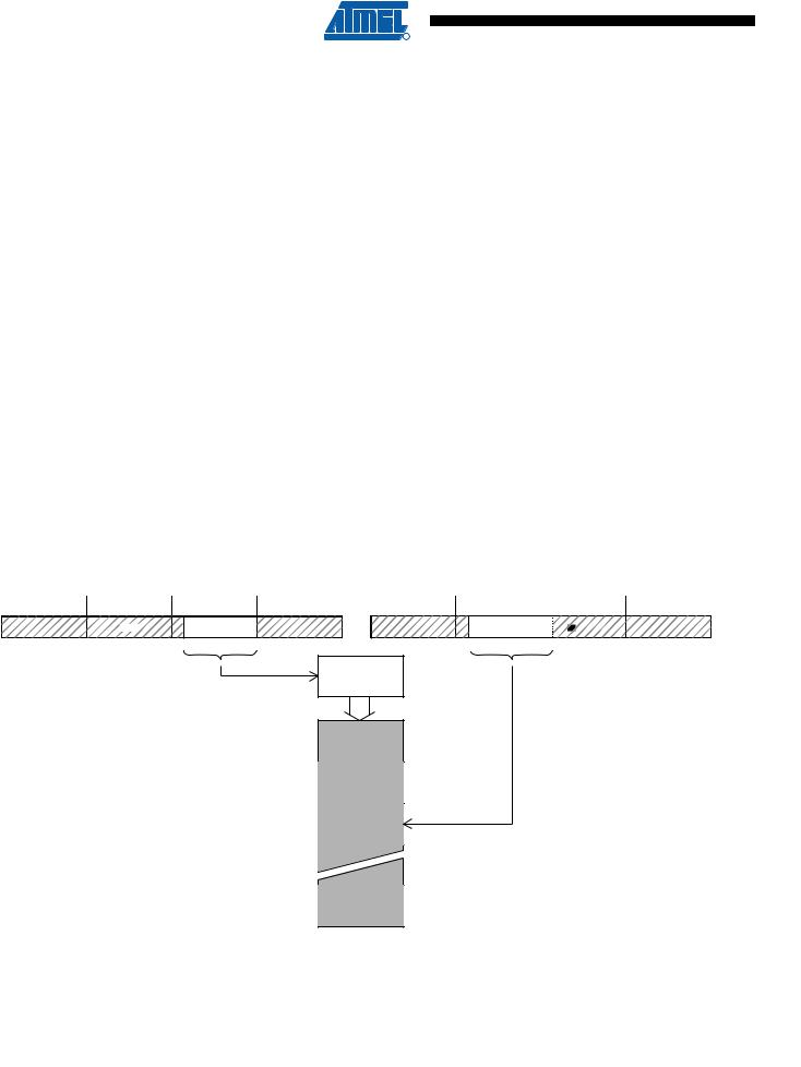
Table 27-17. Serial Programming Instruction Set (Hexadecimal values) (Continued)
|
|
Instruction Format |
|
|
|
|
|
|
|
Instruction/Operation |
Byte 1 |
Byte 2 |
Byte 3 |
Byte4 |
|
|
|
|
|
Write EEPROM Memory Page (page access) |
$C2 |
0000 00aa |
aaaa aa00 |
$00 |
|
|
|
|
|
Write Lock bits |
$AC |
$E0 |
$00 |
data byte in |
|
|
|
|
|
Write Fuse bits |
$AC |
$A0 |
$00 |
data byte in |
|
|
|
|
|
Write Fuse High bits |
$AC |
$A8 |
$00 |
data byte in |
|
|
|
|
|
Write Extended Fuse Bits |
$AC |
$A4 |
$00 |
data byte in |
|
|
|
|
|
Notes: 1. Not all instructions are applicable for all parts.
2.a = address.
3.Bits are programmed ‘0’, unprogrammed ‘1’.
4.To ensure future compatibility, unused Fuses and Lock bits should be unprogrammed (‘1’) .
5.Refer to the correspondig section for Fuse and Lock bits, Calibration and Signature bytes and Page size.
6.Instructions accessing program memory use a word address. This word may be random within the page range.
7.See htt://www.atmel.com/avr for Application Notes regarding programming and programmers.
If the LSB in RDY/BSY data byte out is ‘1’, a programming operation is still pending. Wait until this bit returns ‘0’ before the next instruction is carried out.
Within the same page, the low data byte must be loaded prior to the high data byte.
After data is loaded to the page buffer, program the EEPROM page, see Figure 27-8 on page 302.
Figure 27-8. Serial Programming Instruction example
Serial Programming Instruction
Load Program Memory Page (High/Low Byte)/ |
Write Program Memory Page/ |
Load EEPROM Memory Page (page access) |
Write EEPROM Memory Page |
Byte 1 |
Byte 2 |
Byte 3 |
Byte 4 |
Byte 1 |
Byte 2 |
Byte 3 |
Byte 4 |
|||||
|
|
|
|
Adr LSB |
|
|
Adr MSB |
|
|
|
|
|
|
|
|
|
|
|
|
|
|
|
|
||
|
|
Adr |
MSB |
|
|
Adr |
LSBB |
|
||||
|
|
|
|
|
Bit 15 |
B |
|
|
|
|
0 |
|
Bit 15 |
B |
|
0 |
|
|
|
|
|||||
Page Buffer
Page Offset
Page 0
Page 1
Page 2
Page Number
Page N-1
Program Memory/
EEPROM Memory
302 ATmega48/88/168 
2545M–AVR–09/07