

- •Features
- •Disclaimer
- •Overview
- •Block Diagram
- •Pin Descriptions
- •Port A (PA7..PA0)
- •Port B (PB7..PB0)
- •Port C (PC7..PC0)
- •Port D (PD7..PD0)
- •RESET
- •XTAL1
- •XTAL2
- •AVCC
- •AREF
- •Resources
- •Data Retention
- •AVR CPU Core
- •Introduction
- •Status Register
- •Stack Pointer
- •I/O Memory
- •Clock Systems and their Distribution
- •Clock Sources
- •Crystal Oscillator
- •External Clock
- •Idle Mode
- •Power-down Mode
- •Power-save Mode
- •Standby Mode
- •Analog Comparator
- •Brown-out Detector
- •Watchdog Timer
- •Port Pins
- •Resetting the AVR
- •Reset Sources
- •Power-on Reset
- •External Reset
- •Watchdog Reset
- •Watchdog Timer
- •Interrupts
- •I/O Ports
- •Introduction
- •Configuring the Pin
- •Reading the Pin Value
- •Unconnected pins
- •Alternate Port Functions
- •Register Description for I/O Ports
- •8-bit Timer/Counter0 with PWM
- •Overview
- •Registers
- •Definitions
- •Counter Unit
- •Normal Mode
- •Fast PWM Mode
- •8-bit Timer/Counter Register Description
- •Timer/Counter0 and Timer/Counter1 Prescalers
- •Internal Clock Source
- •Prescaler Reset
- •External Clock Source
- •16-bit Timer/Counter1
- •Overview
- •Registers
- •Definitions
- •Compatibility
- •Counter Unit
- •Input Capture Unit
- •Noise Canceler
- •Force Output Compare
- •Normal Mode
- •Fast PWM Mode
- •16-bit Timer/Counter Register Description
- •8-bit Timer/Counter2 with PWM and Asynchronous Operation
- •Overview
- •Registers
- •Definitions
- •Counter Unit
- •Normal Mode
- •Fast PWM Mode
- •8-bit Timer/Counter Register Description
- •Slave Mode
- •Master Mode
- •Data Modes
- •USART
- •Overview
- •Clock Generation
- •External Clock
- •Frame Formats
- •Parity Bit Calculation
- •Parity Generator
- •Receiver Error Flags
- •Parity Checker
- •Disabling the Receiver
- •Using MPCM
- •Write Access
- •Read Access
- •Features
- •TWI Terminology
- •Transferring Bits
- •Address Packet Format
- •Data Packet Format
- •Overview of the TWI Module
- •SCL and SDA Pins
- •Bus Interface Unit
- •Address Match Unit
- •Control Unit
- •Using the TWI
- •Master Receiver Mode
- •Slave Receiver Mode
- •Miscellaneous States
- •Analog Comparator Multiplexed Input
- •Analog to Digital Converter
- •Features
- •Operation
- •Changing Channel or Reference Selection
- •ADC Input Channels
- •Analog Input Circuitry
- •Features
- •Overview
- •TAP Controller
- •PRIVATE0; $8
- •PRIVATE1; $9
- •PRIVATE2; $A
- •PRIVATE3; $B
- •Bibliography
- •IEEE 1149.1 (JTAG) Boundary-scan
- •Features
- •System Overview
- •Data Registers
- •Bypass Register
- •Reset Register
- •EXTEST; $0
- •IDCODE; $1
- •AVR_RESET; $C
- •BYPASS; $F
- •Scanning the ADC
- •ATmega16 Boundary-scan Order
- •Features
- •Application Section
- •Read-While-Write and no Read- While-Write Flash Sections
- •Prevent Reading the RWW Section during Self-Programming
- •Simple Assembly Code Example for a Boot Loader
- •Fuse Bits
- •Latching of Fuses
- •Signature Bytes
- •Calibration Byte
- •Page Size
- •Signal Names
- •Chip Erase
- •Reading the Flash
- •Reading the EEPROM
- •Data Polling Flash
- •Data Polling EEPROM
- •AVR_RESET ($C)
- •PROG_ENABLE ($4)
- •Data Registers
- •Reset Register
- •Programming Enable Register
- •Programming Command Register
- •Virtual Flash Page Read Register
- •Performing Chip Erase
- •Reading the Flash
- •Reading the EEPROM
- •Electrical Characteristics
- •Absolute Maximum Ratings*
- •DC Characteristics
- •External Clock Drive Waveforms
- •External Clock Drive
- •Two-wire Serial Interface Characteristics
- •ADC Characteristics
- •Idle Supply Current
- •Pin Pullup
- •Pin Driver Strength
- •Register Summary
- •Instruction Set Summary
- •Ordering Information
- •Packaging Information
- •Errata

 ATmega16(L)
Parallel
Programming
Enter Programming |
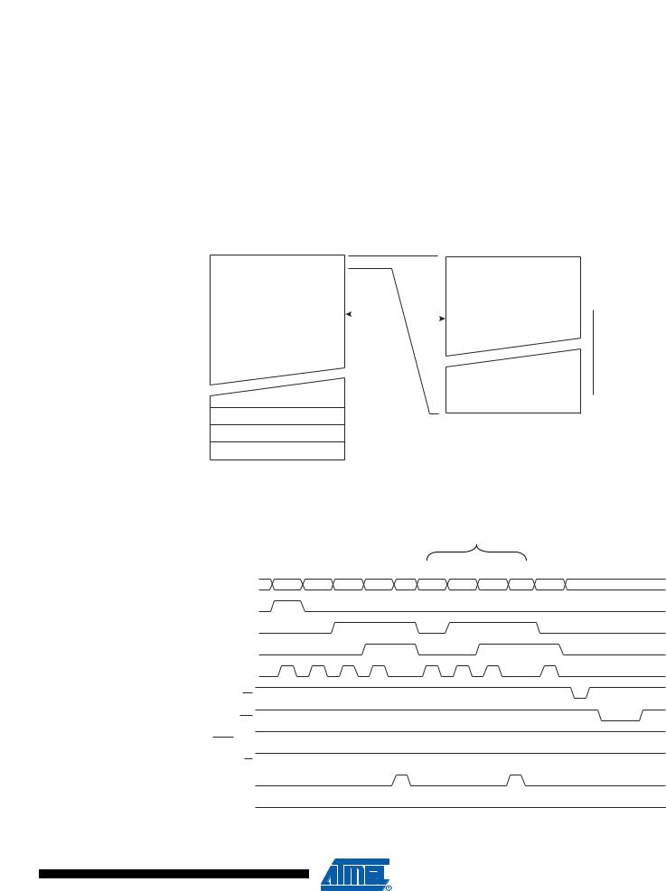
The following algorithm puts the device in Parallel Programming mode: |
|||||||
Mode |
1. |
Apply 4.5 - 5.5V between VCC and GND, and wait at least 100 µs. |
||||||
|
||||||||
|
2. |
Set |
|
to “0” and toggle XTAL1 at least 6 times |
||||
|
RESET |
|||||||
|
3. |
Set the Prog_enable pins listed in Table 110 on page 263 to “0000” and wait at least 100 |
||||||
|
|
ns. |
||||||
|
4. |
Apply 11.5 - 12.5V to |
|
|
Any activity on Prog_enable pins within 100 ns after +12V |
|||
|
RESET. |
|||||||
|
|
has been applied to |
RESET, |
will cause the device to fail entering Programming mode. |
||||
Note, if External Crystal or External RC configuration is selected, it may not be possible to apply qualified XTAL1 pulses. In such cases, the following algorithm should be followed:
1.Set Prog_enable pins listed in Table 110 on page 263 to “0000”.
2.Apply 4.5 - 5.5V between VCC and GND simultaneously as 11.5 - 12.5V is applied to RESET.
3.Wait 100 µs.
4.Re-program the fuses to ensure that External Clock is selected as clock source (CKSEL3:0 = 0b0000) If Lock bits are programmed, a Chip Erase command must be executed before changing the fuses.
5.Exit Programming mode by power the device down or by bringing RESET pin to 0b0.
6.Entering Programming mode with the original algorithm, as described above.
Considerations for The loaded command and address are retained in the device during programming. For efficient Efficient Programming programming, the following should be considered.
•The command needs only be loaded once when writing or reading multiple memory locations.
•Skip writing the data value $FF, that is the contents of the entire EEPROM (unless the EESAVE Fuse is programmed) and Flash after a Chip Erase.
•Address High byte needs only be loaded before programming or reading a new 256 word window in Flash or 256 byte EEPROM. This consideration also applies to Signature bytes reading.
Chip Erase |
The Chip Erase will erase the Flash and EEPROM(1) memories plus Lock bits. The Lock bits are |
|||||||||||
|
not reset until the program memory has been completely erased. The Fuse bits are not |
|||||||||||
|
changed. A Chip Erase must be performed before the Flash and/or the EEPROM are |
|||||||||||
|
reprogrammed. |
|||||||||||
|
Note: 1. The EEPRPOM memory is preserved during chip erase if the EESAVE Fuse is programmed. |
|||||||||||
|
Load Command “Chip Erase” |
|||||||||||
|
1. |
Set XA1, XA0 to “10”. This enables command loading. |
||||||||||
|
2. |
Set BS1 to “0”. |
||||||||||
|
3. |
Set DATA to “1000 0000”. This is the command for Chip Erase. |
||||||||||
|
4. |
Give XTAL1 a positive pulse. This loads the command. |
||||||||||
|
5. |
Give |
|
|
|
|
|
goes low. |
||||
|
WR |
a negative pulse. This starts the Chip Erase. RDY/BSY |
||||||||||
|
6. |
|
|
goes high before loading a new command. |
||||||||
|
Wait until RDY/BSY |
|||||||||||
Programming the |
The Flash is organized in pages, see Table 107 on page 262. When programming the Flash, the |
|||||||||||
Flash |
program data is latched into a page buffer. This allows one page of program data to be pro- |
|||||||||||
|
|
|
|
|
|
|
|
|
|
|
|
|
|
|
|
|
|
|
|
|
|
|
265 |
||
|
|
|
|
|
|
|
|
|
|
|||
|
|
|
|
|
|
|
|
|
|
|||
2466P–AVR–08/07

grammed simultaneously. The following procedure describes how to program the entire Flash memory:
A. Load Command “Write Flash”
1.Set XA1, XA0 to “10”. This enables command loading.
2.Set BS1 to “0”.
3.Set DATA to “0001 0000”. This is the command for Write Flash.
4.Give XTAL1 a positive pulse. This loads the command.
B. Load Address Low byte
1.Set XA1, XA0 to “00”. This enables address loading.
2.Set BS1 to “0”. This selects low address.
3.Set DATA = Address Low byte ($00 - $FF).
4.Give XTAL1 a positive pulse. This loads the address Low byte.
C. Load Data Low Byte
1.Set XA1, XA0 to “01”. This enables data loading.
2.Set DATA = Data Low byte ($00 - $FF).
3.Give XTAL1 a positive pulse. This loads the data byte.
D. Load Data High Byte
1.Set BS1 to “1”. This selects high data byte.
2.Set XA1, XA0 to “01”. This enables data loading.
3.Set DATA = Data High byte ($00 - $FF).
4.Give XTAL1 a positive pulse. This loads the data byte.
E. Latch Data
1.Set BS1 to “1”. This selects high data byte.
2.Give PAGEL a positive pulse. This latches the data bytes. (See Figure 129 for signal waveforms)
F. Repeat B through E until the entire buffer is filled or until all data within the page is loaded.
While the lower bits in the address are mapped to words within the page, the higher bits address the pages within the FLASH. This is illustrated in Figure 128 on page 267. Note that if less than 8 bits are required to address words in the page (pagesize < 256), the most significant bit(s) in the address Low byte are used to address the page when performing a page write.
G. Load Address High byte
1.Set XA1, XA0 to “00”. This enables address loading.
2.Set BS1 to “1”. This selects high address.
3.Set DATA = Address High byte ($00 - $FF).
4.Give XTAL1 a positive pulse. This loads the address High byte.
H. Program Page
1.Set BS1 = “0”
2.Give WR a negative pulse. This starts programming of the entire page of data. RDY/BSY goes low.
3.Wait until RDY/BSY goes high. (See Figure 129 for signal waveforms)
I. Repeat B through H until the entire Flash is programmed or until all data has been programmed.
266 ATmega16(L) 
2466P–AVR–08/07
 ATmega16(L)
J. End Page Programming
1.1. Set XA1, XA0 to “10”. This enables command loading.
2.Set DATA to “0000 0000”. This is the command for No Operation.
3.Give XTAL1 a positive pulse. This loads the command, and the internal write signals are reset.
Figure 128. Addressing the Flash which is Organized in Pages
|
PROGRAM |
PCMSB |
|
|
|
|
PAGEMSB |
|
|||||||
|
|
PCPAGE |
PCWORD |
|
|
|
|
||||||||
|
COUNTER |
|
|
|
|
|
|||||||||
|
|
|
|
|
|
|
|
|
|
|
|
|
|
||
|
PAGE ADDRESS |
|
|
WORD ADDRESS |
|
||||||||||
|
WITHIN THE FLASH |
|
|
WITHIN A PAGE |
|
||||||||||
PROGRAM MEMORY |
|
|
|
|
|
|
|
|
|
PAGE |
PCWORD[PAGEMSB:0]: |
||||
|
|
|
|
|
|
|
|
|
|
|
|
|
|
|
|
|
PAGE |
|
|
|
|
|
|
|
|
INSTRUCTION WORD |
00 |
||||
|
|
|
|
|
|
|
|
|
|
|
|
||||
|
|
|
|
|
|
|
|
|
|
|
|
|
|
|
01 |
|
|
|
|
|
|
|
|
|
|
|
|
|
|
|
|
|
|
|
|
|
|
|
|
|
|
|
|
|
|
|
02 |
|
|
|
|
|
|
|
|
|
|
|
|
|
|
|
|
|
|
|
|
|
|
|
|
|
|
|
|
|
|
|
|
|
|
|
|
|
|
|
|
|
|
|
|
|
|
|
|
|
|
|
|
|
|
|
|
|
|
|
|
|
|
|
|
|
|
|
|
|
|
|
|
|
|
|
|
|
|
|
|
|
|
|
|
|
|
|
|
|
|
|
|
|
|
|
|
|
|
|
|
|
|
|
|
|
|
|
|
|
|
|
|
|
|
|
|
|
|
|
|
|
|
|
|
|
|
|
|
|
|
|
|
|
|
|
|
|
|
|
|
|
|
|
|
|
|
|
|
|
|
|
|
|
|
|
|
|
|
|
|
|
|
|
|
|
|
|
|
|
|
|
|
|
|
|
|
|
|
|
|
|
|
|
|
|
|
|
|
|
|
|
|
|
|
|
|
|
|
|
|
|
|
|
|
|
|
|
|
|
|
|
|
|
|
|
|
|
|
|
|
|
|
|
|
PAGEEND
Note: 1. PCPAGE and PCWORD are listed in Table 107 on page 262.
Figure 129. Programming the Flash Waveforms(1)
|
|
|
|
|
|
|
|
|
|
F |
|
|
|
|
|
|
A |
B |
C |
D |
E |
B |
C |
D |
E |
G |
H |
|
DATA |
$10 |
ADDR. LOW |
DATA LOW |
DATA HIGH |
XX |
ADDR. LOW |
DATA LOW |
DATA HIGH |
XX |
ADDR. HIGH |
XX |
|
|
|
|
|
|
|
|
|
|
|
|
|
||
|
|
XA1 |
|
|
|
|
|
|
|
|
|
|
|
|
|
XA0 |
|
|
|
|
|
|
|
|
|
|
|
|
|
BS1 |
|
|
|
|
|
|
|
|
|
|
|
|
XTAL1 |
|
|
|
|
|
|
|
|
|
|
|
|
|
|
WR |
|
|
|
|
|
|
|
|
|
|
|
|
RDY/BSY |
|
|
|
|
|
|
|
|
|
|
|
|
|
RESET |
+12V |
|
|
|
|
|
|
|
|
|
|
|
|
|
OE |
|
|
|
|
|
|
|
|
|
|
|
|
PAGEL |
|
|
|
|
|
|
|
|
|
|
|
|
|
|
BS2 |
|
|
|
|
|
|
|
|
|
|
|
Note: |
1. |
“XX” is don’t care. The letters refer to the programming description above. |
|||||||||||
267
2466P–AVR–08/07
Programming the The EEPROM is organized in pages, see Table 108 on page 262. When programming the EEPROM EEPROM, the program data is latched into a page buffer. This allows one page of data to be programmed simultaneously. The programming algorithm for the EEPROM data memory is as follows (refer to “Programming the Flash” on page 265 for details on Command, Address and
Data loading):
1.A: Load Command “0001 0001”.
2.G: Load Address High Byte ($00 - $FF)
3.B: Load Address Low Byte ($00 - $FF)
4.C: Load Data ($00 - $FF)
5.E: Latch data (give PAGEL a positive pulse)
K:Repeat 3 through 5 until the entire buffer is filled
L:Program EEPROM page
1.Set BS1 to “0”.
2.Give WR a negative pulse. This starts programming of the EEPROM page. RDY/BSY goes low.
3.Wait until to RDY/BSY goes high before programming the next page. (See Figure 130 for signal waveforms)
Figure 130. Programming the EEPROM Waveforms
|
|
|
|
|
|
|
K |
|
|
|
A |
G |
B |
C |
E |
B |
C |
E |
L |
DATA |
0x11 |
ADDR. HIGH ADDR. LOW |
DATA |
XX |
ADDR. LOW |
DATA |
XX |
|
|
|
|
|
|
|
|
|
|
|
|
XA1
XA0
BS1
XTAL1
WR
RDY/BSY
RESET +12V
OE
PAGEL
BS2
Reading the Flash The algorithm for reading the Flash memory is as follows (refer to “Programming the Flash” on page 265 for details on Command and Address loading):
1.A: Load Command “0000 0010”.
2.G: Load Address High Byte ($00 - $FF)
3.B: Load Address Low Byte ($00 - $FF)
4.Set OE to “0”, and BS1 to “0”. The Flash word Low byte can now be read at DATA.
5.Set BS1 to “1”. The Flash word High byte can now be read at DATA.
268 ATmega16(L) 
2466P–AVR–08/07