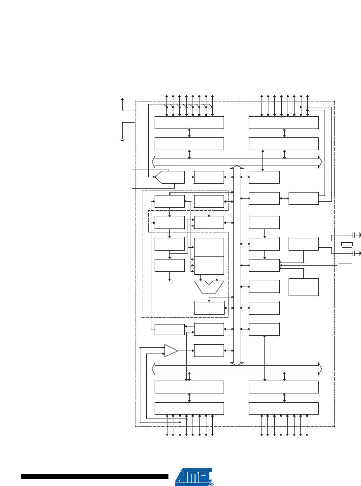
 
        
        - •Features
- •Disclaimer
- •Overview
- •Block Diagram
- •Pin Descriptions
- •Port A (PA7..PA0)
- •Port B (PB7..PB0)
- •Port C (PC7..PC0)
- •Port D (PD7..PD0)
- •RESET
- •XTAL1
- •XTAL2
- •AVCC
- •AREF
- •Resources
- •Data Retention
- •AVR CPU Core
- •Introduction
- •Status Register
- •Stack Pointer
- •I/O Memory
- •Clock Systems and their Distribution
- •Clock Sources
- •Crystal Oscillator
- •External Clock
- •Idle Mode
- •Power-down Mode
- •Power-save Mode
- •Standby Mode
- •Analog Comparator
- •Brown-out Detector
- •Watchdog Timer
- •Port Pins
- •Resetting the AVR
- •Reset Sources
- •Power-on Reset
- •External Reset
- •Watchdog Reset
- •Watchdog Timer
- •Interrupts
- •I/O Ports
- •Introduction
- •Configuring the Pin
- •Reading the Pin Value
- •Unconnected pins
- •Alternate Port Functions
- •Register Description for I/O Ports
- •8-bit Timer/Counter0 with PWM
- •Overview
- •Registers
- •Definitions
- •Counter Unit
- •Normal Mode
- •Fast PWM Mode
- •8-bit Timer/Counter Register Description
- •Timer/Counter0 and Timer/Counter1 Prescalers
- •Internal Clock Source
- •Prescaler Reset
- •External Clock Source
- •16-bit Timer/Counter1
- •Overview
- •Registers
- •Definitions
- •Compatibility
- •Counter Unit
- •Input Capture Unit
- •Noise Canceler
- •Force Output Compare
- •Normal Mode
- •Fast PWM Mode
- •16-bit Timer/Counter Register Description
- •8-bit Timer/Counter2 with PWM and Asynchronous Operation
- •Overview
- •Registers
- •Definitions
- •Counter Unit
- •Normal Mode
- •Fast PWM Mode
- •8-bit Timer/Counter Register Description
- •Slave Mode
- •Master Mode
- •Data Modes
- •USART
- •Overview
- •Clock Generation
- •External Clock
- •Frame Formats
- •Parity Bit Calculation
- •Parity Generator
- •Receiver Error Flags
- •Parity Checker
- •Disabling the Receiver
- •Using MPCM
- •Write Access
- •Read Access
- •Features
- •TWI Terminology
- •Transferring Bits
- •Address Packet Format
- •Data Packet Format
- •Overview of the TWI Module
- •SCL and SDA Pins
- •Bus Interface Unit
- •Address Match Unit
- •Control Unit
- •Using the TWI
- •Master Receiver Mode
- •Slave Receiver Mode
- •Miscellaneous States
- •Analog Comparator Multiplexed Input
- •Analog to Digital Converter
- •Features
- •Operation
- •Changing Channel or Reference Selection
- •ADC Input Channels
- •Analog Input Circuitry
- •Features
- •Overview
- •TAP Controller
- •PRIVATE0; $8
- •PRIVATE1; $9
- •PRIVATE2; $A
- •PRIVATE3; $B
- •Bibliography
- •IEEE 1149.1 (JTAG) Boundary-scan
- •Features
- •System Overview
- •Data Registers
- •Bypass Register
- •Reset Register
- •EXTEST; $0
- •IDCODE; $1
- •AVR_RESET; $C
- •BYPASS; $F
- •Scanning the ADC
- •ATmega16 Boundary-scan Order
- •Features
- •Application Section
- •Read-While-Write and no Read- While-Write Flash Sections
- •Prevent Reading the RWW Section during Self-Programming
- •Simple Assembly Code Example for a Boot Loader
- •Fuse Bits
- •Latching of Fuses
- •Signature Bytes
- •Calibration Byte
- •Page Size
- •Signal Names
- •Chip Erase
- •Reading the Flash
- •Reading the EEPROM
- •Data Polling Flash
- •Data Polling EEPROM
- •AVR_RESET ($C)
- •PROG_ENABLE ($4)
- •Data Registers
- •Reset Register
- •Programming Enable Register
- •Programming Command Register
- •Virtual Flash Page Read Register
- •Performing Chip Erase
- •Reading the Flash
- •Reading the EEPROM
- •Electrical Characteristics
- •Absolute Maximum Ratings*
- •DC Characteristics
- •External Clock Drive Waveforms
- •External Clock Drive
- •Two-wire Serial Interface Characteristics
- •ADC Characteristics
- •Idle Supply Current
- •Pin Pullup
- •Pin Driver Strength
- •Register Summary
- •Instruction Set Summary
- •Ordering Information
- •Packaging Information
- •Errata
 
 ATmega16(L)
 ATmega16(L)
Overview
Block Diagram
The ATmega16 is a low-power CMOS 8-bit microcontroller based on the AVR enhanced RISC architecture. By executing powerful instructions in a single clock cycle, the ATmega16 achieves throughputs approaching 1 MIPS per MHz allowing the system designer to optimize power consumption versus processing speed.
| Figure 2. | Block Diagram | 
 | 
| 
 | PA0 - PA7 | |
| VCC | 
 | 
 | 
| 
 | PORTA DRIVERS/BUFFERS | |
| GND | PORTA DIGITAL INTERFACE | |
| AVCC | 
 | 
 | 
| 
 | MUX & | ADC | 
| 
 | ADC | INTERFACE | 
| 
 | 
 | |
| AREF | 
 | 
 | 
| 
 | PROGRAM | STACK | 
| 
 | COUNTER | POINTER | 
| 
 | PROGRAM | SRAM | 
| 
 | FLASH | |
| 
 | 
 | |
| 
 | INSTRUCTION | GENERAL | 
| 
 | REGISTER | |
| 
 | PURPOSE | |
| 
 | 
 | REGISTERS | 
| 
 | 
 | X | 
| 
 | INSTRUCTION | Y | 
| 
 | DECODER | |
| 
 | 
 | |
| 
 | 
 | Z | 
| 
 | CONTROL | 
 | 
| 
 | LINES | ALU | 
| 
 | AVR CPU | STATUS | 
| 
 | REGISTER | |
| 
 | 
 | |
| 
 | PROGRAMMING | SPI | 
| 
 | LOGIC | |
| 
 | 
 | |
| 
 | + | COMP. | 
| 
 | - | INTERFACE | 
| 
 | PORTB DIGITAL INTERFACE | |
| 
 | PORTB DRIVERS/BUFFERS | |
| 
 | 
 | PB0 - PB7 | 
| 
 | PC0 - PC7 | 
 | 
| PORTC DRIVERS/BUFFERS | 
 | |
| PORTC DIGITAL INTERFACE | 
 | |
| TWI | 
 | 
 | 
| TIMERS/ | OSCILLATOR | 
 | 
| COUNTERS | 
 | |
| 
 | 
 | |
| INTERNAL | 
 | 
 | 
| OSCILLATOR | 
 | 
 | 
| 
 | 
 | XTAL1 | 
| WATCHDOG | OSCILLATOR | 
 | 
| TIMER | 
 | |
| 
 | 
 | |
| 
 | 
 | XTAL2 | 
| MCU CTRL. | 
 | RESET | 
| & TIMING | 
 | |
| 
 | 
 | |
| INTERRUPT | INTERNAL | 
 | 
| CALIBRATED | 
 | |
| UNIT | 
 | |
| OSCILLATOR | 
 | |
| 
 | 
 | |
| EEPROM | 
 | 
 | 
| USART | 
 | 
 | 
PORTD DIGITAL INTERFACE
PORTD DRIVERS/BUFFERS
PD0 - PD7
3
2466P–AVR–08/07
