

Internal Voltage |
|
|
|
|
|
|
|
|
|
|
|
|
|
ATmega16 features an internal bandgap reference. This reference is used for Brown-out Detec- |
||||||
Reference |
tion, and it can be used as an input to the Analog Comparator or the ADC. The 2.56V reference |
|||||
|
to the ADC is generated from the internal bandgap reference. |
|||||
Voltage Reference |
The voltage reference has a start-up time that may influence the way it should be used. The |
|||||
Enable Signals and |
start-up time is given in Table 16. To save power, the reference is not always turned on. The ref- |
|||||
Start-up Time |
erence is on during the following situations: |
|||||
|
1. |
When the BOD is enabled (by programming the BODEN Fuse). |
||||
|
2. |
When the bandgap reference is connected to the Analog Comparator (by setting the |
||||
|
|
ACBG bit in ACSR). |
||||
|
3. |
When the ADC is enabled. |
||||
Thus, when the BOD is not enabled, after setting the ACBG bit or enabling the ADC, the user must always allow the reference to start up before the output from the Analog Comparator or ADC is used. To reduce power consumption in Power-down mode, the user can avoid the three conditions above to ensure that the reference is turned off before entering Power-down mode.
Table 16. Internal Voltage Reference Characteristics
Symbol |
Parameter |
Min |
Typ |
Max |
Units |
|
|
|
|
|
|
VBG |
Bandgap reference voltage |
1.15 |
1.23 |
1.4 |
V |
tBG |
Bandgap reference start-up time |
|
40 |
70 |
µs |
IBG |
Bandgap reference current consumption |
|
10 |
|
µA |
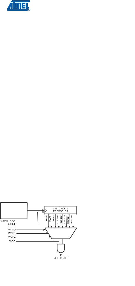
Watchdog Timer The Watchdog Timer is clocked from a separate On-chip Oscillator which runs at 1 MHz. This is the typical value at VCC = 5V. See characterization data for typical values at other VCC levels. By controlling the Watchdog Timer prescaler, the Watchdog Reset interval can be adjusted as shown in Table 17 on page 43. The WDR – Watchdog Reset – instruction resets the Watchdog Timer. The Watchdog Timer is also reset when it is disabled and when a Chip Reset occurs. Eight different clock cycle periods can be selected to determine the reset period. If the reset period expires without another Watchdog Reset, the ATmega16 resets and executes from the Reset Vector. For timing details on the Watchdog Reset, refer to page 41.
To prevent unintentional disabling of the Watchdog, a special turn-off sequence must be followed when the Watchdog is disabled. Refer to the description of the Watchdog Timer Control Register for details.
Figure 21. Watchdog Timer
WATCHDOG
OSCILLATOR
42 ATmega16(L) 
2466P–AVR–08/07

 ATmega16(L)
Watchdog Timer
Control Register –
WDTCR
Bit |
7 |
6 |
5 |
4 |
3 |
2 |
1 |
0 |
|
|
– |
– |
– |
WDTOE |
WDE |
WDP2 |
WDP1 |
WDP0 |
WDTCR |
|
|
|
|
|
|
|
|
|
|
Read/Write |
R |
R |
R |
R/W |
R/W |
R/W |
R/W |
R/W |
|
Initial Value |
0 |
0 |
0 |
0 |
0 |
0 |
0 |
0 |
|
• Bits 7..5 – Res: Reserved Bits
These bits are reserved bits in the ATmega16 and will always read as zero.
• Bit 4 – WDTOE: Watchdog Turn-off Enable
This bit must be set when the WDE bit is written to logic zero. Otherwise, the Watchdog will not be disabled. Once written to one, hardware will clear this bit after four clock cycles. Refer to the description of the WDE bit for a Watchdog disable procedure.
• Bit 3 – WDE: Watchdog Enable
When the WDE is written to logic one, the Watchdog Timer is enabled, and if the WDE is written to logic zero, the Watchdog Timer function is disabled. WDE can only be cleared if the WDTOE bit has logic level one. To disable an enabled Watchdog Timer, the following procedure must be followed:
1.In the same operation, write a logic one to WDTOE and WDE. A logic one must be written to WDE even though it is set to one before the disable operation starts.
2.Within the next four clock cycles, write a logic 0 to WDE. This disables the Watchdog.
• Bits 2..0 – WDP2, WDP1, WDP0: Watchdog Timer Prescaler 2, 1, and 0
The WDP2, WDP1, and WDP0 bits determine the Watchdog Timer prescaling when the Watchdog Timer is enabled. The different prescaling values and their corresponding Timeout Periods are shown in Table 17.
Table 17. Watchdog Timer Prescale Select
|
|
|
Number of WDT |
Typical Time-out |
Typical Time-out |
|
WDP2 |
WDP1 |
WDP0 |
Oscillator Cycles |
at VCC = 3.0V |
at VCC = 5.0V |
|
0 |
0 |
0 |
16K |
(16,384) |
17.1 ms |
16.3 ms |
|
|
|
|
|
|
|
0 |
0 |
1 |
32K |
(32,768) |
34.3 ms |
32.5 ms |
|
|
|
|
|
|
|
0 |
1 |
0 |
64K |
(65,536) |
68.5 ms |
65 ms |
|
|
|
|
|
|
|
0 |
1 |
1 |
128K |
(131,072) |
0.14 s |
0.13 s |
|
|
|
|
|
|
|
1 |
0 |
0 |
256K |
(262,144) |
0.27 s |
0.26 s |
|
|
|
|
|
|
|
1 |
0 |
1 |
512K |
(524,288) |
0.55 s |
0.52 s |
|
|
|
|
|
|
|
1 |
1 |
0 |
1,024K |
(1,048,576) |
1.1 s |
1.0 s |
|
|
|
|
|
|
|
1 |
1 |
1 |
2,048K |
(2,097,152) |
2.2 s |
2.1 s |
|
|
|
|
|
|
|
43
2466P–AVR–08/07

The following code example shows one assembly and one C function for turning off the WDT. The example assumes that interrupts are controlled (for example by disabling interrupts globally) so that no interrupts will occur during execution of these functions.
Assembly Code Example
WDT_off:
; Reset WDT
WDR
; Write logical one to WDTOE and WDE in r16, WDTCR
ori r16, (1<<WDTOE)|(1<<WDE) out WDTCR, r16
; Turn off WDT ldi r16, (0<<WDE) out WDTCR, r16 ret
C Code Example
void WDT_off(void)
{
/* Reset WDT*/ _WDR();
/* Write logical one to WDTOE and WDE */ WDTCR |= (1<<WDTOE) | (1<<WDE);
/* Turn off WDT */ WDTCR = 0x00;
}
44 ATmega16(L) 
2466P–AVR–08/07