AVR / datasheets / max232
.pdf
|
MAX232, MAX232I |
|
|
DUAL EIA 232 DRIVERS/RECEIVERS |
|
|
|
|
|
SLLS047L − FEBRUARY 1989 − REVISED MARCH 2004 |
|
|
|
|
DMeets or Exceeds TIA/EIA-232-F and ITU Recommendation V.28
DOperates From a Single 5-V Power Supply With 1.0-mF Charge-Pump Capacitors
DOperates Up To 120 kbit/s
DTwo Drivers and Two Receivers
D±30-V Input Levels
DLow Supply Current . . . 8 mA Typical
DESD Protection Exceeds JESD 22
−2000-V Human-Body Model (A114-A)
DUpgrade With Improved ESD (15-kV HBM) and 0.1-mF Charge-Pump Capacitors is
Available With the MAX202
DApplications
−TIA/EIA-232-F, Battery-Powered Systems, Terminals, Modems, and Computers
MAX232 . . . D, DW, N, OR NS PACKAGE MAX232I . . . D, DW, OR N PACKAGE
|
(TOP VIEW) |
|
|
||
C1+ |
|
|
|
|
VCC |
|
1 |
16 |
|
||
|
|
||||
VS+ |
|
2 |
15 |
|
GND |
|
|
||||
|
|
|
|
T1OUT |
|
C1− |
|
3 |
14 |
|
|
C2+ |
|
4 |
13 |
|
R1IN |
|
|
||||
C2− |
|
5 |
12 |
|
R1OUT |
|
|
||||
VS− |
|
6 |
11 |
|
T1IN |
|
|
||||
|
|
|
|
T2IN |
|
T2OUT |
|
7 |
10 |
|
|
R2IN |
|
8 |
9 |
|
R2OUT |
|
|
||||
|
|
|
|
|
|
description/ordering information
The MAX232 is a dual driver/receiver that includes a capacitive voltage generator to supply TIA/EIA-232-F voltage levels from a single 5-V supply. Each receiver converts TIA/EIA-232-F inputs to 5-V TTL/CMOS levels. These receivers have a typical threshold of 1.3 V, a typical hysteresis of 0.5 V, and can accept ±30-V inputs. Each driver converts TTL/CMOS input levels into TIA/EIA-232-F levels. The driver, receiver, and voltage-generator functions are available as cells in the Texas Instruments LinASIC library.
ORDERING INFORMATION
T |
|
PACKAGE† |
ORDERABLE |
TOP-SIDE |
||
|
|
|
||||
A |
|
|
|
PART NUMBER |
MARKING |
|
|
|
|
|
|||
|
PDIP (N) |
|
Tube of 25 |
MAX232N |
MAX232N |
|
|
|
|
|
|
|
|
|
SOIC (D) |
|
Tube of 40 |
MAX232D |
MAX232 |
|
|
|
|
|
|||
0°C to 70°C |
|
Reel of 2500 |
MAX232DR |
|||
|
|
|
||||
|
|
|
|
|
||
SOIC (DW) |
Tube of 40 |
MAX232DW |
MAX232 |
|||
|
||||||
|
|
|
||||
|
Reel of 2000 |
MAX232DWR |
||||
|
|
|
|
|||
|
|
|
|
|
|
|
|
SOP (NS) |
|
Reel of 2000 |
MAX232NSR |
MAX232 |
|
|
|
|
|
|
|
|
|
PDIP (N) |
|
Tube of 25 |
MAX232IN |
MAX232IN |
|
|
|
|
|
|
|
|
|
SOIC (D) |
|
Tube of 40 |
MAX232ID |
MAX232I |
|
−40 °C to 85°C |
|
|
|
|||
|
Reel of 2500 |
MAX232IDR |
||||
|
|
|
||||
|
|
|
|
|
|
|
|
SOIC (DW) |
Tube of 40 |
MAX232IDW |
MAX232I |
||
|
|
|
||||
|
Reel of 2000 |
MAX232IDWR |
||||
|
|
|
|
|||
|
|
|
|
|
|
|
†Package drawings, standard packing quantities, thermal data, symbolization, and PCB design guidelines are available at www.ti.com/sc/package.
Please be aware that an important notice concerning availability, standard warranty, and use in critical applications of Texas Instruments semiconductor products and disclaimers thereto appears at the end of this data sheet.
LinASIC is a trademark of Texas Instruments.
PRODUCTION DATA information is current as of publication date. |
Copyright 2004, Texas Instruments Incorporated |
Products conform to specifications per the terms of Texas Instruments |
|
standard warranty. Production processing does not necessarily include |
|
testing of all parameters. |
|
POST OFFICE BOX 655303 • DALLAS, TEXAS 75265 |
1 |
MAX232, MAX232I |
|
||||||||||||
DUAL EIA 232 DRIVERS/RECEIVERS |
|
|
|
|
|
|
|
|
|
|
|||
|
|
|
|
|
|
|
|
|
|
|
|
|
|
SLLS047L − FEBRUARY 1989 − REVISED MARCH 2004 |
|
|
|
|
|
|
|
|
|
|
|||
|
|
|
|
|
|
|
|
|
|
|
|
|
|
|
|
|
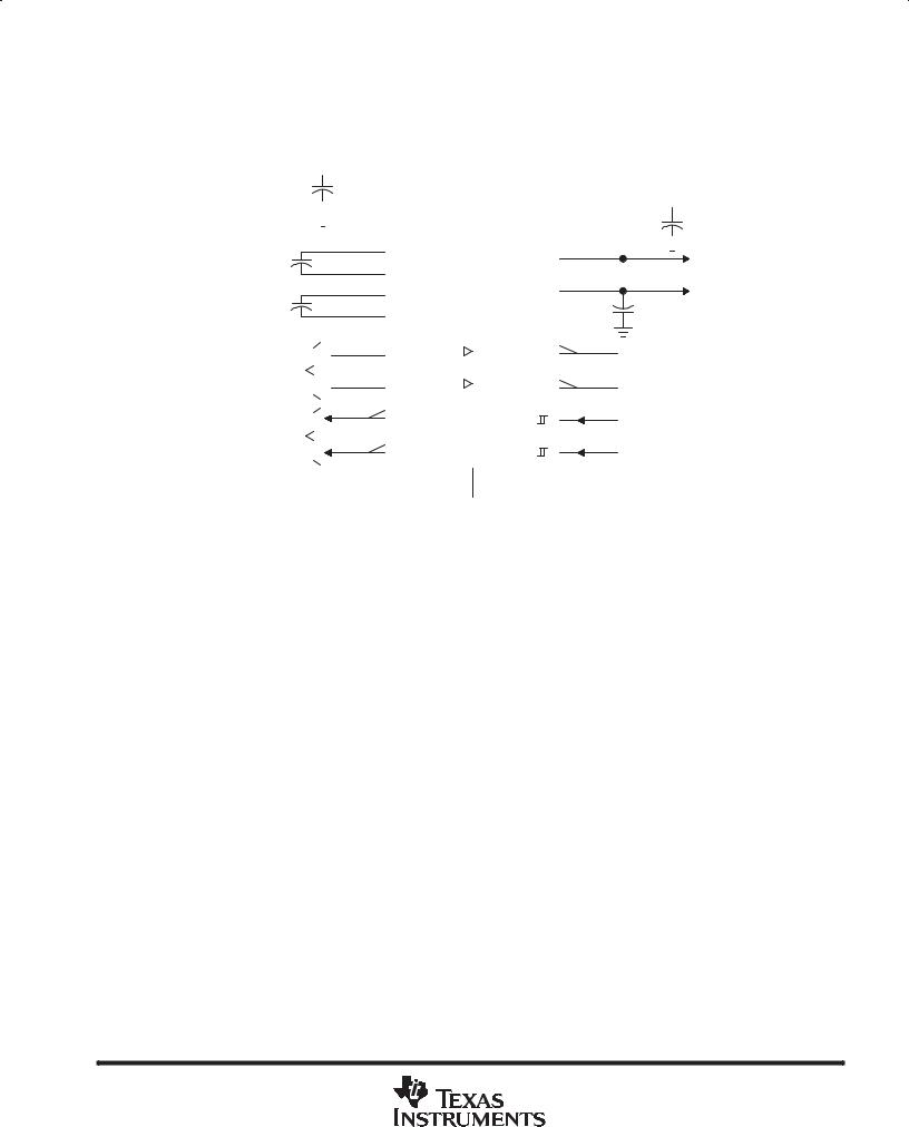
Function Tables |
||||||||||
|
|
|
EACH DRIVER |
||||||||||
|
|
|
|
|
|
|
|
|
|
|
|
|
|
|
|
|
INPUT |
OUTPUT |
|
|
|
||||||
|
|
|
TIN |
|
TOUT |
|
|
|
|||||
|
|
|
|
|
|
|
|
|
|
|
|
|
|
|
|
|
L |
|
|
|
|
|
|
H |
|
|
|
|
|
|
H |
|
|
|
|
|
|
L |
|
|
|
|
|
|
|
|
|
|
|
|
|
|
|
|
|
|
|
H = high level, L = low |
|||||||||||
|
|
level |
|
|
|
|
|
|
|
|
|
|
|
|
|
|
EACH RECEIVER |
||||||||||
|
|
|
|
|
|
|
|
|
|
|
|
|
|
|
|
|
INPUT |
OUTPUT |
|
|
|
||||||
|
|
|
RIN |
|
ROUT |
|
|
|
|||||
|
|
|
|
|
|
|
|
|
|
|
|
|
|
|
|
|
L |
|
|
|
|
|
|
H |
|
|
|
|
|
|
H |
|
|
|
|
|
|
L |
|
|
|
|
|
|
|
|
|
|
|
|
|
|
|
|
|
|
|
H = high level, L = low |
|||||||||||
|
|
level |
|
|
|
|
|
|
|
|
|
|
|
logic diagram (positive logic) |
|
|
|
|
|
|
|
|
|
|
|||
11 |
|
14 |
|
|
|||||||||
T1IN |
|
|
|
|
|
|
|
|
|
|
T1OUT |
||
|
7 |
||||||||||||
10 |
|
|
|
||||||||||
T2IN |
|
|
|
|
|
|
|
|
|
|
T2OUT |
||
|
13 |
||||||||||||
12 |
|
|
|
||||||||||
R1OUT |
|
|
|
|
|
|
|
|
|
|
R1IN |
||
9 |
|
8 |
|
|
|||||||||
R2OUT |
|
|
|
|
|
|
|
|
|
|
R2IN |
||
2 |
POST OFFICE BOX 655303 • DALLAS, TEXAS 75265 |

|
MAX232, MAX232I |
|
|
DUAL EIA 232 DRIVERS/RECEIVERS |
|
|
|
|
|
SLLS047L − FEBRUARY 1989 − REVISED MARCH 2004 |
|
|
|
|
absolute maximum ratings over operating free-air temperature range (unless otherwise noted)†
Input supply voltage range, VCC (see Note 1) . . . . . . . . . . . . . . . . . . . . . . . . . . . . . . . |
. . . . . . . . . . . −0.3 V to 6 V |
|
Positive output supply voltage range, VS+ . . . . . . . . . . . . . . . . . . . . . . . . . . . . . . . . . . |
. . . . . VCC − 0.3 V to 15 V |
|
Negative output supply voltage range, VS− . . . . . . . . . . . . . . . . . . . . . . . . . . . . . . . . . |
. . . . . . . . . −0.3 V to −15 V |
|
Input voltage range, VI: Driver . . . . . . . . . . . . . . . . . . . . . . . . . . . . . . . . . . . . . . . . . . . . |
. . . . −0.3 V to VCC + 0.3 |
V |
Receiver . . . . . . . . . . . . . . . . . . . . . . . . . . . . . . . . . . . . . . . . . |
. . . . . . . . . . . . . . . . . . ±30 |
V |
Output voltage range, VO: T1OUT, T2OUT . . . . . . . . . . . . . . . . . . . . . . . . . . . . . . . . |
VS− − 0.3 V to V S+ + 0.3 |
V |
R1OUT, R2OUT . . . . . . . . . . . . . . . . . . . . . . . . . . . . . . . . |
. . . . −0.3 V to V CC + 0.3 V |
|
Short-circuit duration: T1OUT, T2OUT . . . . . . . . . . . . . . . . . . . . . . . . . . . . . . . . . . . . |
. . . . . . . . . . . . . . . Unlimited |
|
Package thermal impedance, θJA (see Notes 2 and 3): D package . . . . . . . . . . . . |
. . . . . . . . . . . . . . . . 73°C/W |
|
DW package . . . . . . . . . . |
. . . . . . . . . . . . . . . . 57°C/W |
|
N package . . . . . . . . . . . . |
. . . . . . . . . . . . . . . . 67°C/W |
|
NS package . . . . . . . . . . . |
. . . . . . . . . . . . . . . . 64°C/W |
|
Operating virtual junction temperature, TJ . . . . . . . . . . . . . . . . . . . . . . . . . . . . . . . . . . |
. . . . . . . . . . . . . . . . . 150°C |
|
Storage temperature range, Tstg . . . . . . . . . . . . . . . . . . . . . . . . . . . . . . . . . . . . . . . . . . |
. . . . . . . . −65 °C to 150°C |
|
†Stresses beyond those listed under “absolute maximum ratings” may cause permanent damage to the device. These are stress ratings only, and functional operation of the device at these or any other conditions beyond those indicated under “recommended operating conditions” is not implied. Exposure to absolute-maximum-rated conditions for extended periods may affect device reliability.
NOTES: 1. All voltages are with respect to network GND.
2.Maximum power dissipation is a function of TJ(max), θJA, and TA. The maximum allowable power dissipation at any allowable ambient temperature is PD = (TJ(max) − T A)/θJA. Operating at the absolute maximum TJ of 150°C can affect reliability.
3.The package thermal impedance is calculated in accordance with JESD 51-7.
recommended operating conditions
|
|
|
MIN |
NOM |
MAX |
UNIT |
|
|
|
|
|
|
|
VCC |
Supply voltage |
4.5 |
5 |
5.5 |
V |
|
VIH |
High-level input voltage (T1IN,T2IN) |
2 |
|
|
V |
|
VIL |
Low-level input voltage (T1IN, T2IN) |
|
|
0.8 |
V |
|
R1IN, R2IN |
Receiver input voltage |
|
|
±30 |
V |
|
TA |
Operating free-air temperature |
MAX232 |
0 |
|
70 |
°C |
|
|
|
|
|||
MAX232I |
−40 |
|
85 |
|||
|
|
|
|
|||
|
|
|
|
|
|
|
electrical characteristics over recommended ranges of supply voltage and operating free-air temperature (unless otherwise noted) (see Note 4 and Figure 4)
|
|
PARAMETER |
|
TEST CONDITIONS |
MIN TYP‡ |
MAX |
UNIT |
|
|
ICC |
Supply current |
|
|
VCC = 5.5 V, All outputs open, |
8 |
10 |
mA |
|
|
|
TA = 25°C |
|||||
|
|
|
|
|
|
|
|
|
|
‡ All typical values are at V |
= 5 V and T |
= 25°C. |
|
|
|
||
|
|
CC |
A |
|
|
|
|
|
NOTE 4: |
Test conditions are C1−C4 = 1 µF at VCC = 5 V ± 0.5 V. |
|
|
|
||||
POST OFFICE BOX 655303 • DALLAS, TEXAS 75265 |
3 |

MAX232, MAX232I |
|
DUAL EIA 232 DRIVERS/RECEIVERS |
|
|
|
SLLS047L − FEBRUARY 1989 − REVISED MARCH 2004 |
|
|
|
|
DRIVER SECTION |
electrical characteristics over recommended ranges of supply voltage and operating free-air temperature range (see Note 4)
|
PARAMETER |
|
|
|
TEST CONDITIONS |
MIN |
TYP† |
MAX |
UNIT |
|
VOH |
High-level output voltage |
T1OUT, T2OUT |
RL = 3 kΩ to GND |
|
5 |
7 |
|
V |
||
V |
Low-level output voltage‡ |
T1OUT, T2OUT |
R |
L |
= 3 kΩ to GND |
|
|
−7 |
−5 |
V |
OL |
|
|
|
|
|
|
|
|
|
|
ro |
Output resistance |
T1OUT, T2OUT |
VS+ = VS− = 0, |
VO = ±2 V |
300 |
|
|
Ω |
||
IOS§ |
Short-circuit output current |
T1OUT, T2OUT |
VCC = 5.5 V, |
VO = 0 |
|
±10 |
|
mA |
||
IIS |
Short-circuit input current |
T1IN, T2IN |
VI = 0 |
|
|
|
200 |
µA |
||
†All typical values are at VCC = 5 V, TA = 25°C.
‡The algebraic convention, in which the least-positive (most negative) value is designated minimum, is used in this data sheet for logic voltage levels only.
§ Not more than one output should be shorted at a time.
NOTE 4: Test conditions are C1−C4 = 1 µF at VCC = 5 V ± 0.5 V.
switching characteristics, VCC = 5 V, TA = 25°C (see Note 4)
|
PARAMETER |
TEST CONDITIONS |
MIN TYP MAX |
UNIT |
|
|
|
|
|
|
|
SR |
Driver slew rate |
RL = 3 kΩ to 7 kΩ, |
30 |
V/µs |
|
See Figure 2 |
|||||
|
|
|
|
||
|
|
|
|
|
|
SR(t) |
Driver transition region slew rate |
See Figure 3 |
3 |
V/µs |
|
|
|
|
|
|
|
|
Data rate |
One TOUT switching |
120 |
kbit/s |
|
|
|
|
|
|
NOTE 4: Test conditions are C1−C4 = 1 µF at VCC = 5 V ± 0.5 V.
RECEIVER SECTION
electrical characteristics over recommended ranges of supply voltage and operating free-air temperature range (see Note 4)
|
PARAMETER |
|
TEST CONDITIONS |
MIN |
TYP† |
MAX |
UNIT |
||
VOH |
High-level output voltage |
R1OUT, R2OUT |
IOH = −1 mA |
|
3.5 |
|
|
V |
|
VOL |
Low-level output voltage‡ |
R1OUT, R2OUT |
IOL = 3.2 mA |
|
|
|
0.4 |
V |
|
VIT+ |
Receiver positive-going input |
R1IN, R2IN |
VCC = 5 |
V, |
TA = 25°C |
|
1.7 |
2.4 |
V |
threshold voltage |
|
||||||||
|
|
|
|
|
|
|
|
|
|
|
|
|
|
|
|
|
|
|
|
VIT− |
Receiver negative-going input |
R1IN, R2IN |
VCC = 5 |
V, |
TA = 25°C |
0.8 |
1.2 |
|
V |
threshold voltage |
|
||||||||
|
|
|
|
|
|
|
|
|
|
|
|
|
|
|
|
|
|
|
|
Vhys |
Input hysteresis voltage |
R1IN, R2IN |
VCC = 5 |
V |
|
0.2 |
0.5 |
1 |
V |
ri |
Receiver input resistance |
R1IN, R2IN |
VCC = 5, |
|
TA = 25°C |
3 |
5 |
7 |
kΩ |
†All typical values are at VCC = 5 V, TA = 25°C.
‡ The algebraic convention, in which the least-positive (most negative) value is designated minimum, is used in this data sheet for logic voltage levels only.
NOTE 4: Test conditions are C1−C4 = 1 µF at VCC = 5 V ± 0.5 V.
switching characteristics, VCC = 5 V, TA = 25°C (see Note 4 and Figure 1)
|
PARAMETER |
TYP |
UNIT |
|
|
|
|
tPLH(R) |
Receiver propagation delay time, lowto high-level output |
500 |
ns |
tPHL(R) |
Receiver propagation delay time, highto low-level output |
500 |
ns |
NOTE 4: Test conditions are C1−C4 = 1 µF at VCC = 5 V ± 0.5 V.
4 |
POST OFFICE BOX 655303 • DALLAS, TEXAS 75265 |
|
MAX232, MAX232I |
|
DUAL EIA 232 DRIVERS/RECEIVERS |
|
|
|
|
|
|
|
|
SLLS047L − FEBRUARY 1989 − REVISED MARCH 2004 |
|
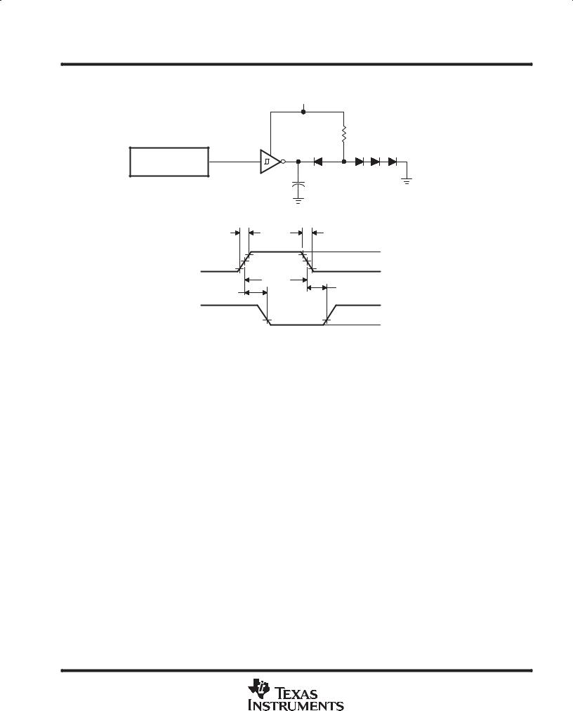
PARAMETER MEASUREMENT INFORMATION |
|||||
|
|
|
|
VCC |
|
|
|
|
R1IN |
|
R1OUT |
RL = 1.3 kΩ |
|
|
|
|
or |
|
|
|
|
|
or |
|
|
See Note C |
|
Pulse |
|
|
R2OUT |
|
||
|
R2IN |
|
|
|||
Generator |
|
|
|
|
||
|
|
|
|
|
||
(see Note A) |
|
|
|
|
|
|
|
|
|
|
|
CL = 50 pF |
|
|
|
|
|
|
(see Note B) |
|
|
|
|
TEST CIRCUIT |
|
|
|
|
≤10 ns |
|
|
≤10 ns |
|
|
|
|
|
90% |
90% |
|
3 V |
|
Input |
|
|
|
||
|
10% |
50% |
50% |
10% |
|
|
|
|
0 V |
||||
|
|
|
500 ns |
|
||
|
|
|
tPLH |
|
||
|
|
tPHL |
|
|
|
|
|
|
|
|
|
|
|
|
Output |
|
|
|
|
VOH |
|
1.5 V |
1.5 V |
VOL |
|||
|
|
|||||
|
|
|
|
|
|
|
WAVEFORMS
NOTES: A. The pulse generator has the following characteristics: ZO = 50 Ω, duty cycle ≤ 50%.
B.CL includes probe and jig capacitance.
C.All diodes are 1N3064 or equivalent.
Figure 1. Receiver Test Circuit and Waveforms for tPHL and tPLH Measurements
POST OFFICE BOX 655303 • DALLAS, TEXAS 75265 |
5 |
MAX232, MAX232I |
|
|
|
|
|
|
|
|
|
|
|
|
|
|
|
|
|
|
|
|
|
|
DUAL EIA 232 DRIVERS/RECEIVERS |
|
|
|
|
|
|
|
|
|
|
|
|
|
|||||||||
|
|
|
|
|
|
|
|
|
|
|
|
|
|
|
|
|
|
|
|
|
|
|
SLLS047L − FEBRUARY 1989 − REVISED MARCH 2004 |
|
|
|
|
|
|
|
|
|
|
|
|
|
|
||||||||
|
|
|
|
|
|
|
|
|
|
|
|
|
|
|
|
|
|
|
|
|||
|
|
|
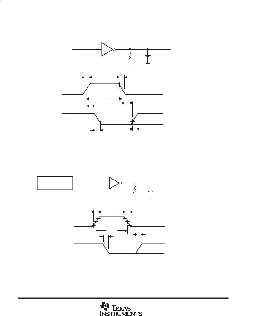
PARAMETER MEASUREMENT INFORMATION |
|||||||||||||||||||
|
|
|
T1IN or T2IN |
|
T1OUT or T2OUT |
|
||||||||||||||||
|
Pulse |
|
|
EIA-232 Output |
||||||||||||||||||
|
|
|
|
|
|
|
|
|
|
|
|
|
|
|
|
|
|
|
|
|
||
|
Generator |
|
|
|
|
|
|
|
|
|
|
|
|
|
|
|
|
|
|
|
|
|
|
(see Note A) |
|
|
|
|
|
|
|
|
|
RL |
|
|
|
|
|
|
|
CL = 10 pF |
|||
|
|
|
|
|
|
|
|
|
|
|
|
|
|
|
|
|||||||
|
|
|
|
|
|
|
|
|
|
|
|
|
|
|
|
|||||||
|
|
|
|
|
|
|
|
|
|
|
|
|
|
|
|
|
|
|||||
|
|
|
|
|
|
|
|
|
|
|
|
|
|
|
|
|
|
|||||
|
|
|
|
|
|
|
|
|
|
|
|
|
|
|
|
|
|
|
|
|
|
(see Note B) |
|
|
|
|
|
|
|
|
|
|
|
|
|
|
|
|
|
||||||
|
|
|
|
|
|
|
|
|
TEST CIRCUIT |
|
||||||||||||
|
|
≤10 ns |
|
|
|
|
|
|
|
|
|
|
|
|
|
|
≤10 ns |
|
||||
|
|
|
|
90% |
90% |
|
|
|
|
|
|
|
|
|
|
|
3 V |
|||||
|
Input |
|
|
|
|
|
|
|
|
|
|
|
|
|
|
|||||||
|
10% |
50% |
|
|
50% |
|
|
|
|
|
|
|
|
|
|
|
||||||
|
|
|
|
|
|
|
|
|
|
|
|
|
|
|
||||||||
|
|
|
|
|
|
|
|
10% |
|
|
|
0 V |
||||||||||
|
|
|
|
|
|
|
|
|
|
|
|
|
|
|
|
|
|
|
|
|
|
|
|
|
|
|
|
|
|
|
|
5 µs |
|
|
|
|
|
|
|
|
|
|
|
|
|
|
|
tPHL |
|
|
|
|
|
|
|
|
|
|
|
|
|
|
tPLH |
|
||||
|
|
|
|
|
|
|
|
|
|
|
|
|
|
|
|
|
|
|
|
|
||
|
Output |
|
|
|
|
|
|
90% |
90% |
|
|
VOH |
||||||||||
|
|
|
|
|
|
|
|
|
||||||||||||||
|
|
|
|
|
|
|
||||||||||||||||
|
|
|
|
|
|
|
|
|
|
|
|
|||||||||||
|
|
|
|
|
|
|
|
10% |
10% |
|
|
|
|
|
|
|
|
|
|
|||
|
|
|
|
|
|
|
|
|
|
|
|
|
|
|
|
|
|
VOL |
||||
|
|
|
|
|
|
|
|
|
|
|
|
|
|
|
|
|
|
tTLH |
||||
|
|
|
tTHL |
|
|
|
|
|
|
|
|
|
|
|
|
|
|
|
||||
|
|
|
SR + |
|
0.8 (VOH – V OL) |
or |
0.8 (VOL – V OH) |
|
|
|
||||||||||||
|
|
|
|
|
|
|
|
|
tTHL |
|
||||||||||||
|
|
|
|
|
|
|
|
|
tTLH |
|
|
|
|
|
|
|
|
|
||||
WAVEFORMS
NOTES: A. The pulse generator has the following characteristics: ZO = 50 Ω, duty cycle ≤ 50%.
B. CL includes probe and jig capacitance.
Figure 2. Driver Test Circuit and Waveforms for tPHL and tPLH Measurements (5- s Input)
Pulse
Generator 
 EIA-232 Output
(see Note A)
|
|
|
|
|
|
|
|
|
|
3 kΩ |
|
|
|
|
|
|
|
|
|
|
|
|
|
CL = 2.5 nF |
|
|
|
|
|
|
|
|
TEST CIRCUIT |
|
|
|
|
|
|
|
|
|
|
|
|
|
|
||
|
|
|
|
|
|
|
|
|
|
|
|
|
|
|
|
|
|
|
|
|
|
|||
|
|
|
|
|
|
|
|
|
|
|
|
|
|
|
|
|
|
|
|
|
|
|||
|
≤10 ns |
|
|
|
|
|
|
|
|
|
|
|
|
|
|
|
≤10 ns |
|
||||||
Input |
|
90% |
90% |
|
|
|
|
|
|
|
|
|
|
|
|
|
|
|||||||
|
|
|
|
|
|
|
|
|
|
|
|
|
|
|
|
|||||||||
|
10% |
1.5 V |
|
|
1.5 V |
10% |
|
|
|
|
|
|||||||||||||
|
|
|
|
|
|
|
|
|
|
|
|
|
|
|
||||||||||
|
|
|
|
|
|
20 µs |
|
|
|
|
|
|
|
|
|
|
|
|
|
|
||||
|
|
tTHL |
|
|
|
|
|
|
|
|
|
|
|
|
|
|
tTLH |
|
||||||
|
|
|
|
|
|
|
|
|
|
|
|
|
|
|
|
|
|
|
|
|||||
|
|
|
|
|
|
|
|
|
|
|
|
|
|
|
|
|
|
|
|
|
|
|
|
VOH |
|
|
|
|
|
|
|
|
|
|
|
|
|
|
|
|
|
|
|
|
|
|
|
|
|
Output |
|
3 V |
|
|
|
|
|
|
−3 V |
|
|
|
|
|
|
|
|
|
|
3 V |
||||
|
|
|
|
|
|
|
|
|
|
|
|
|
|
|
|
|
||||||||
|
|
−3 V |
|
|
|
6 V |
|
|
|
|
|
|
|
|
|
|
|
|
|
VOL |
||||
|
|
|
|
SR + |
|
|
|
|
|
|
|
|
|
|
|
|
|
|
||||||
|
|
|
|
tTHL or tTLH |
|
|
|
|
||||||||||||||||
WAVEFORMS
NOTE A: The pulse generator has the following characteristics: ZO = 50 Ω, duty cycle ≤ 50%.
Figure 3. Test Circuit and Waveforms for tTHL and tTLH Measurements (20- s Input)
6 |
POST OFFICE BOX 655303 • DALLAS, TEXAS 75265 |
|
|
|
|
|
|
|
|
|
|
|
|
|
|
|
|
|
|
|
|
|
|
|
|
MAX232, MAX232I |
|
|
|
|
|
|
|
|
|
|
|
|
|
|
DUAL EIA 232 DRIVERS/RECEIVERS |
||||||||||||
|
|
|
|
|
|
|
|
|
|
|
|
|
|
|
|
|
|
|
|
|
|
|
|
||
|
|
|
|
|
|
|
|
|
|
|
|
|
|
SLLS047L − FEBRUARY 1989 − REVISED MARCH 2004 |
|||||||||||
|
|
|
|
|
|
|
|
|
|
|
|
|
|
|
|
|
|
|
|
|
|
|
|
|
|
|
|
|
|
|
|
|
|
APPLICATION INFORMATION |
|
|
|
|
|
|
|
|
|
|
|
||||||
|
|
|
|
|
|
|
|
|
|
5 V |
|
|
|
|
|
|
|
|
|
|
|
||||
CBYPASS =1 F |
+ |
|
|
|
|
|
|
|
|
|
|
|
|
|
|
|
|
|
|
|
|
|
|||
|
|
|
|
|
|
|
|
|
|
|
|
|
|
|
|
|
|
|
|
|
|||||
|
|
|
|
|
|
|
|
|
|
|
|
|
|
|
|
|
|
|
|
|
|||||
− |
|
|
|
|
|
|
|
|
|
|
|
|
|
|
|
|
|
|
|
|
|
||||
|
|
|
|
|
|
|
|
16 |
|
|
|
|
|
|
|
|
|
|
|
|
|
|
|||
|
|
|
|
|
|
|
|
|
|
|
|
|
|
|
|
|
|
|
|
|
|
|
|
|
|
|
|
|
|
|
|
|
|
|
|
|
|
|
|
|
|
C3† |
|
|
|
|
|
|
1 F |
||
|
|
|
|
|
|
|
|
|
|
|
|
|
|
|
|
|
|
|
|
||||||
|
|
|
|
|
|
|
|
1 |
C1+ |
VCC |
2 |
|
|
||||||||||||
C1 |
|
|
1 F |
|
|
|
|
|
|
|
|
|
8.5 V |
||||||||||||
|
|
|
|
|
|
|
|
|
|
|
|
|
|
||||||||||||
|
|
|
|
|
|
|
|
|
|
|
|||||||||||||||
|
|
3 |
|
VS+ |
|
|
|
|
|
|
|
|
|
|
|||||||||||
|
|
C1− |
|
|
|
|
|
|
|
|
|
|
|
||||||||||||
|
|
|
|
|
|
|
|
|
|
|
|
|
|
|
|||||||||||
|
|
|
|
|
|
|
|
4 |
|
|
|
|
6 |
|
|
|
|
|
|
|
|
|
−8.5 V |
||
|
|
|
|
|
|
|
|
|
|
|
|
|
|
|
|
|
|
|
|
|
|||||
|
|
|
|
|
|
|
|
C2+ |
|
VS− |
|
|
|
|
|
|
|
|
|
|
|||||
C2 |
|
|
1 F |
5 |
|
C4 |
|
|
1 F |
|
|||||||||||||||
|
|
|
+ |
|
|
|
|
||||||||||||||||||
|
|
C2− |
|
|
|
|
|
|
|
|
|||||||||||||||
|
|
|
|
|
|
|
|
11 |
|
|
|
|
14 |
|
|
|
|
|
|
|
|
|
|
||
|
|
|
|
|
|
|
|
|
|
|
|
|
EIA-232 Output |
||||||||||||
|
|
|
|
|
|
|
|
|
|
|
|
|
|||||||||||||
|
|
|
|
|
|
|
|
|
|
|
|
|
|
||||||||||||
|
|
|
|
|
|
|
|
|
|
|
|
|
|
||||||||||||
|
|
|
|
|
|
|
|
|
|
|
|
|
|
|
|
||||||||||
From CMOS or TTL |
|
|
|
|
|
|
10 |
|
|
|
|
|
7 |
|
EIA-232 Output |
||||||||||
|
|
|
|
|
|
|
|
|
|
|
|
||||||||||||||
|
|
|
|
|
|
|
|
|
|
|
|
||||||||||||||
|
|
|
|
|
|
|
|
|
|
|
|
|
|||||||||||||
|
|
|
|
|
|
|
|
|
|
|
|
|
|
|
|
||||||||||
To CMOS or TTL |
|
|
|
|
|
|
12 |
|
|
|
|
|
13 |
|
EIA-232 Input |
||||||||||
|
|
|
|
|
|
|
|
|
|
|
|
||||||||||||||
|
|
|
|
|
|
9 |
|
|
|
|
|
8 |
|
EIA-232 Input |
|||||||||||
|
|
|
|
|
|
|
|
|
|
0 V |
|
|
|
|
|
|
|
|
|
|
|
|
|||
|
|
|
|
|
|
|
|
|
|
15 |
|
|
|
|
|
|
|
|
|
|
|
|
|
|
|
GND
†C3 can be connected to VCC or GND.
NOTES: A. Resistor values shown are nominal.
B.Nonpolarized ceramic capacitors are acceptable. If polarized tantalum or electrolytic capacitors are used, they should be connected as shown. In addition to the 1- F capacitors shown, the MAX202 can operate with 0.1- F capacitors.
Figure 4. Typical Operating Circuit
POST OFFICE BOX 655303 • DALLAS, TEXAS 75265 |
7 |