

- •Features
- •Pin Configurations
- •Overview
- •Block Diagram
- •Pin Descriptions
- •Port A (PA7..PA0)
- •Port B (PB7..PB0)
- •Port C (PC7..PC0)
- •Port D (PD7..PD0)
- •Port E (PE7..PE0)
- •Port F (PF7..PF0)
- •Port G (PG4..PG0)
- •RESET
- •XTAL1
- •XTAL2
- •AVCC
- •AREF
- •AVR CPU Core
- •Introduction
- •Architectural Overview
- •Status Register
- •Stack Pointer
- •Interrupt Response Time
- •SRAM Data Memory
- •Data Memory Access Times
- •EEPROM Data Memory
- •EEPROM Read/Write Access
- •I/O Memory
- •Overview
- •ATmega103 Compatibility
- •Address Latch Requirements
- •Pull-up and Bus-keeper
- •Timing
- •XMEM Register Description
- •Using all Locations of External Memory Smaller than 64 KB
- •Using all 64KB Locations of External Memory
- •Clock Systems and their Distribution
- •CPU Clock – clkCPU
- •I/O Clock – clkI/O
- •Flash Clock – clkFLASH
- •ADC Clock – clkADC
- •Clock Sources
- •Default Clock Source
- •Crystal Oscillator
- •External RC Oscillator
- •External Clock
- •Timer/Counter Oscillator
- •Idle Mode
- •Power-down Mode
- •Power-save Mode
- •Standby Mode
- •Extended Standby Mode
- •Analog to Digital Converter
- •Analog Comparator
- •Brown-out Detector
- •Internal Voltage Reference
- •Watchdog Timer
- •Port Pins
- •Resetting the AVR
- •Reset Sources
- •Power-on Reset
- •External Reset
- •Brown-out Detection
- •Watchdog Reset
- •Watchdog Timer
- •Timed Sequences for Changing the Configuration of the Watchdog Timer
- •Safety Level 0
- •Safety Level 1
- •Safety Level 2
- •Interrupts
- •I/O Ports
- •Introduction
- •Configuring the Pin
- •Reading the Pin Value
- •Unconnected pins
- •Alternate Port Functions
- •Alternate Functions of Port A
- •Alternate Functions of Port B
- •Alternate Functions of Port C
- •Alternate Functions of Port D
- •Alternate Functions of Port E
- •Alternate Functions of Port F
- •Alternate Functions of Port G
- •Register Description for I/O Ports
- •Port A Data Register – PORTA
- •Port B Data Register – PORTB
- •Port C Data Register – PORTC
- •Port D Data Register – PORTD
- •Port E Data Register – PORTE
- •Port F Data Register – PORTF
- •Port G Data Register – PORTG
- •External Interrupts
- •8-bit Timer/Counter0 with PWM and Asynchronous Operation
- •Overview
- •Registers
- •Definitions
- •Counter Unit
- •Output Compare Unit
- •Force Output Compare
- •Modes of Operation
- •Normal Mode
- •Fast PWM Mode
- •Phase Correct PWM Mode
- •Timer/Counter Prescaler
- •16-bit Timer/Counter (Timer/Counter1 and Timer/Counter3)
- •Overview
- •Registers
- •Definitions
- •Compatibility
- •Counter Unit
- •Input Capture Unit
- •Input Capture Trigger Source
- •Noise Canceler
- •Using the Input Capture Unit
- •Output Compare Units
- •Force Output Compare
- •Modes of Operation
- •Normal Mode
- •Fast PWM Mode
- •Phase Correct PWM Mode
- •Internal Clock Source
- •Prescaler Reset
- •External Clock Source
- •8-bit Timer/Counter2 with PWM
- •Overview
- •Registers
- •Definitions
- •Counter Unit
- •Output Compare Unit
- •Force Output Compare
- •Modes of Operation
- •Normal Mode
- •Fast PWM Mode
- •Phase Correct PWM Mode
- •Overview
- •Description
- •Timing Example
- •Slave Mode
- •Master Mode
- •SPI Control Register – SPCR
- •SPI Status Register – SPSR
- •SPI Data Register – SPDR
- •Data Modes
- •USART
- •Dual USART
- •Overview
- •AVR USART vs. AVR UART – Compatibility
- •Clock Generation
- •External Clock
- •Synchronous Clock Operation
- •Frame Formats
- •Parity Bit Calculation
- •USART Initialization
- •Sending Frames with 5 to 8 Data Bit
- •Sending Frames with 9 Data Bit
- •Parity Generator
- •Disabling the Transmitter
- •Receiving Frames with 5 to 8 Data Bits
- •Receiving Frames with 9 Data Bits
- •Receiver Error Flags
- •Parity Checker
- •Disabling the Receiver
- •Flushing the Receive Buffer
- •Asynchronous Data Recovery
- •Using MPCM
- •Two-wire Serial Interface
- •Features
- •TWI Terminology
- •Electrical Interconnection
- •Transferring Bits
- •START and STOP Conditions
- •Address Packet Format
- •Data Packet Format
- •Overview of the TWI Module
- •Scl and SDA Pins
- •Bit Rate Generator Unit
- •Bus Interface Unit
- •Address Match Unit
- •Control Unit
- •TWI Register Description
- •TWI Bit Rate Register – TWBR
- •TWI Control Register – TWCR
- •TWI Status Register – TWSR
- •TWI Data Register – TWDR
- •Using the TWI
- •Transmission Modes
- •Master Transmitter Mode
- •Master Receiver Mode
- •Slave Receiver Mode
- •Slave Transmitter Mode
- •Miscellaneous States
- •Analog Comparator
- •Analog to Digital Converter
- •Features
- •Operation
- •Starting a Conversion
- •Differential Gain Channels
- •Changing Channel or Reference Selection
- •ADC Input Channels
- •ADC Voltage Reference
- •ADC Noise Canceler
- •Analog Input Circuitry
- •ADC Accuracy Definitions
- •ADC Conversion Result
- •ADLAR = 0:
- •ADLAR = 1:
- •Features
- •Overview
- •Test Access Port – TAP
- •TAP Controller
- •PRIVATE0; $8
- •PRIVATE1; $9
- •PRIVATE2; $A
- •PRIVATE3; $B
- •Bibliography
- •Features
- •System Overview
- •Data Registers
- •Bypass Register
- •Device Identification Register
- •Reset Register
- •Boundary-scan Chain
- •EXTEST; $0
- •IDCODE; $1
- •SAMPLE_PRELOAD; $2
- •AVR_RESET; $C
- •BYPASS; $F
- •Boundary-scan Chain
- •Scanning the Digital Port Pins
- •Scanning the RESET Pin
- •Scanning the Clock Pins
- •Scanning the ADC
- •Boot Loader Features
- •Application Section
- •Boot Loader Section – BLS
- •Boot Loader Lock Bits
- •Performing a Page Write
- •Using the SPM Interrupt
- •Setting the Boot Loader Lock Bits by SPM
- •Reading the Fuse and Lock Bits from Software
- •Preventing Flash Corruption
- •Simple Assembly Code Example for a Boot Loader
- •Fuse Bits
- •Latching of Fuses
- •Signature Bytes
- •Calibration Byte
- •Signal Names
- •Parallel Programming
- •Enter Programming Mode
- •Chip Erase
- •Programming the Flash
- •Programming the EEPROM
- •Reading the Flash
- •Reading the EEPROM
- •Programming the Lock Bits
- •Reading the Signature Bytes
- •Reading the Calibration Byte
- •Serial Downloading
- •Data Polling Flash
- •Data Polling EEPROM
- •AVR_RESET ($C)
- •PROG_ENABLE ($4)
- •PROG_COMMANDS ($5)
- •PROG_PAGELOAD ($6)
- •PROG_PAGEREAD ($7)
- •Data Registers
- •Reset Register
- •Programming Enable Register
- •Programming Command Register
- •Virtual Flash Page Read Register
- •Programming Algorithm
- •Entering Programming Mode
- •Leaving Programming Mode
- •Performing Chip Erase
- •Programming the Flash
- •Reading the Flash
- •Programming the EEPROM
- •Reading the EEPROM
- •Programming the Fuses
- •Programming the Lock Bits
- •Reading the Signature Bytes
- •Reading the Calibration Byte
- •Electrical Characteristics
- •Absolute Maximum Ratings*
- •DC Characteristics
- •External Clock Drive Waveforms
- •External Clock Drive
- •Two-wire Serial Interface Characteristics
- •ADC Characteristics – Preliminary Data
- •External Data Memory Timing
- •Ordering Information
- •Packaging Information
- •Errata
- •ATmega128 Rev. I
- •ATmega128 Rev. H
- •ATmega128 Rev. G
- •ATmega128 Rev. F
- •Datasheet Change Log for ATmega128
- •Changes from Rev. 2467J-12/03 to Rev. 2467K-03/04
- •Changes from Rev. 2467I-09/03 to Rev. 2467J-12/03
- •Changes from Rev. 2467H-02/03 to Rev. 2467I-09/03
- •Changes from Rev. 2467G-09/02 to Rev. 2467H-02/03
- •Changes from Rev. 2467F-09/02 to Rev. 2467G-09/02
- •Changes from Rev. 2467E-04/02 to Rev. 2467F-09/02
- •Changes from Rev. 2467D-03/02 to Rev. 2467E-04/02
- •Changes from Rev. 2467C-02/02 to Rev. 2467D-03/02
- •Changes from Rev. 2467B-09/01 to Rev. 2467C-02/02
- •Table of Contents
ATmega128
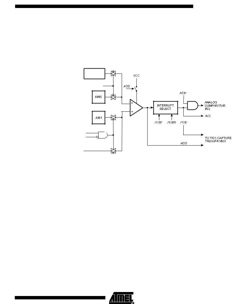
Analog Comparator The Analog Comparator compares the input values on the positive pin AIN0 and negative pin AIN1. When the voltage on the positive pin AIN0 is higher than the voltage on the negative pin AIN1, the Analog Comparator Output, ACO, is set. The comparator’s output can be set to trigger the Timer/Counter1 Input Capture function. In addition, the comparator can trigger a separate interrupt, exclusive to the Analog Comparator. The user can select Interrupt triggering on comparator output rise, fall or toggle. A block diagram of the comparator and its surrounding logic is shown in Figure 107.
Figure 107. Analog Comparator Block Diagram
BANDGAP
REFERENCE
ACBG
ACME
ADEN
ADC MULTIPLEXER
OUTPUT1)
Special Function IO Register –
SFIOR
Notes: 1. See Table 94 on page 231.
2.Refer to Figure 1 on page 2 and Table 30 on page 71 for Analog Comparator pin placement.
Bit |
7 |
6 |
5 |
4 |
3 |
2 |
1 |
0 |
|
|
TSM |
– |
– |
– |
ACME |
PUD |
PSR0 |
PSR321 |
SFIOR |
Read/Write |
R/W |
R |
R |
R |
R/W |
R/W |
R/W |
R/W |
|
Initial Value |
0 |
0 |
0 |
0 |
0 |
0 |
0 |
0 |
|
• Bit 3 – ACME: Analog Comparator Multiplexer Enable
Analog Comparator Control
and Status Register – ACSR
2467K–AVR–04/04
When this bit is written logic one and the ADC is switched off (ADEN in ADCSRA is zero), the ADC multiplexer selects the negative input to the Analog Comparator. When this bit is written logic zero, AIN1 is applied to the negative input of the Analog Comparator. For a detailed description of this bit, see “Analog Comparator Multiplexed Input” on page 230.
Bit |
7 |
6 |
5 |
4 |
3 |
2 |
1 |
0 |
|
|
ACD |
ACBG |
ACO |
ACI |
ACIE |
ACIC |
ACIS1 |
ACIS0 |
ACSR |
|
|
|
|
|
|
|
|
|
|
Read/Write |
R/W |
R/W |
R |
R/W |
R/W |
R/W |
R/W |
R/W |
|
Initial Value |
0 |
0 |
N/A |
0 |
0 |
0 |
0 |
0 |
|
• Bit 7 – ACD: Analog Comparator Disable
229

Analog Comparator
Multiplexed Input
When this bit is written logic one, the power to the Analog Comparator is switched off. This bit can be set at any time to turn off the Analog Comparator. This will reduce power consumption in Active and Idle mode. When changing the ACD bit, the Analog Comparator Interrupt must be disabled by clearing the ACIE bit in ACSR. Otherwise an interrupt can occur when the bit is changed.
• Bit 6 – ACBG: Analog Comparator Bandgap Select
When this bit is set, a fixed bandgap reference voltage replaces the positive input to the Analog Comparator. When this bit is cleared, AIN0 is applied to the positive input of the Analog Comparator. See “Internal Voltage Reference” on page 52.
• Bit 5 – ACO: Analog Comparator Output
The output of the Analog Comparator is synchronized and then directly connected to ACO. The synchronization introduces a delay of 1 – 2 clock cycles.
• Bit 4 – ACI: Analog Comparator Interrupt Flag
This bit is set by hardware when a comparator output event triggers the interrupt mode defined by ACIS1 and ACIS0. The Analog Comparator Interrupt routine is executed if the ACIE bit is set and the I-bit in SREG is set. ACI is cleared by hardware when executing the corresponding interrupt handling vector. Alternatively, ACI is cleared by writing a logic one to the flag.
• Bit 3 – ACIE: Analog Comparator Interrupt Enable
When the ACIE bit is written logic one and the I-bit in the Status Register is set, the Analog Comparator interrupt is activated. When written logic zero, the interrupt is disabled.
• Bit 2 – ACIC: Analog Comparator Input Capture Enable
When written logic one, this bit enables the Input Capture function in Timer/Counter1 to be triggered by the Analog Comparator. The comparator output is in this case directly connected to the Input Capture front-end logic, making the comparator utilize the noise canceler and edge select features of the Timer/Counter1 Input Capture interrupt. When written logic zero, no connection between the analog comparator and the Input Capture function exists. To make the comparator trigger the Timer/Counter1 Input Capture interrupt, the TICIE1 bit in the Timer Interrupt Mask Register (TIMSK) must be set.
• Bits 1, 0 – ACIS1, ACIS0: Analog Comparator Interrupt Mode Select
These bits determine which comparator events that trigger the Analog Comparator interrupt. The different settings are shown in Table 93.
Table 93. |
ACIS1/ACIS0 Settings |
||
ACIS1 |
|
ACIS0 |
Interrupt Mode |
|
|
|
|
0 |
|
0 |
Comparator Interrupt on Output Toggle |
|
|
|
|
0 |
|
1 |
Reserved |
|
|
|
|
1 |
|
0 |
Comparator Interrupt on Falling Output Edge |
|
|
|
|
1 |
|
1 |
Comparator Interrupt on Rising Output Edge |
|
|
|
|
When changing the ACIS1/ACIS0 bits, the Analog Comparator Interrupt must be disabled by clearing its Interrupt Enable bit in the ACSR Register. Otherwise an interrupt can occur when the bits are changed.
It is possible to select any of the ADC7..0 pins to replace the negative input to the Analog Comparator. The ADC multiplexer is used to select this input, and consequently, the ADC must be switched off to utilize this feature. If the Analog Comparator Multiplexer
230 ATmega128
2467K–AVR–04/04
 ATmega128
Enable bit (ACME in SFIOR) is set and the ADC is switched off (ADEN in ADCSRA is zero), MUX2..0 in ADMUX select the input pin to replace the negative input to the Analog Comparator, as shown in Table 94. If ACME is cleared or ADEN is set, AIN1 is applied to the negative input to the Analog Comparator.
Table 94. Analog Comparator Multiplexed Input
ACME |
ADEN |
MUX2..0 |
Analog Comparator Negative Input |
|
|
|
|
0 |
x |
xxx |
AIN1 |
|
|
|
|
1 |
1 |
xxx |
AIN1 |
|
|
|
|
1 |
0 |
000 |
ADC0 |
|
|
|
|
1 |
0 |
001 |
ADC1 |
|
|
|
|
1 |
0 |
010 |
ADC2 |
|
|
|
|
1 |
0 |
011 |
ADC3 |
|
|
|
|
1 |
0 |
100 |
ADC4 |
|
|
|
|
1 |
0 |
101 |
ADC5 |
|
|
|
|
1 |
0 |
110 |
ADC6 |
|
|
|
|
1 |
0 |
111 |
ADC7 |
|
|
|
|
231
2467K–AVR–04/04