

- •Features
- •Pin Configurations
- •Overview
- •Block Diagram
- •Pin Descriptions
- •Port A (PA7..PA0)
- •Port B (PB7..PB0)
- •Port C (PC7..PC0)
- •Port D (PD7..PD0)
- •Port E (PE7..PE0)
- •Port F (PF7..PF0)
- •Port G (PG4..PG0)
- •RESET
- •XTAL1
- •XTAL2
- •AVCC
- •AREF
- •AVR CPU Core
- •Introduction
- •Architectural Overview
- •Status Register
- •Stack Pointer
- •Interrupt Response Time
- •SRAM Data Memory
- •Data Memory Access Times
- •EEPROM Data Memory
- •EEPROM Read/Write Access
- •I/O Memory
- •Overview
- •ATmega103 Compatibility
- •Address Latch Requirements
- •Pull-up and Bus-keeper
- •Timing
- •XMEM Register Description
- •Using all Locations of External Memory Smaller than 64 KB
- •Using all 64KB Locations of External Memory
- •Clock Systems and their Distribution
- •CPU Clock – clkCPU
- •I/O Clock – clkI/O
- •Flash Clock – clkFLASH
- •ADC Clock – clkADC
- •Clock Sources
- •Default Clock Source
- •Crystal Oscillator
- •External RC Oscillator
- •External Clock
- •Timer/Counter Oscillator
- •Idle Mode
- •Power-down Mode
- •Power-save Mode
- •Standby Mode
- •Extended Standby Mode
- •Analog to Digital Converter
- •Analog Comparator
- •Brown-out Detector
- •Internal Voltage Reference
- •Watchdog Timer
- •Port Pins
- •Resetting the AVR
- •Reset Sources
- •Power-on Reset
- •External Reset
- •Brown-out Detection
- •Watchdog Reset
- •Watchdog Timer
- •Timed Sequences for Changing the Configuration of the Watchdog Timer
- •Safety Level 0
- •Safety Level 1
- •Safety Level 2
- •Interrupts
- •I/O Ports
- •Introduction
- •Configuring the Pin
- •Reading the Pin Value
- •Unconnected pins
- •Alternate Port Functions
- •Alternate Functions of Port A
- •Alternate Functions of Port B
- •Alternate Functions of Port C
- •Alternate Functions of Port D
- •Alternate Functions of Port E
- •Alternate Functions of Port F
- •Alternate Functions of Port G
- •Register Description for I/O Ports
- •Port A Data Register – PORTA
- •Port B Data Register – PORTB
- •Port C Data Register – PORTC
- •Port D Data Register – PORTD
- •Port E Data Register – PORTE
- •Port F Data Register – PORTF
- •Port G Data Register – PORTG
- •External Interrupts
- •8-bit Timer/Counter0 with PWM and Asynchronous Operation
- •Overview
- •Registers
- •Definitions
- •Counter Unit
- •Output Compare Unit
- •Force Output Compare
- •Modes of Operation
- •Normal Mode
- •Fast PWM Mode
- •Phase Correct PWM Mode
- •Timer/Counter Prescaler
- •16-bit Timer/Counter (Timer/Counter1 and Timer/Counter3)
- •Overview
- •Registers
- •Definitions
- •Compatibility
- •Counter Unit
- •Input Capture Unit
- •Input Capture Trigger Source
- •Noise Canceler
- •Using the Input Capture Unit
- •Output Compare Units
- •Force Output Compare
- •Modes of Operation
- •Normal Mode
- •Fast PWM Mode
- •Phase Correct PWM Mode
- •Internal Clock Source
- •Prescaler Reset
- •External Clock Source
- •8-bit Timer/Counter2 with PWM
- •Overview
- •Registers
- •Definitions
- •Counter Unit
- •Output Compare Unit
- •Force Output Compare
- •Modes of Operation
- •Normal Mode
- •Fast PWM Mode
- •Phase Correct PWM Mode
- •Overview
- •Description
- •Timing Example
- •Slave Mode
- •Master Mode
- •SPI Control Register – SPCR
- •SPI Status Register – SPSR
- •SPI Data Register – SPDR
- •Data Modes
- •USART
- •Dual USART
- •Overview
- •AVR USART vs. AVR UART – Compatibility
- •Clock Generation
- •External Clock
- •Synchronous Clock Operation
- •Frame Formats
- •Parity Bit Calculation
- •USART Initialization
- •Sending Frames with 5 to 8 Data Bit
- •Sending Frames with 9 Data Bit
- •Parity Generator
- •Disabling the Transmitter
- •Receiving Frames with 5 to 8 Data Bits
- •Receiving Frames with 9 Data Bits
- •Receiver Error Flags
- •Parity Checker
- •Disabling the Receiver
- •Flushing the Receive Buffer
- •Asynchronous Data Recovery
- •Using MPCM
- •Two-wire Serial Interface
- •Features
- •TWI Terminology
- •Electrical Interconnection
- •Transferring Bits
- •START and STOP Conditions
- •Address Packet Format
- •Data Packet Format
- •Overview of the TWI Module
- •Scl and SDA Pins
- •Bit Rate Generator Unit
- •Bus Interface Unit
- •Address Match Unit
- •Control Unit
- •TWI Register Description
- •TWI Bit Rate Register – TWBR
- •TWI Control Register – TWCR
- •TWI Status Register – TWSR
- •TWI Data Register – TWDR
- •Using the TWI
- •Transmission Modes
- •Master Transmitter Mode
- •Master Receiver Mode
- •Slave Receiver Mode
- •Slave Transmitter Mode
- •Miscellaneous States
- •Analog Comparator
- •Analog to Digital Converter
- •Features
- •Operation
- •Starting a Conversion
- •Differential Gain Channels
- •Changing Channel or Reference Selection
- •ADC Input Channels
- •ADC Voltage Reference
- •ADC Noise Canceler
- •Analog Input Circuitry
- •ADC Accuracy Definitions
- •ADC Conversion Result
- •ADLAR = 0:
- •ADLAR = 1:
- •Features
- •Overview
- •Test Access Port – TAP
- •TAP Controller
- •PRIVATE0; $8
- •PRIVATE1; $9
- •PRIVATE2; $A
- •PRIVATE3; $B
- •Bibliography
- •Features
- •System Overview
- •Data Registers
- •Bypass Register
- •Device Identification Register
- •Reset Register
- •Boundary-scan Chain
- •EXTEST; $0
- •IDCODE; $1
- •SAMPLE_PRELOAD; $2
- •AVR_RESET; $C
- •BYPASS; $F
- •Boundary-scan Chain
- •Scanning the Digital Port Pins
- •Scanning the RESET Pin
- •Scanning the Clock Pins
- •Scanning the ADC
- •Boot Loader Features
- •Application Section
- •Boot Loader Section – BLS
- •Boot Loader Lock Bits
- •Performing a Page Write
- •Using the SPM Interrupt
- •Setting the Boot Loader Lock Bits by SPM
- •Reading the Fuse and Lock Bits from Software
- •Preventing Flash Corruption
- •Simple Assembly Code Example for a Boot Loader
- •Fuse Bits
- •Latching of Fuses
- •Signature Bytes
- •Calibration Byte
- •Signal Names
- •Parallel Programming
- •Enter Programming Mode
- •Chip Erase
- •Programming the Flash
- •Programming the EEPROM
- •Reading the Flash
- •Reading the EEPROM
- •Programming the Lock Bits
- •Reading the Signature Bytes
- •Reading the Calibration Byte
- •Serial Downloading
- •Data Polling Flash
- •Data Polling EEPROM
- •AVR_RESET ($C)
- •PROG_ENABLE ($4)
- •PROG_COMMANDS ($5)
- •PROG_PAGELOAD ($6)
- •PROG_PAGEREAD ($7)
- •Data Registers
- •Reset Register
- •Programming Enable Register
- •Programming Command Register
- •Virtual Flash Page Read Register
- •Programming Algorithm
- •Entering Programming Mode
- •Leaving Programming Mode
- •Performing Chip Erase
- •Programming the Flash
- •Reading the Flash
- •Programming the EEPROM
- •Reading the EEPROM
- •Programming the Fuses
- •Programming the Lock Bits
- •Reading the Signature Bytes
- •Reading the Calibration Byte
- •Electrical Characteristics
- •Absolute Maximum Ratings*
- •DC Characteristics
- •External Clock Drive Waveforms
- •External Clock Drive
- •Two-wire Serial Interface Characteristics
- •ADC Characteristics – Preliminary Data
- •External Data Memory Timing
- •Ordering Information
- •Packaging Information
- •Errata
- •ATmega128 Rev. I
- •ATmega128 Rev. H
- •ATmega128 Rev. G
- •ATmega128 Rev. F
- •Datasheet Change Log for ATmega128
- •Changes from Rev. 2467J-12/03 to Rev. 2467K-03/04
- •Changes from Rev. 2467I-09/03 to Rev. 2467J-12/03
- •Changes from Rev. 2467H-02/03 to Rev. 2467I-09/03
- •Changes from Rev. 2467G-09/02 to Rev. 2467H-02/03
- •Changes from Rev. 2467F-09/02 to Rev. 2467G-09/02
- •Changes from Rev. 2467E-04/02 to Rev. 2467F-09/02
- •Changes from Rev. 2467D-03/02 to Rev. 2467E-04/02
- •Changes from Rev. 2467C-02/02 to Rev. 2467D-03/02
- •Changes from Rev. 2467B-09/01 to Rev. 2467C-02/02
- •Table of Contents

 ATmega128
To calculate bit rates, see “Bit Rate Generator Unit” on page 205. The value of
TWPS1..0 is used in the equation.
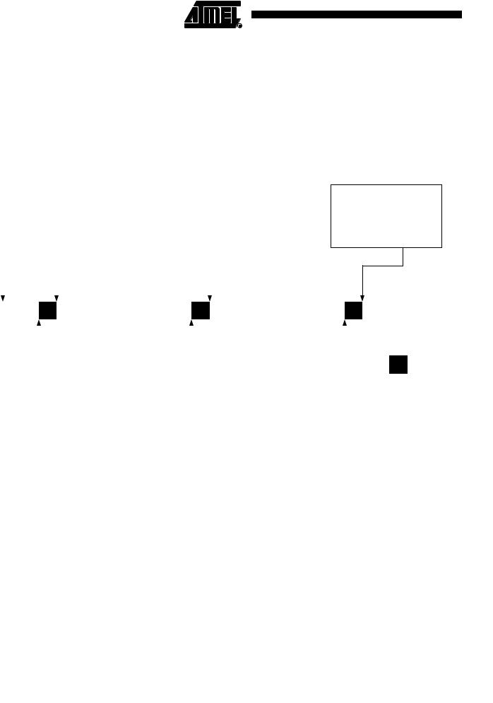
TWI Data Register – TWDR
Bit |
7 |
6 |
5 |
4 |
3 |
2 |
1 |
0 |
|
|
TWD7 |
TWD6 |
TWD5 |
TWD4 |
TWD3 |
TWD2 |
TWD1 |
TWD0 |
TWDR |
|
|
|
|
|
|
|
|
|
|
Read/Write |
R/W |
R/W |
R/W |
R/W |
R/W |
R/W |
R/W |
R/W |
|
Initial Value |
1 |
1 |
1 |
1 |
1 |
1 |
1 |
1 |
|
In Transmit mode, TWDR contains the next byte to be transmitted. In receive mode, the TWDR contains the last byte received. It is writable while the TWI is not in the process of shifting a byte. This occurs when the TWI interrupt flag (TWINT) is set by hardware. Note that the Data Register cannot be initialized by the user before the first interrupt occurs. The data in TWDR remains stable as long as TWINT is set. While data is shifted out, data on the bus is simultaneously shifted in. TWDR always contains the last byte present on the bus, except after a wake up from a sleep mode by the TWI interrupt. In this case, the contents of TWDR is undefined. In the case of a lost bus arbitration, no data is lost in the transition from Master to Slave. Handling of the ACK bit is controlled automatically by the TWI logic, the CPU cannot access the ACK bit directly.
• Bits 7..0 – TWD: TWI Data Register
These eight bits constitute the next data byte to be transmitted, or the latest data byte received on the Two-wire Serial Bus.
TWI (Slave) Address Register
– TWAR
Using the TWI
2467K–AVR–04/04
Bit |
7 |
6 |
5 |
4 |
3 |
2 |
1 |
0 |
|
|
TWA6 |
TWA5 |
TWA4 |
TWA3 |
TWA2 |
TWA1 |
TWA0 |
TWGCE |
TWAR |
|
|
|
|
|
|
|
|
|
|
Read/Write |
R/W |
R/W |
R/W |
R/W |
R/W |
R/W |
R/W |
R/W |
|
Initial Value |
1 |
1 |
1 |
1 |
1 |
1 |
1 |
0 |
|
The TWAR should be loaded with the 7-bit slave address (in the seven most significant bits of TWAR) to which the TWI will respond when programmed as a slave transmitter or receiver, and not needed in the master modes. In multimaster systems, TWAR must be set in masters which can be addressed as slaves by other masters.
The LSB of TWAR is used to enable recognition of the general call address ($00). There is an associated address comparator that looks for the slave address (or general call address if enabled) in the received serial address. If a match is found, an interrupt request is generated.
• Bits 7..1 – TWA: TWI (Slave) Address Register
These seven bits constitute the slave address of the TWI unit.
• Bit 0 – TWGCE: TWI General Call Recognition Enable Bit
If set, this bit enables the recognition of a General Call given over the Two-wire Serial Bus.
The AVR TWI is byte-oriented and interrupt based. Interrupts are issued after all bus events, like reception of a byte or transmission of a START condition. Because the TWI is interrupt-based, the application software is free to carry on other operations during a TWI byte transfer. Note that the TWI Interrupt Enable (TWIE) bit in TWCR together with the Global Interrupt Enable bit in SREG allow the application to decide whether or not assertion of the TWINT flag should generate an interrupt request. If the TWIE bit is cleared, the application must poll the TWINT flag in order to detect actions on the TWI bus.
209
When the TWINT flag is asserted, the TWI has finished an operation and awaits application response. In this case, the TWI Status Register (TWSR) contains a value indicating the current state of the TWI bus. The application software can then decide how the TWI should behave in the next TWI bus cycle by manipulating the TWCR and TWDR Registers.
Figure 95 is a simple example of how the application can interface to the TWI hardware. In this example, a master wishes to transmit a single data byte to a slave. This description is quite abstract, a more detailed explanation follows later in this section. A simple code example implementing the desired behavior is also presented.
Figure 95. Interfacing the Application to the TWI in a Typical Transmission
Application |
Action |
1. Application |
|
3. Check TWSR to see if START |
|
5. Check TWSR to see if SLA+W |
||||||
writes to TWCR |
|
was sent. Application loads |
|
was sent and ACK received. |
||||||||
|
|
|
|
|||||||||
|
|
to initiate |
|
SLA+W into TWDR, and loads |
|
Application loads data into TWDR, |
||||||
|
|
transmission of |
|
appropriate control signals into |
|
and loads appropriate control signals |
||||||
|
|
START |
|
TWCR, making sure that TWINT |
|
into TWCR, making sure that TWINT |
||||||
|
|
|
|
|
|
|
is written to one, and TWSTA is |
|
is written to one. |
|||
|
|
|
|
|
|
|
written to zero. |
|
|
|
|
|
|
|
|
|
|
|
|
|
|
|
|
|
|
|
|
|
|
|
|
|
|
|
|
|
|
|
7. Check TWSR to see if data was sent and ACK received. Application loads appropriate control signals to send STOP into TWCR, making sure that TWINT is written to one
TWI bus |
START |
|
SLA+W |
A |
|
Data |
A |
|
STOP |
|
|
|
|
|
|
|
|
|
|
|
|
|
|
|
|
|
|
|
|
|
|
|
|
Indicates |
|
|
|
|
|
|
|
|
|
|
|
|
|
|
|
|
2. TWINT set. |
|
4. TWINT set. |
|
6. TWINT set. |
|
|
|||||||
|
|
|
|
|
TWINT set |
|||||||||
TWI |
Status code indicates |
|
Status code indicates |
|
Status code indicates |
|
|
|||||||
|
|
|
|
|
||||||||||
START condition sent |
|
SLA+W sendt, ACK |
|
data sent, ACK received |
|
|
|
|||||||
Hardware |
|
|
|
|
|
|||||||||
|
|
|
|
received |
|
|
|
|
|
|
|
|||
Action |
|
|
|
|
|
|
|
|
|
|
|
|
|
|
1.The first step in a TWI transmission is to transmit a START condition. This is done by writing a specific value into TWCR, instructing the TWI hardware to transmit a START condition. Which value to write is described later on. However, it is important that the TWINT bit is set in the value written. Writing a one to TWINT clears the flag. The TWI will not start any operation as long as the TWINT bit in TWCR is set. Immediately after the application has cleared TWINT, the TWI will initiate transmission of the START condition.
2.When the START condition has been transmitted, the TWINT flag in TWCR is set, and TWSR is updated with a status code indicating that the START condition has successfully been sent.
3.The application software should now examine the value of TWSR, to make sure that the START condition was successfully transmitted. If TWSR indicates otherwise, the application software might take some special action, like calling an error routine. Assuming that the status code is as expected, the application must load SLA+W into TWDR. Remember that TWDR is used both for address and data. After TWDR has been loaded with the desired SLA+W, a specific value must be written to TWCR, instructing the TWI hardware to transmit the SLA+W present in TWDR. Which value to write is described later on. However, it is important that the TWINT bit is set in the value written. Writing a one to TWINT clears the flag. The TWI will not start any operation as long as the TWINT bit in
210 ATmega128 
2467K–AVR–04/04
 ATmega128
TWCR is set. Immediately after the application has cleared TWINT, the TWI will initiate transmission of the address packet.
4.When the address packet has been transmitted, the TWINT flag in TWCR is set, and TWSR is updated with a status code indicating that the address packet has successfully been sent. The status code will also reflect whether a slave acknowledged the packet or not.
5.The application software should now examine the value of TWSR, to make sure that the address packet was successfully transmitted, and that the value of the ACK bit was as expected. If TWSR indicates otherwise, the application software might take some special action, like calling an error routine. Assuming that the status code is as expected, the application must load a data packet into TWDR. Subsequently, a specific value must be written to TWCR, instructing the TWI hardware to transmit the data packet present in TWDR. Which value to write is described later on. However, it is important that the TWINT bit is set in the value written. Writing a one to TWINT clears the flag. The TWI will not start any operation as long as the TWINT bit in TWCR is set. Immediately after the application has cleared TWINT, the TWI will initiate transmission of the data packet.
6.When the data packet has been transmitted, the TWINT flag in TWCR is set, and TWSR is updated with a status code indicating that the data packet has successfully been sent. The status code will also reflect whether a slave acknowledged the packet or not.
7.The application software should now examine the value of TWSR, to make sure that the data packet was successfully transmitted, and that the value of the ACK bit was as expected. If TWSR indicates otherwise, the application software might take some special action, like calling an error routine. Assuming that the status code is as expected, the application must write a specific value to TWCR, instructing the TWI hardware to transmit a STOP condition. Which value to write is described later on. However, it is important that the TWINT bit is set in the value written. Writing a one to TWINT clears the flag. The TWI will not start any operation as long as the TWINT bit in TWCR is set. Immediately after the application has cleared TWINT, the TWI will initiate transmission of the STOP condition. Note that TWINT is NOT set after a STOP condition has been sent.
211
2467K–AVR–04/04

Even though this example is simple, it shows the principles involved in all TWI transmissions. These can be summarized as follows:
•When the TWI has finished an operation and expects application response, the TWINT flag is set. The SCL line is pulled low until TWINT is cleared.
•When the TWINT flag is set, the user must update all TWI Registers with the value relevant for the next TWI bus cycle. As an example, TWDR must be loaded with the value to be transmitted in the next bus cycle.
•After all TWI Register updates and other pending application software tasks have been completed, TWCR is written. When writing TWCR, the TWINT bit should be set. Writing a one to TWINT clears the flag. The TWI will then commence executing whatever operation was specified by the TWCR setting.
In the following an assembly and C implementation of the example is given. Note that the code below assumes that several definitions have been made for example by using include-files.
212 ATmega128
2467K–AVR–04/04

 ATmega128
|
Assembly Code Example |
C Example |
Comments |
||
|
|
|
|
|
|
1 |
|
ldi |
r16, |
TWCR = (1<<TWINT)|(1<<TWSTA)| |
|
|
|
(1<<TWINT)|(1<<TWSTA)| |
(1<<TWEN) |
Send START condition |
|
|
|
|
|
||
|
|
|
(1<<TWEN) |
|
|
|
|
|
|
|
|
|
|
out |
TWCR, r16 |
|
|
2 |
|
wait1: |
while (!(TWCR & (1<<TWINT))) |
|
|
|
|
in |
r16,TWCR |
; |
Wait for TWINT flag set. This indicates that the |
|
|
sbrs |
r16,TWINT |
|
START condition has been transmitted |
|
|
|
|
||
|
|
rjmp |
wait1 |
|
|
3 |
|
in |
r16,TWSR |
if ((TWSR & 0xF8) != START) |
Check value of TWI Status Register. Mask |
|
|
andi |
r16, 0xF8 |
ERROR(); |
|
|
|
prescaler bits. If status different from START |
|||
|
|
cpi |
r16, START |
|
|
|
|
|
go to ERROR |
||
|
|
|
|
|
|
|
|
brne |
ERROR |
|
|
|
|
ldi |
r16, SLA_W |
TWDR = SLA_W; |
|
|
|
out |
TWDR, r16 |
TWCR = (1<<TWINT) | |
Load SLA_W into TWDR Register. Clear |
|
|
ldi |
r16, (1<<TWINT) | |
(1<<TWEN); |
TWINT bit in TWCR to start transmission of |
|
|
(1<<TWEN) |
|
address |
|
|
|
|
|
||
|
|
out |
TWCR, r16 |
|
|
4 |
|
wait2: |
while (!(TWCR & (1<<TWINT))) |
Wait for TWINT flag set. This indicates that the |
|
|
|
in |
r16,TWCR |
; |
|
|
|
SLA+W has been transmitted, and |
|||
|
|
sbrs |
r16,TWINT |
|
|
|
|
|
ACK/NACK has been received. |
||
|
|
|
|
|
|
|
|
rjmp |
wait2 |
|
|
5 |
|
in |
r16,TWSR |
if ((TWSR & 0xF8) != |
Check value of TWI Status Register. Mask |
|
|
andi |
r16, 0xF8 |
MT_SLA_ACK) |
|
|
|
|
prescaler bits. If status different from |
||
|
|
cpi |
r16, MT_SLA_ACK |
ERROR(); |
|
|
|
MT_SLA_ACK go to ERROR |
|||
|
|
|
|||
|
|
|
|
|
|
|
|
brne |
ERROR |
|
|
|
|
ldi |
r16, DATA |
TWDR = DATA; |
|
|
|
out |
TWDR, r16 |
TWCR = (1<<TWINT) | |
Load DATA into TWDR Register. Clear TWINT |
|
|
ldi |
r16, (1<<TWINT) | |
(1<<TWEN); |
|
|
|
bit in TWCR to start transmission of data |
|||
|
|
|
|||
|
|
(1<<TWEN) |
|
||
|
|
|
|
||
|
|
out |
TWCR, r16 |
|
|
6 |
|
wait3: |
while (!(TWCR & (1<<TWINT))) |
Wait for TWINT flag set. This indicates that the |
|
|
|
in |
r16,TWCR |
; |
|
|
|
DATA has been transmitted, and ACK/NACK |
|||
|
|
sbrs |
r16,TWINT |
|
|
|
|
|
has been received. |
||
|
|
|
|
|
|
|
|
rjmp |
wait3 |
|
|
7 |
|
in |
r16,TWSR |
if ((TWSR & 0xF8) != |
Check value of TWI Status Register. Mask |
|
|
andi |
r16, 0xF8 |
MT_DATA_ACK) |
|
|
|
|
prescaler bits. If status different from |
||
|
|
cpi |
r16, MT_DATA_ACK |
ERROR(); |
|
|
|
MT_DATA_ACK go to ERROR |
|||
|
|
|
|||
|
|
|
|
|
|
|
|
brne |
ERROR |
|
|
|
|
ldi |
r16, |
TWCR = (1<<TWINT)|(1<<TWEN)| |
|
|
|
(1<<TWINT)|(1<<TWEN)| |
(1<<TWSTO); |
Transmit STOP condition |
|
|
|
|
|
||
|
|
|
(1<<TWSTO) |
|
|
|
|
|
|
|
|
|
|
out |
TWCR, r16 |
|
|
Note: |
For I/O registers located in extended I/O map, “IN”, “OUT”, “SBIS”, “SBIC”, “CBI”, and “SBI” instructions must be replaced with |
||||
|
|
instructions that allow access to extended I/O. Typically “LDS” and “STS” combined with “SBRS”, “SBRC”, “SBR”, and “CBR”. |
|||
213
2467K–AVR–04/04