

|
|
|
|
|
|
|
|
|
|
|
|
|
|
|
|
ATtiny13 |
|
|
|
|
|
|
|
|
|
|
|
|
|
|
|
|
|
||
Modes of Operation |
|
|
|
|
|
|
|
|
|
|
|
|
|
|
|||
The mode of operation, i.e., the behavior of the Timer/Counter and the Output Compare |
|||||||||||||||||
|
|
pins, is defined by the combination of the Waveform Generation mode (WGM02:0) and |
|||||||||||||||
|
|
Compare Output mode (COM0x1:0) bits. The Compare Output mode bits do not affect |
|||||||||||||||
|
|
the counting sequence, while the Waveform Generation mode bits do. The COM0x1:0 |
|||||||||||||||
|
|
bits control whether the PWM output generated should be inverted or not (inverted or |
|||||||||||||||
|
|
non-inverted PWM). For non-PWM modes the COM0x1:0 bits control whether the out- |
|||||||||||||||
|
|
put should be set, cleared, or toggled at a Compare Match (See “Compare Match |
|||||||||||||||
|
|
Output Unit” on page 58.). |
|||||||||||||||
|
|
For detailed timing information refer to Figure 32, Figure 33, Figure 34 and Figure 35 in |
|||||||||||||||
|
|
“Timer/Counter Timing Diagrams” on page 63. |
|||||||||||||||
Normal Mode |
The simplest mode of operation is the Normal mode (WGM02:0 = 0). In this mode the |
||||||||||||||||
|
|
counting direction is always up (incrementing), and no counter clear is performed. The |
|||||||||||||||
|
|
counter simply overruns when it passes its maximum 8-bit value (TOP = 0xFF) and then |
|||||||||||||||
|
|
restarts from the bottom (0x00). In normal operation the Timer/Counter Overflow Flag |
|||||||||||||||
|
|
(TOV0) will be set in the same timer clock cycle as the TCNT0 becomes zero. The |
|||||||||||||||
|
|
TOV0 Flag in this case behaves like a ninth bit, except that it is only set, not cleared. |
|||||||||||||||
|
|
However, combined with the timer overflow interrupt that automatically clears the TOV0 |
|||||||||||||||
|
|
Flag, the timer resolution can be increased by software. There are no special cases to |
|||||||||||||||
|
|
consider in the Normal mode, a new counter value can be written anytime. |
|||||||||||||||
|
|
The Output Compare Unit can be used to generate interrupts at some given time. Using |
|||||||||||||||
|
|
the Output Compare to generate waveforms in Normal mode is not recommended, |
|||||||||||||||
|
|
since this will occupy too much of the CPU time. |
|||||||||||||||
Clear Timer on Compare |
In Clear Timer on Compare or CTC mode (WGM02:0 = 2), the OCR0A Register is used |
||||||||||||||||
Match (CTC) Mode |
to manipulate the counter resolution. In CTC mode the counter is cleared to zero when |
||||||||||||||||
|
|
the counter value (TCNT0) matches the OCR0A. The OCR0A defines the top value for |
|||||||||||||||
|
|
the counter, hence also its resolution. This mode allows greater control of the Compare |
|||||||||||||||
|
|
Match output frequency. It also simplifies the operation of counting external events. |
|||||||||||||||
|
|
The timing diagram for the CTC mode is shown in Figure 29. The counter value |
|||||||||||||||
|
|
(TCNT0) increases until a Compare Match occurs between TCNT0 and OCR0A, and |
|||||||||||||||
|
|
then counter (TCNT0) is cleared. |
|||||||||||||||
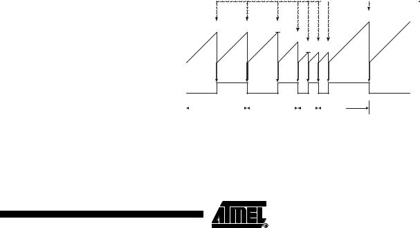
|
|
Figure 29. CTC Mode, Timing Diagram |
|||||||||||||||
|
|
|
|
|
|
|
|
|
|
|
|
|
|
|
|
|
|
|
|
|
|
|
|
|
|
|
|
|
|
|
|
|
OCnx Interrupt Flag Set |
|
|
|
|
|
|
|
|
|
|
|
|
|
|
|
|
|
|
|
|
|
|
|
|
|
|
|
|
|
|
|
|
|
|
|
|
|
|
|
|
|
|
|
|
|
|
|
|
|
|
|
|
|
|
|
|
|
|
|
|
|
|
|
|
|
|
|
|
|
|
|
|
|
|
|
|
|
|
|
|
|
|
|
|
|
|
|
|
|
|
|
|
TCNTn
OCn
(COMnx1:0 = 1)
(Toggle)
Period |
|
|
|
|
|
|
|
|
|
|
|
|
|
|
|
|
|
|
|
|
1 |
|
|
|
|
2 |
|
|
|
|
3 |
|
|
|
|
4 |
|
|
|
|
|
|
|
|
||||||||||||
|
|
|
|
|
|
|
|
|
|
|
|
|
|
|
|
|
|
|
An interrupt can be generated each time the counter value reaches the TOP value by using the OCF0A Flag. If the interrupt is enabled, the interrupt handler routine can be used for updating the TOP value. However, changing TOP to a value close to BOTTOM when the counter is running with none or a low prescaler value must be done with care since the CTC mode does not have the double buffering feature. If the new value written
59
2535A–AVR–06/03

to OCR0A is lower than the current value of TCNT0, the counter will miss the Compare Match. The counter will then have to count to its maximum value (0xFF) and wrap around starting at 0x00 before the Compare Match can occur.
For generating a waveform output in CTC mode, the OC0A output can be set to toggle its logical level on each Compare Match by setting the Compare Output mode bits to toggle mode (COM0A1:0 = 1). The OC0A value will not be visible on the port pin unless the data direction for the pin is set to output. The waveform generated will have a maxi-
mum frequency of fOC0 = fclk_I/O/2 when OCR0A is set to zero (0x00). The waveform frequency is defined by the following equation:
|
fO Cn x = |
fclk_I/O |
|
2--------N---------(--1-----+-----OC---------Rnx-----------) |
|
|
The N variable represents the prescale factor (1, 8, 64, 256, or 1024). |
|
|
As for the Normal mode of operation, the TOV0 Flag is set in the same timer clock cycle |
|
|
that the counter counts from MAX to 0x00. |
|
Fast PWM Mode |
The fast Pulse Width Modulation or fast PWM mode (WGM02:0 = 3 or 7) provides a high |
|
|
frequency PWM waveform generation option. The fast PWM differs from the other PWM |
|
|
option by its single-slope operation. The counter counts from BOTTOM to TOP then |
|
restarts from BOTTOM. TOP is defined as 0xFF when WGM2:0 = 3, and OCR0A when WGM2:0 = 7. In non-inverting Compare Output mode, the Output Compare (OC0x) is cleared on the Compare Match between TCNT0 and OCR0x, and set at BOTTOM. In inverting Compare Output mode, the output is set on Compare Match and cleared at BOTTOM. Due to the single-slope operation, the operating frequency of the fast PWM mode can be twice as high as the phase correct PWM mode that use dual-slope operation. This high frequency makes the fast PWM mode well suited for power regulation, rectification, and DAC applications. High frequency allows physically small sized external components (coils, capacitors), and therefore reduces total system cost.
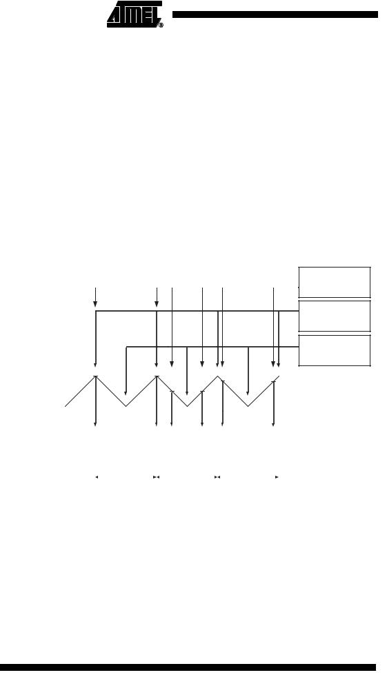
In fast PWM mode, the counter is incremented until the counter value matches the TOP value. The counter is then cleared at the following timer clock cycle. The timing diagram for the fast PWM mode is shown in Figure 30. The TCNT0 value is in the timing diagram shown as a histogram for illustrating the single-slope operation. The diagram includes non-inverted and inverted PWM outputs. The small horizontal line marks on the TCNT0 slopes represent Compare Matches between OCR0x and TCNT0.
60 ATtiny13
2535A–AVR–06/03
ATtiny13
Figure 30. Fast PWM Mode, Timing Diagram
OCRnx Interrupt Flag Set
OCRnx Update and
TOVn Interrupt Flag Set
TCNTn
OCn |
|
|
|
|
|
|
|
|
|
|
|
|
|
|
|
|
|
|
|
|
|
|
|
|
|
|
|
|
|
|
|
|
|
|
|
|
|
|
|
|
(COMnx1:0 = 2) |
|
|
|
|
|
|
|
|
|
|
|
|
|
|
|
|
|
|
|
|
|
|
|
|
|
|
|
|
|
|
|
|
|
|
|
|
|
|
|
|
|
|
|
|
OCn |
|
|
|
|
|
|
|
|
|
|
|
|
|
|
|
|
|
|
|
|
|
|
|
|
|
|
|
|
|
|
|
|
|
|
|
|
|
|
|
|
(COMnx1:0 = 3) |
|
Period |
|
|
|
|
|
|
|
|
|
|
|
|
|
|
|
|
|
|
|
|
|
|
|
|
|
|
|
|
|
|
|
|
|
|
|
|
|
|
|
|
|
|
|
|
|
|
|
|
|
|
|
|
|
|
|
|
|
|
|
|
|
|
|
|
|
|
|
|
|
|
|
|
|
|
|
|
|
|
|
|
|
|
|
||
|
|
1 |
|
|
|
|
2 |
|
|
|
|
3 |
|
|
|
|
|
4 |
|
|
|
|
|
5 |
|
|
|
|
6 |
|
|
|
|
|
7 |
|
|
|
|
|||
|
|
|
|
|
|
|
|
|
|
|
|
|
|
|
|
|
||||||||||||||||||||||||||
|
|
|
|
|
|
|
|
|
|
|
|
|
|
|
|
|
|
|
|
|
|
|
|
|
|
|
|
|
|
|
|
|
|
|
|
|
|
|
|
|
|
|
The Timer/Counter Overflow Flag (TOV0) is set each time the counter reaches TOP. If the interrupt is enabled, the interrupt handler routine can be used for updating the compare value.
In fast PWM mode, the compare unit allows generation of PWM waveforms on the OC0x pins. Setting the COM0x1:0 bits to two will produce a non-inverted PWM and an inverted PWM output can be generated by setting the COM0x1:0 to three: Setting the COM0A1:0 bits to one allowes the AC0A pin to toggle on Compare Matches if the WGM02 bit is set. This option is not available for the OC0B pin (See Table 28 on page 65). The actual OC0x value will only be visible on the port pin if the data direction for the port pin is set as output. The PWM waveform is generated by setting (or clearing) the OC0x Register at the Compare Match between OCR0x and TCNT0, and clearing (or setting) the OC0x Register at the timer clock cycle the counter is cleared (changes from TOP to BOTTOM).
The PWM frequency for the output can be calculated by the following equation:
fclk_I/O fO Cn xPW M = -----------------
N 256
The N variable represents the prescale factor (1, 8, 64, 256, or 1024).
The extreme values for the OCR0A Register represents special cases when generating a PWM waveform output in the fast PWM mode. If the OCR0A is set equal to BOTTOM, the output will be a narrow spike for each MAX+1 timer clock cycle. Setting the OCR0A equal to MAX will result in a constantly high or low output (depending on the polarity of the output set by the COM0A1:0 bits.)
A frequency (with 50% duty cycle) waveform output in fast PWM mode can be achieved by setting OC0x to toggle its logical level on each Compare Match (COM0x1:0 = 1). The waveform generated will have a maximum frequency of fOC0 = fclk_I/O/2 when OCR0A is set to zero. This feature is similar to the OC0A toggle in CTC mode, except the double buffer feature of the Output Compare unit is enabled in the fast PWM mode.
61
2535A–AVR–06/03
Phase Correct PWM Mode The phase correct PWM mode (WGM02:0 = 1 or 5) provides a high resolution phase correct PWM waveform generation option. The phase correct PWM mode is based on a dual-slope operation. The counter counts repeatedly from BOTTOM to TOP and then from TOP to BOTTOM. TOP is defined as 0xFF when WGM2:0 = 1, and OCR0A when WGM2:0 = 5. In non-inverting Compare Output mode, the Output Compare (OC0x) is cleared on the Compare Match between TCNT0 and OCR0x while upcounting, and set on the Compare Match while down-counting. In inverting Output Compare mode, the operation is inverted. The dual-slope operation has lower maximum operation frequency than single slope operation. However, due to the symmetric feature of the dual-slope PWM modes, these modes are preferred for motor control applications.
In phase correct PWM mode the counter is incremented until the counter value matches TOP. When the counter reaches TOP, it changes the count direction. The TCNT0 value will be equal to TOP for one timer clock cycle. The timing diagram for the phase correct PWM mode is shown on Figure 31. The TCNT0 value is in the timing diagram shown as a histogram for illustrating the dual-slope operation. The diagram includes non-inverted and inverted PWM outputs. The small horizontal line marks on the TCNT0 slopes represent Compare Matches between OCR0x and TCNT0.
Figure 31. Phase Correct PWM Mode, Timing Diagram
OCnx Interrupt Flag Set
OCRnx Update
TOVn Interrupt Flag Set
TCNTn
OCn |
|
|
|
|
|
|
|
|
|
|
|
|
|
|
|
|
|
|
|
|
(COMnx1:0 = 2) |
|
|
|
|
|
|
|
|
|
|
|
|
|
|
|
|
|
|
|
|
|
|
|
|
|
|
|
|
|
|
|
|
|
|
|
|
|
|
|
|
|
|
|
|
|
|
|
OCn |
|
|
|
|
|
|
|
|
|
|
|
|
|
|
|
|
|
|
|
(COMnx1:0 = 3) |
||
|
|
|
|
|
|
|
|
|
|
|
|
|
|
|
|
|
|
|
||||
|
|
|
|
|
|
|
|
|
|
|
|
|
|
|
|
|
|
|
|
|
|
|
Period |
|
|
|
|
|
|
|
|
|
|
|
|
|
|
|
|
|
|
|
|
||
|
|
|
|
|
|
|
|
|
|
|
|
|
|
|
|
|
|
|
|
|||
|
|
1 |
|
|
|
|
|
2 |
|
|
|
|
|
|
3 |
|
|
|
|
|||
|
|
|
|
|
|
|
|
|
|
|||||||||||||
|
|
|
|
|
|
|
|
|
|
|
|
|
|
|
|
|
|
|
|
|
|
|
The Timer/Counter Overflow Flag (TOV0) is set each time the counter reaches BOTTOM. The Interrupt Flag can be used to generate an interrupt each time the counter reaches the BOTTOM value.
In phase correct PWM mode, the compare unit allows generation of PWM waveforms on the OC0x pins. Setting the COM0x1:0 bits to two will produce a non-inverted PWM. An inverted PWM output can be generated by setting the COM0x1:0 to three: Setting the COM0A0 bits to one allows the OC0A pin to toggle on Compare Matches if the WGM02 bit is set. This option is not available for the OC0B pin (See Table 29 on page 66). The actual OC0x value will only be visible on the port pin if the data direction for the port pin is set as output. The PWM waveform is generated by clearing (or setting) the OC0x Register at the Compare Match between OCR0x and TCNT0 when the counter increments, and setting (or clearing) the OC0x Register at Compare Match between OCR0x
62 ATtiny13
2535A–AVR–06/03

Timer/Counter Timing
Diagrams
ATtiny13
and TCNT0 when the counter decrements. The PWM frequency for the output when using phase correct PWM can be calculated by the following equation:
fO Cnx PCP WM |
fclk_I/O |
= ----------------- |
|
|
N 510 |
The N variable represents the prescale factor (1, 8, 64, 256, or 1024).
The extreme values for the OCR0A Register represent special cases when generating a PWM waveform output in the phase correct PWM mode. If the OCR0A is set equal to BOTTOM, the output will be continuously low and if set equal to MAX the output will be continuously high for non-inverted PWM mode. For inverted PWM the output will have the opposite logic values.
At the very start of period 2 in Figure 31 OCn has a transition from high to low even though there is no Compare Match. The point of this transition is to guaratee symmetry around BOTTOM. There are two cases that give a transition without Compare Match.
•OCR0A changes its value from MAX, like in Figure 31. When the OCR0A value is MAX the OCn pin value is the same as the result of a down-counting Compare Match. To ensure symmetry around BOTTOM the OCn value at MAX must correspond to the result of an up-counting Compare Match.
•The timer starts counting from a value higher than the one in OCR0A, and for that reason misses the Compare Match and hence the OCn change that would have happened on the way up.
The Timer/Counter is a synchronous design and the timer clock (clkT0) is therefore shown as a clock enable signal in the following figures. The figures include information on when Interrupt Flags are set. Figure 32 contains timing data for basic Timer/Counter operation. The figure shows the count sequence close to the MAX value in all modes other than phase correct PWM mode.
Figure 32. Timer/Counter Timing Diagram, no Prescaling
clkI/O
clkTn
(clkI/O/1)
TCNTn |
MAX - 1 |
|
MAX |
|
BOTTOM |
|
BOTTOM + 1 |
|
|
|
|
|
|
|
|
TOVn
Figure 33 shows the same timing data, but with the prescaler enabled.
63
2535A–AVR–06/03
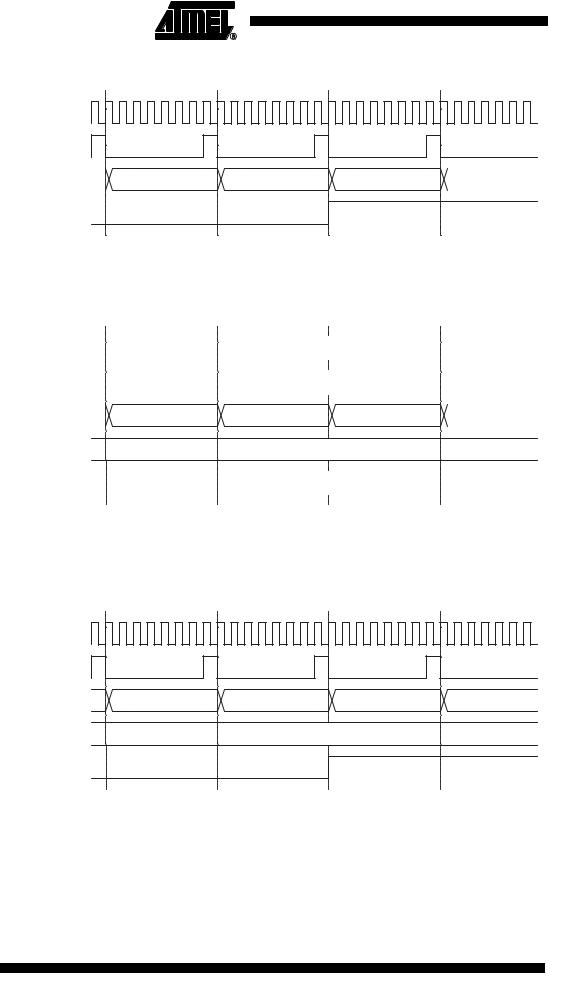
Figure 33. Timer/Counter Timing Diagram, with Prescaler (fclk_I/O/8)
clkI/O
clkTn
(clkI/O/8)
TCNTn |
|
|
MAX - 1 |
|
MAX |
|
BOTTOM |
|
|
BOTTOM + 1 |
|
|
|
|
|
|
|
|
|
|
|
TOVn
Figure 34 shows the setting of OCF0B in all modes and OCF0A in all modes except
CTC mode and PWM mode, where OCR0A is TOP.
Figure 34. Timer/Counter Timing Diagram, Setting of OCF0x, with Prescaler (fclk_I/O/8)
clkI/O |
|
|
|
|
|
|
|
|
|
|
|
|
|
|
|
|
|
|
|
|
|
|
|
|
|
|
|
|
|
|
|
|
|
|
|
|
|
|
|
|
|
|
|
|
|
|
|
|
|
|
|
|
|
|
|
|
|
|
|
|
|
|
|
|
clkTn |
|
|
|
|
|
|
|
|
|
|
|
|
|
|
|
|
|
|
|
|
|
|
|
|
|
|
|
|
|
|
|
|
|
|
|
|
|
|
|
|
|
|
|
|
|
|
|
|
|
|
|
|
|
|
|
|
|
|
|
|
|
|
|
|
|
|
|
|
|
|
|
|
|
|
|
|
|
|
|
|
|
|
|
|
|
|
|
|
|
|
|
|
|
|
|
|
|
|
|
|
|
|
|
|
|
|
|
|
|
|
|
|
|
|
|
|
|
|
|
|
|
|
|
|
|
|
|
|
|
|
|
|
|
|
|
|
|
|
|
|
|
|
|
|
|
|
|
|
|
|
|
|
|
|
|
|
|
|
|
|
|
|
|
|
|
|
|
|
|
|
|
|
|
|
|
|
|
|
|
|
|
|
|
|
|
|
|
|
|
|
|
|
|
|
(clkI/O/8) |
|
|
|
|
|
|
|
|
|
|
|
|
|
|
|
|
|
|
|
|
|
|
|
|
|
|
|
|
|
|
|
|
|
|
|
|
|
|
|
|
|
|
|
|
|
|
|
|
|
|
|
|
|
|
|
|
|
|
|
|
|
|
|
|
TCNTn |
|
|
|
|
|
|
|
|
|
|
|
|
|
|
|
|
|
|
|
|
|
|
|
|
|
|
|
|
|
|
|
|
|
|
|
|||||||||||||||||||||||||||||
|
|
|
|
|
|
|
|
OCRnx - 1 |
|
|
|
|
|
|
|
|
|
|
OCRnx |
|
|
|
|
|
|
|
|
OCRnx + 1 |
|
|
|
|
|
|
|
|
OCRnx + 2 |
|
|
|||||||||||||||||||||||||
OCRnx |
|
|
|
|
|
|
|
|
|
|
|
|
|
|
|
|
|
|
|
|
|
|
|
|
|
|
|
|
|
|
|
|
|
|
|
|
|
|
|
|
|
|
|
|
|
|
|
|
|
|
|
|
|
|
|
|
|
|||||||
|
|
|
|
|
|
|
|
|
|
|
|
|
|
|
|
|
|
|
|
|
|
|
|
|
|
|
|
|
|
|
|
|
|
|
|
|
|
|
|
|
|
|
|
|
|
|
|
|
|
|
|
|
|
|
|
|
|
|
|
|
|
|
|
|
|
|
|
|
|
|
|
|
|
|
|
|
|
|
|
|
|
|
|
|
|
|
|
|
|
|
|
|
|
OCRnx Value |
|
|
|
|
|
|
|
|
|
|
|
|
|
|
|
|
|
|
|
|
|
|
|
|
|
|
|||||||||
OCFnx |
|
|
|
|
|
|
|
|
|
|
|
|
|
|
|
|
|
|
|
|
|
|
|
|
|
|
|
|
|
|
|
|
|
|
|
|
|
|
|
|
|
|
|
|
|
|
|
|
|
|
|
|
|
|
|
|
|
|
|
|
|
|
|
|
|
|
|
|
|
|
|
|
|
|
|
|
|
|
|
|
|
|
|
|
|
|
|
|
|
|
|
|
|
|
|
|
|
|
|
|
|
|
|
|
|
|
|
|
|
|
|
|
|
|
|
|
|
|
|
|
|
|
|
|
|
|
|
|
|
|
|
|
|
|
|
|
|
|
|
|
|
|
|
|
|
|
|
|
|
|
|
|
|
|
|
|
|
|
|
|
|
|
|
|
|
|
|
|
|
|
|
|
|
|
|
|
|
|
|
|
|
|
|
|
|
|
|
|
|
|
|
|
|
|
|
|
|
|
|
|
|
|
|
|
|
|
|
|
|
|
|
|
|
|
|
|
|
|
|
|
|
|
|
|
|
|
|
|
|
|
|
|
|
|
|
|
|
|
|
|
|
|
|
|
|
|
|
|
|
|
|
|
|
|
|
|
|
|
|
Figure 35 shows the setting of OCF0A and the clearing of TCNT0 in CTC mode and fast
PWM mode where OCR0A is TOP.
Figure 35. Timer/Counter Timing Diagram, Clear Timer on Compare Match mode, with
Prescaler (fclk_I/O/8)
clkI/O |
|
|
|
|
|
clkTn |
|
|
|
|
|
(clkI/O/8) |
|
|
|
|
|
TCNTn |
TOP - 1 |
TOP |
BOTTOM |
BOTTOM + 1 |
|
(CTC) |
|||||
|
|
|
|
||
OCRnx |
|
|
TOP |
|
|
OCFnx |
|
|
|
|
64 ATtiny13
2535A–AVR–06/03

8-bit Timer/Counter
Register Description
Timer/Counter Control
Register A – TCCR0A
ATtiny13
Bit |
7 |
6 |
5 |
4 |
3 |
2 |
1 |
0 |
|
|
COM0A1 |
COM0A0 |
COM0B1 |
COM0B0 |
– |
– |
WGM01 |
WGM00 |
TCCR0A |
|
|
|
|
|
|
|
|
|
|
Read/Write |
R/W |
R/W |
R/W |
R/W |
R |
R |
R/W |
R/W |
|
Initial Value |
0 |
0 |
0 |
0 |
0 |
0 |
0 |
0 |
|
• Bits 7:6 – COM01A:0: Compare Match Output A Mode
These bits control the Output Compare pin (OC0A) behavior. If one or both of the COM0A1:0 bits are set, the OC0A output overrides the normal port functionality of the I/O pin it is connected to. However, note that the Data Direction Register (DDR) bit corresponding to the OC0A pin must be set in order to enable the output driver.
When OC0A is connected to the pin, the function of the COM0A1:0 bits depends on the WGM02:0 bit setting. Table 27 shows the COM0A1:0 bit functionality when the WGM02:0 bits are set to a normal or CTC mode (non-PWM).
Table 27. Compare Output Mode, non-PWM Mode
COM01 |
COM00 |
Description |
|
|
|
0 |
0 |
Normal port operation, OC0A disconnected. |
|
|
|
0 |
1 |
Toggle OC0A on Compare Match |
|
|
|
1 |
0 |
Clear OC0A on Compare Match |
|
|
|
1 |
1 |
Set OC0A on Compare Match |
|
|
|
Table 28 shows the COM0A1:0 bit functionality when the WGM01:0 bits are set to fast PWM mode.
Table 28. Compare Output Mode, Fast PWM Mode(1)
COM01 |
COM00 |
Description |
|
|
|
0 |
0 |
Normal port operation, OC0A disconnected. |
|
|
|
0 |
1 |
WGM02 = 0: Normal Port Operation, OC0A Disconnected. |
|
|
WGM02 = 1: Toggle OC0A on Compare Match. |
|
|
|
1 |
0 |
Clear OC0A on Compare Match, set OC0A at TOP |
|
|
|
1 |
1 |
Set OC0A on Compare Match, clear OC0A at TOP |
|
|
|
Note: 1. A special case occurs when OCR0A equals TOP and COM0A1 is set. In this case, the Compare Match is ignored, but the set or clear is done at TOP. See “Fast PWM Mode” on page 60 for more details.
65
2535A–AVR–06/03

Table 29 shows the COM0A1:0 bit functionality when the WGM02:0 bits are set to phase correct PWM mode.
Table 29. Compare Output Mode, Phase Correct PWM Mode(1)
COM0A1 |
COM0A0 |
Description |
|
|
|
0 |
0 |
Normal port operation, OC0A disconnected. |
|
|
|
0 |
1 |
WGM02 = 0: Normal Port Operation, OC0A Disconnected. |
|
|
WGM02 = 1: Toggle OC0A on Compare Match. |
|
|
|
1 |
0 |
Clear OC0A on Compare Match when up-counting. Set OC0A on |
|
|
Compare Match when down-counting. |
|
|
|
1 |
1 |
Set OC0A on Compare Match when up-counting. Clear OC0A on |
|
|
Compare Match when down-counting. |
|
|
|
Note: 1. A special case occurs when OCR0A equals TOP and COM0A1 is set. In this case, the Compare Match is ignored, but the set or clear is done at TOP. See “Phase Correct PWM Mode” on page 62 for more details.
• Bits 5:4 – COM0B1:0: Compare Match Output B Mode
These bits control the Output Compare pin (OC0B) behavior. If one or both of the COM0B1:0 bits are set, the OC0B output overrides the normal port functionality of the I/O pin it is connected to. However, note that the Data Direction Register (DDR) bit corresponding to the OC0B pin must be set in order to enable the output driver.
When OC0B is connected to the pin, the function of the COM0B1:0 bits depends on the
WGM02:0 bit setting. Table 27 shows the COM0A1:0 bit functionality when the
WGM02:0 bits are set to a normal or CTC mode (non-PWM).
Table 30. Compare Output Mode, non-PWM Mode
COM01 |
COM00 |
Description |
|
|
|
0 |
0 |
Normal port operation, OC0B disconnected. |
|
|
|
0 |
1 |
Toggle OC0B on Compare Match |
|
|
|
1 |
0 |
Clear OC0B on Compare Match |
|
|
|
1 |
1 |
Set OC0B on Compare Match |
|
|
|
Table 28 shows the COM0B1:0 bit functionality when the WGM02:0 bits are set to fast
PWM mode.
Table 31. Compare Output Mode, Fast PWM Mode(1)
COM01 |
COM00 |
Description |
|
|
|
0 |
0 |
Normal port operation, OC0B disconnected. |
|
|
|
0 |
1 |
Reserved |
|
|
|
1 |
0 |
Clear OC0B on Compare Match, set OC0B at TOP |
|
|
|
1 |
1 |
Set OC0B on Compare Match, clear OC0B at TOP |
|
|
|
Note: 1. A special case occurs when OCR0B equals TOP and COM0B1 is set. In this case, the Compare Match is ignored, but the set or clear is done at TOP. See “Fast PWM Mode” on page 60 for more details.
66 ATtiny13
2535A–AVR–06/03

 ATtiny13
Table 29 shows the COM0B1:0 bit functionality when the WGM02:0 bits are set to phase correct PWM mode.
Table 32. Compare Output Mode, Phase Correct PWM Mode(1)
COM0A1 |
COM0A0 |
Description |
|
|
|
0 |
0 |
Normal port operation, OC0B disconnected. |
|
|
|
0 |
1 |
Reserved |
|
|
|
1 |
0 |
Clear OC0B on Compare Match when up-counting. Set OC0B on |
|
|
Compare Match when down-counting. |
|
|
|
1 |
1 |
Set OC0B on Compare Match when up-counting. Clear OC0B on |
|
|
Compare Match when down-counting. |
|
|
|
Note: 1. A special case occurs when OCR0B equals TOP and COM0B1 is set. In this case, the Compare Match is ignored, but the set or clear is done at TOP. See “Phase Correct PWM Mode” on page 62 for more details.
• Bits 3, 2 – Res: Reserved Bits
These bits are reserved bits in the ATtiny13 and will always read as zero.
• Bits 1:0 – WGM01:0: Waveform Generation Mode
Combined with the WGM02 bit found in the TCCR0B Register, these bits control the counting sequence of the counter, the source for maximum (TOP) counter value, and what type of waveform generation to be used, see Table 33. Modes of operation supported by the Timer/Counter unit are: Normal mode (counter), Clear Timer on Compare Match (CTC) mode, and two types of Pulse Width Modulation (PWM) modes (see “Modes of Operation” on page 59).
Table 33. Waveform Generation Mode Bit Description
|
|
|
|
|
|
Timer/Counter |
|
|
|
|
|
|
|
|
|
Mode of |
|
Update of |
TOV Flag |
Mode |
WGM2 |
WGM1 |
|
WGM0 |
Operation |
TOP |
OCRx at |
Set on(1)(2) |
|
0 |
|
0 |
0 |
|
0 |
Normal |
0xFF |
Immediate |
MAX |
|
|
|
|
|
|
|
|
|
|
1 |
|
0 |
0 |
|
1 |
PWM, Phase |
0xFF |
TOP |
BOTTOM |
|
|
|
|
|
|
Correct |
|
|
|
|
|
|
|
|
|
|
|
|
|
2 |
|
0 |
1 |
|
0 |
CTC |
OCRA |
Immediate |
MAX |
|
|
|
|
|
|
|
|
|
|
3 |
|
0 |
1 |
|
1 |
Fast PWM |
0xFF |
TOP |
MAX |
|
|
|
|
|
|
|
|
|
|
4 |
|
1 |
0 |
|
0 |
Reserved |
– |
– |
– |
|
|
|
|
|
|
|
|
|
|
5 |
|
1 |
0 |
|
1 |
PWM, Phase |
OCRA |
TOP |
BOTTOM |
|
|
|
|
|
|
Correct |
|
|
|
|
|
|
|
|
|
|
|
|
|
6 |
|
1 |
1 |
|
0 |
Reserved |
– |
– |
– |
|
|
|
|
|
|
|
|
|
|
7 |
|
1 |
1 |
|
1 |
Fast PWM |
OCRA |
TOP |
TOP |
|
|
|
|
|
|
|
|
|
|
Notes: |
1. |
MAX |
= 0xFF |
|
|
|
|
|
|
|
2. |
BOTTOM = 0x00 |
|
|
|
|
|
||
67
2535A–AVR–06/03

Timer/Counter Control
Register B – TCCR0B
68 ATtiny13
|
|
|
|
|
|
|
|
|
|
|
|
|
|
|
|
|
|
|
|
|
|
|
|
|
|
Bit |
7 |
6 |
5 |
4 |
3 |
2 |
1 |
0 |
|
|||
|
|
|
|
|
|
|
|
|
|
|
|
|
|
FOC0A |
FOC0B |
|
|
– |
|
– |
WGM02 |
CS02 |
CS01 |
CS00 |
TCCR0B |
|
|
|
|
|
|
|
|
|
|
|
|
|
Read/Write |
W |
W |
|
|
R |
|
R |
R |
R |
R/W |
R/W |
|
Initial Value |
0 |
0 |
0 |
0 |
0 |
0 |
0 |
0 |
|
|||
• Bit 7 – FOC0A: Force Output Compare A
The FOC0A bit is only active when the WGM bits specify a non-PWM mode.
However, for ensuring compatibility with future devices, this bit must be set to zero when TCCR0B is written when operating in PWM mode. When writing a logical one to the FOC0A bit, an immediate Compare Match is forced on the Waveform Generation unit. The OC0A output is changed according to its COM0A1:0 bits setting. Note that the FOC0A bit is implemented as a strobe. Therefore it is the value present in the COM0A1:0 bits that determines the effect of the forced compare.
A FOC0A strobe will not generate any interrupt, nor will it clear the timer in CTC mode using OCR0A as TOP.
The FOC0A bit is always read as zero.
• Bit 6 – FOC0B: Force Output Compare B
The FOC0B bit is only active when the WGM bits specify a non-PWM mode.
However, for ensuring compatibility with future devices, this bit must be set to zero when TCCR0B is written when operating in PWM mode. When writing a logical one to the FOC0B bit, an immediate Compare Match is forced on the Waveform Generation unit. The OC0B output is changed according to its COM0B1:0 bits setting. Note that the FOC0B bit is implemented as a strobe. Therefore it is the value present in the COM0B1:0 bits that determines the effect of the forced compare.
A FOC0B strobe will not generate any interrupt, nor will it clear the timer in CTC mode using OCR0B as TOP.
The FOC0B bit is always read as zero.
• Bits 5:4 – Res: Reserved Bits
These bits are reserved bits in the ATtiny13 and will always read as zero.
• Bit 3 – WGM02: Waveform Generation Mode
See the description in the “Timer/Counter Control Register A – TCCR0A” on page 65.
• Bits 2:0 – CS02:0: Clock Select
The three Clock Select bits select the clock source to be used by the Timer/Counter.
Table 34. Clock Select Bit Description
|
CS02 |
CS01 |
CS00 |
Description |
|
|
|
|
|
|
|
|
0 |
0 |
0 |
No clock source (Timer/Counter stopped) |
|
|
|
|
|
|
|
|
0 |
0 |
1 |
clkI/O/(No prescaling) |
|
|
0 |
1 |
0 |
clkI/O/8 (From prescaler) |
|
|
0 |
1 |
1 |
clkI/O/64 (From prescaler) |
|
|
1 |
0 |
0 |
clkI/O/256 (From prescaler) |
|
|
|
|
|
|
|
|
|
|
|
|
|
2535A–AVR–06/03

 ATtiny13
Timer/Counter Register –
TCNT0
Table 34. |
Clock Select Bit Description (Continued) |
|||
CS02 |
|
CS01 |
CS00 |
Description |
|
|
|
|
|
1 |
|
0 |
1 |
clkI/O/1024 (From prescaler) |
1 |
|
1 |
0 |
External clock source on T0 pin. Clock on falling edge. |
|
|
|
|
|
1 |
|
1 |
1 |
External clock source on T0 pin. Clock on rising edge. |
|
|
|
|
|
If external pin modes are used for the Timer/Counter0, transitions on the T0 pin will clock the counter even if the pin is configured as an output. This feature allows software control of the counting.
Bit |
7 |
6 |
5 |
4 |
3 |
2 |
1 |
0 |
|
|
|
|
|
TCNT0[7:0] |
|
|
|
TCNT0 |
|
|
|
|
|
|
|
|
|
|
|
Read/Write |
R/W |
R/W |
R/W |
R/W |
R/W |
R/W |
R/W |
R/W |
|
Initial Value |
0 |
0 |
0 |
0 |
0 |
0 |
0 |
0 |
|
The Timer/Counter Register gives direct access, both for read and write operations, to the Timer/Counter unit 8-bit counter. Writing to the TCNT0 Register blocks (removes) the Compare Match on the following timer clock. Modifying the counter (TCNT0) while the counter is running, introduces a risk of missing a Compare Match between TCNT0 and the OCR0x Registers.
Output Compare Register A –
OCR0A
Bit |
7 |
6 |
5 |
4 |
3 |
2 |
1 |
0 |
|
|
|
|
|
OCR0A[7:0] |
|
|
|
OCR0A |
|
|
|
|
|
|
|
|
|
|
|
Read/Write |
R/W |
R/W |
R/W |
R/W |
R/W |
R/W |
R/W |
R/W |
|
Initial Value |
0 |
0 |
0 |
0 |
0 |
0 |
0 |
0 |
|
The Output Compare Register A contains an 8-bit value that is continuously compared with the counter value (TCNT0). A match can be used to generate an Output Compare interrupt, or to generate a waveform output on the OC0A pin.
Output Compare Register B –
OCR0B
Bit |
7 |
6 |
5 |
4 |
3 |
2 |
1 |
0 |
|
|
|
|
|
OCR0B[7:0] |
|
|
|
OCR0B |
|
|
|
|
|
|
|
|
|
|
|
Read/Write |
R/W |
R/W |
R/W |
R/W |
R/W |
R/W |
R/W |
R/W |
|
Initial Value |
0 |
0 |
0 |
0 |
0 |
0 |
0 |
0 |
|
The Output Compare Register B contains an 8-bit value that is continuously compared with the counter value (TCNT0). A match can be used to generate an Output Compare interrupt, or to generate a waveform output on the OC0B pin.
Timer/Counter Interrupt Mask
Register – TIMSK0
Bit |
7 |
6 |
5 |
4 |
3 |
2 |
1 |
0 |
|
|
– |
– |
– |
– |
OCIE0B |
OCIE0A |
TOIE0 |
– |
TIMSK0 |
|
|
|
|
|
|
|
|
|
|
Read/Write |
R |
R |
R |
R |
R/W |
R/W |
R/W |
R |
|
Initial Value |
0 |
0 |
0 |
0 |
0 |
0 |
0 |
0 |
|
• Bits 7..4, 0 – Res: Reserved Bits
These bits are reserved bits in the ATtiny13 and will always read as zero.
• Bit 3 – OCIE0B: Timer/Counter Output Compare Match B Interrupt Enable
When the OCIE0B bit is written to one, and the I-bit in the Status Register is set, the Timer/Counter Compare Match B interrupt is enabled. The corresponding interrupt is
69
2535A–AVR–06/03

Timer/Counter 0 Interrupt Flag
Register – TIFR0
executed if a Compare Match in Timer/Counter occurs, i.e., when the OCF0B bit is set in the Timer/Counter Interrupt Flag Register – TIFR0.
• Bit 2 – OCIE0A: Timer/Counter0 Output Compare Match A Interrupt Enable
When the OCIE0A bit is written to one, and the I-bit in the Status Register is set, the Timer/Counter0 Compare Match A interrupt is enabled. The corresponding interrupt is executed if a Compare Match in Timer/Counter0 occurs, i.e., when the OCF0A bit is set in the Timer/Counter 0 Interrupt Flag Register – TIFR0.
• Bit 1 – TOIE0: Timer/Counter0 Overflow Interrupt Enable
When the TOIE0 bit is written to one, and the I-bit in the Status Register is set, the Timer/Counter0 Overflow interrupt is enabled. The corresponding interrupt is executed if an overflow in Timer/Counter0 occurs, i.e., when the TOV0 bit is set in the Timer/Counter 0 Interrupt Flag Register – TIFR0.
Bit |
7 |
6 |
5 |
4 |
3 |
2 |
1 |
0 |
|
|
– |
– |
– |
– |
OCF0B |
OCF0A |
TOV0 |
– |
TIFR0 |
|
|
|
|
|
|
|
|
|
|
Read/Write |
R |
R |
R |
R |
R/W |
R/W |
R/W |
R |
|
Initial Value |
0 |
0 |
0 |
0 |
0 |
0 |
0 |
0 |
|
• Bits 7..4, 0 – Res: Reserved Bits
These bits are reserved bits in the ATtiny13 and will always read as zero.
• Bit 3 – OCF0B: Output Compare Flag 0 B
The OCF0B bit is set when a Compare Match occurs between the Timer/Counter and the data in OCR0B – Output Compare Register0 B. OCF0B is cleared by hardware when executing the corresponding interrupt handling vector. Alternatively, OCF0B is cleared by writing a logic one to the flag. When the I-bit in SREG, OCIE0B (Timer/Counter Compare B Match Interrupt Enable), and OCF0B are set, the Timer/Counter Compare Match Interrupt is executed.
• Bit 2 – OCF0A: Output Compare Flag 0 A
The OCF0A bit is set when a Compare Match occurs between the Timer/Counter0 and the data in OCR0A – Output Compare Register0. OCF0A is cleared by hardware when executing the corresponding interrupt handling vector. Alternatively, OCF0A is cleared by writing a logic one to the flag. When the I-bit in SREG, OCIE0A (Timer/Counter0 Compare Match Interrupt Enable), and OCF0A are set, the Timer/Counter0 Compare Match Interrupt is executed.
• Bit 1 – TOV0: Timer/Counter0 Overflow Flag
The bit TOV0 is set when an overflow occurs in Timer/Counter0. TOV0 is cleared by hardware when executing the corresponding interrupt handling vector. Alternatively, TOV0 is cleared by writing a logic one to the flag. When the SREG I-bit, TOIE0 (Timer/Counter0 Overflow Interrupt Enable), and TOV0 are set, the Timer/Counter0 Overflow interrupt is executed.
The setting of this flag is dependent of the WGM02:0 bit setting. Refer to Table 33, “Waveform Generation Mode Bit Description” on page 67.
70 ATtiny13
2535A–AVR–06/03