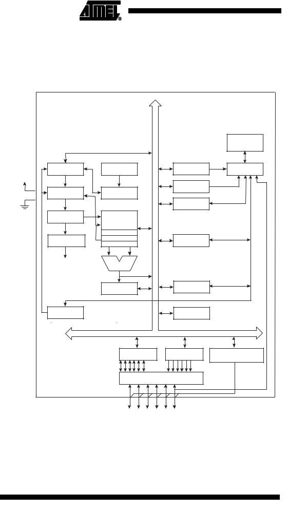
- •Features
- •Pin Configurations
- •Disclaimer
- •Overview
- •Block Diagram
- •Pin Descriptions
- •Port B (PB5..PB0)
- •RESET
- •AVR CPU Core
- •Introduction
- •Architectural Overview
- •Status Register
- •Stack Pointer
- •Interrupt Response Time
- •SRAM Data Memory
- •Data Memory Access Times
- •EEPROM Data Memory
- •EEPROM Read/Write Access
- •Atomic Byte Programming
- •Split Byte Programming
- •Erase
- •Write
- •I/O Memory
- •Clock Systems and their Distribution
- •CPU Clock – clkCPU
- •I/O Clock – clkI/O
- •Flash Clock – clkFLASH
- •ADC Clock – clkADC
- •Clock Sources
- •Default Clock Source
- •External Clock
- •System Clock Prescaler
- •Switching Time
- •Idle Mode
- •Power-down Mode
- •Analog to Digital Converter
- •Analog Comparator
- •Brown-out Detector
- •Internal Voltage Reference
- •Watchdog Timer
- •Port Pins
- •Resetting the AVR
- •Reset Sources
- •Power-on Reset
- •External Reset
- •Brown-out Detection
- •Watchdog Reset
- •Watchdog Timer
- •Timed Sequences for Changing the Configuration of the Watchdog Timer
- •Safety Level 1
- •Safety Level 2
- •Interrupts
- •I/O Ports
- •Introduction
- •Configuring the Pin
- •Toggling the Pin
- •Reading the Pin Value
- •Unconnected Pins
- •Alternate Port Functions
- •Alternate Functions of Port B
- •Register Description for I/O-Ports
- •Port B Data Register – PORTB
- •External Interrupts
- •8-bit Timer/Counter0 with PWM
- •Overview
- •Registers
- •Definitions
- •Counter Unit
- •Output Compare Unit
- •Force Output Compare
- •Modes of Operation
- •Normal Mode
- •Fast PWM Mode
- •Phase Correct PWM Mode
- •Prescaler Reset
- •External Clock Source
- •Analog Comparator
- •Analog Comparator Multiplexed Input
- •Features
- •Operation
- •Starting a Conversion
- •Changing Channel or Reference Selection
- •ADC Input Channels
- •ADC Voltage Reference
- •ADC Noise Canceler
- •Analog Input Circuitry
- •ADC Accuracy Definitions
- •ADC Conversion Result
- •ADLAR = 0
- •ADLAR = 1
- •debugWIRE On-chip Debug System
- •Features
- •Overview
- •Physical Interface
- •Software Break Points
- •Limitations of debugWIRE
- •debugWIRE Related Register in I/O Memory
- •debugWire Data Register – DWDR
- •Performing a Page Write
- •Reading the Fuse and Lock Bits from Software
- •Preventing Flash Corruption
- •Fuse Bytes
- •Latching of Fuses
- •Signature Bytes
- •Calibration Byte
- •Page Size
- •Serial Downloading
- •Data Polling Flash
- •Data Polling EEPROM
- •Chip Erase
- •Programming the Flash
- •Programming the EEPROM
- •Reading the Flash
- •Reading the EEPROM
- •Power-off sequence
- •Electrical Characteristics
- •Absolute Maximum Ratings*
- •External Clock Drive Waveforms
- •External Clock Drive
- •ADC Characteristics – Preliminary Data
- •Active Supply Current
- •Idle Supply Current
- •Power-down Supply Current
- •Pin Pull-up
- •Register Summary
- •Instruction Set Summary
- •Ordering Information
- •Packaging Information
- •Erratas
- •Table of Contents

Overview
The ATtiny13 is a low-power CMOS 8-bit microcontroller based on the AVR enhanced RISC architecture. By executing powerful instructions in a single clock cycle, the ATtiny13 achieves throughputs approaching 1 MIPS per MHz allowing the system designer to optimize power consumption versus processing speed.
Block Diagram |
Figure 2. Block Diagram |
8-BIT DATABUS
|
|
|
|
|
CALIBRATED |
|
|
|
|
|
INTERNAL |
|
|
|
|
|
OSCILLATOR |
|
|
PROGRAM |
STACK |
WATCHDOG |
TIMING AND |
|
|
COUNTER |
POINTER |
TIMER |
CONTROL |
|
VCC |
|
|
|
|
|
|
|
|
MCU CONTROL |
|
|
|
PROGRAM |
SRAM |
REGISTER |
|
|
|
|
|
||
|
|
FLASH |
|
|
|
|
|
|
|
|
|
|
|
|
|
MCU STATUS |
|
|
|
|
|
REGISTER |
|
|
GND |
INSTRUCTION |
GENERAL |
|
|
|
|
REGISTER |
PURPOSE |
|
|
|
|
|
REGISTERS |
|
|
|
|
|
X |
|
|
|
|
INSTRUCTION |
Y |
TIMER/ |
|
|
|
DECODER |
Z |
COUNTER0 |
|
|
|
CONTROL |
ALU |
|
|
|
|
LINES |
|
|
|
|
|
|
|
|
|
|
|
|
STATUS |
INTERRUPT |
|
|
|
|
UNIT |
|
|
|
|
|
REGISTER |
|
|
|
|
|
|
|
|
|
|
PROGRAMMING |
|
DATA |
|
|
|
LOGIC |
|
EEPROM |
|
|
|
ANALOG COMPARATOR |
DATA REGISTER |
DATA DIR. |
ADC / |
|
|
|
PORT B |
REG.PORT B |
ANALOG COMPARATOR |
|
|
|
PORT B DRIVERS |
|
|
|
|
|
|
|
RESET |
|
|
|
PB0-PB5 |
|
|
2 |
ATtiny13 |
|
|
|
|
|
|
|
|
|
2535A–AVR–06/03 |