

Watchdog Timer
Watchdog Timer Control
Register – WDTCR
ATtiny13
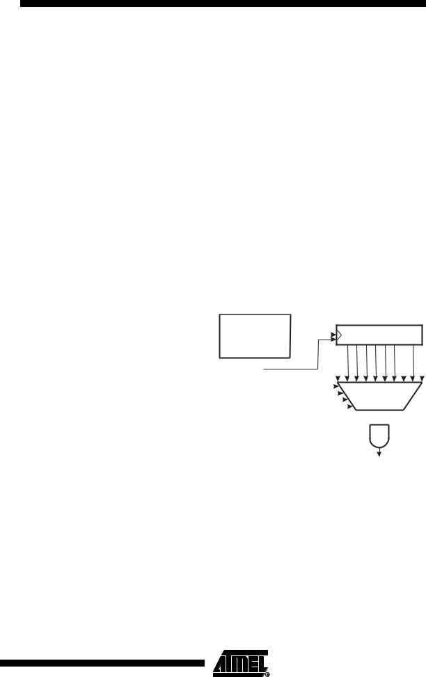
The Watchdog Timer is clocked from an On-chip Oscillator which runs at 128 kHz. By controlling the Watchdog Timer prescaler, the Watchdog Reset interval can be adjusted as shown in Table 18 on page 37. The WDR – Watchdog Reset – instruction resets the Watchdog Timer. The Watchdog Timer is also reset when it is disabled and when a Chip Reset occurs. Ten different clock cycle periods can be selected to determine the reset period. If the reset period expires without another Watchdog Reset, the ATtiny13 resets and executes from the Reset Vector. For timing details on the Watchdog Reset, refer to Table 18 on page 37.
The Wathdog Timer can also be configured to generate an interrupt instead of a reset. This can be very helpful when using the Watchdog to wake-up from Power-down.
To prevent unintentional disabling of the Watchdog or unintentional change of time-out period, two different safety levels are selected by the fuse WDTON as shown in Table 16. Refer to “Timed Sequences for Changing the Configuration of the Watchdog Timer” on page 39 for details.
Table 16. WDT Configuration as a Function of the Fuse Settings of WDTON
|
Safety |
WDT Initial |
How to Disable the |
How to Change |
WDTON |
Level |
State |
WDT |
Time-out |
|
|
|
|
|
Unprogrammed |
1 |
Disabled |
Timed sequence |
No limitations |
|
|
|
|
|
Programmed |
2 |
Enabled |
Always enabled |
Timed sequence |
|
|
|
|
|
Figure 19. Watchdog Timer
128 kHz |
|
|
|
|
|
|
|
WATCHDOG |
|
|
|
|
|
|||
OSCILLATOR |
|
|
|
|
|
|
|
PRESCALER |
|
|
|
|
|
|||
|
|
|
|
OSC/16K OSC/32K OSC/64K OSC/128K |
OSC/256K |
|
OSC/512K |
OSC/1024K |
|
|||||||
RESET |
OSC/2K |
|
OSC/4K |
OSC/8K |
|
|
||||||||||
WATCHDOG |
|
|
|
|
|
|
|
|
|
|
|
|
|
|
|
|
WDP0 |
|
|
|
|
|
|
|
|
|
|
|
|
|
|
|
|
|
|
|
|
|
|
|
|
|
|
|
|
|
|
|
|
|
|
|
|
|
|
|
|
|
|
|
|
|
|
|
|
|
|
WDP1 |
|
|
|
|
|
|
|
|
|
|
|
|
|
|
|
|
|
|
|
|
|
|
|
|
|
|
|
|
|
|
|
|
|
WDP2 |
|
|
|
|
|
|
|
|
|
|
|
|
|
|
|
|
|
|
|
|
|
|
|
|
|
|
|
|
|
|
|
|
|
WDP3 |
|
|
|
|
|
|
|
|
|
|
|
|
|
|
|
|
|
|
|
|
|
|
|
|
|
|
|
|
|
|
|
|
|
WDE |
|
|
|
|
|
|
|
|
|
|
|
|
|
|
|
|
|
|
|
|
|
|
|
|
|
|
|
|
|
|
|
|
|
|
|
|
|
|
|
MCU RESET |
|
|
|
|
Bit |
7 |
6 |
5 |
4 |
3 |
2 |
|
1 |
0 |
|
|
|
|
|
|
|
|
|
|
|
WDTCR |
|
WDIF |
WDIE |
WDP3 |
WDCE |
WDE |
WDP2 |
|
WDP1 |
WDP0 |
|
|
|
|
|
|
|
|
|
|
|
|
Read/Write |
R/W |
R/W |
R/W |
R/W |
R/W |
R/W |
R/W |
R/W |
|
|
Initial Value |
0 |
0 |
0 |
0 |
X |
0 |
|
0 |
0 |
|
• Bit 7 – WDIF: Watchdog Timeout Interrupt Flag
This bit is set when a time-out occurs in the Watchdog Timer and the Watchdog Timer is configured for interrupt. WDIF is cleared by hardware when executing the corresponding interrupt handling vector. Alternatively, WDIF is cleared by writing a logic one to the flag. When the I-bit in SREG and WDIE are set, the Watchdog Time-out Interrupt is executed.
35
2535A–AVR–06/03

• Bit 6 – WDIE: Watchdog Timeout Interrupt Enable
When this bit is written to one, WDE is cleared, and the I-bit in the Status Register is set, the Watchdog Time-out Interrupt is enabled. In this mode the corresponding interrupt is executed instead of a reset if a timeout in the Watchdog Timer occurs.
If WDE is set, WDIE is automatically cleared by hardware when a time-out occurs. This is useful for keeping the Watchdog Reset security while using the interrupt. After the WDIE bit is cleared, the next time-out will generate a reset. To avoid the Watchdog Reset, WDIE must be set after each interrupt.
Table 17. Watchdog Timer Configuration
WDE |
WDIE |
Watchdog Timer State |
Action on Time-out |
|
|
|
|
0 |
0 |
Stopped |
None |
|
|
|
|
0 |
1 |
Running |
Interrupt |
|
|
|
|
1 |
0 |
Running |
Reset |
|
|
|
|
1 |
1 |
Running |
Interrupt |
|
|
|
|
• Bit 4 – WDCE: Watchdog Change Enable
This bit must be set when the WDE bit is written to logic zero. Otherwise, the Watchdog will not be disabled. Once written to one, hardware will clear this bit after four clock cycles. Refer to the description of the WDE bit for a Watchdog disable procedure. This bit must also be set when changing the prescaler bits. See “Timed Sequences for Changing the Configuration of the Watchdog Timer” on page 39.
• Bit 3 – WDE: Watchdog Enable
When the WDE is written to logic one, the Watchdog Timer is enabled, and if the WDE is written to logic zero, the Watchdog Timer function is disabled. WDE can only be cleared if the WDCE bit has logic level one. To disable an enabled Watchdog Timer, the following procedure must be followed:
1.In the same operation, write a logic one to WDCE and WDE. A logic one must be written to WDE even though it is set to one before the disable operation starts.
2.Within the next four clock cycles, write a logic 0 to WDE. This disables the Watchdog.
In safety level 2, it is not possible to disable the Watchdog Timer, even with the algorithm described above. See “Timed Sequences for Changing the Configuration of the Watchdog Timer” on page 39.
In safety level 1, WDE is overridden by WDRF in MCUSR. See “MCU Status Register – MCUSR” on page 33 for description of WDRF. This means that WDE is always set when WDRF is set. To clear WDE, WDRF must be cleared before disabling the Watchdog with the procedure described above. This feature ensures multiple resets during conditions causing failure, and a safe start-up after the failure.
Note: If the watchdog timer is not going to be used in the application, it is important to go through a watchdog disable procedure in the initialization of the device. If the Watchdog is accidentally enabled, for example by a runaway pointer or brown-out condition, the device will be reset, which in turn will lead to a new watchdog reset. To avoid this situation, the application software should always clear the WDRF flag and the WDE control bit in the initialization routine.
36 ATtiny13
2535A–AVR–06/03

ATtiny13
• Bits 5, 2..0 – WDP3..0: Watchdog Timer Prescaler 3, 2, 1, and 0
The WDP3..0 bits determine the Watchdog Timer prescaling when the Watchdog Timer is enabled. The different prescaling values and their corresponding Timeout Periods are shown in Table 18.
Table 18. Watchdog Timer Prescale Select
|
|
|
|
Number of WDT Oscillator |
|
Typical Time-out at |
WDP3 |
WDP2 |
WDP1 |
WDP0 |
Cycles |
|
VCC = 5.0V |
0 |
0 |
0 |
0 |
2K cycles |
|
16 ms |
|
|
|
|
|
|
|
0 |
0 |
0 |
1 |
4K cycles |
|
32 ms |
|
|
|
|
|
|
|
0 |
0 |
1 |
0 |
8K cycles |
|
64 ms |
|
|
|
|
|
|
|
0 |
0 |
1 |
1 |
16K cycles |
|
0.125 s |
|
|
|
|
|
|
|
0 |
1 |
0 |
0 |
32K cycles |
|
0.25 s |
|
|
|
|
|
|
|
0 |
1 |
0 |
1 |
64K cycles |
|
0.5 s |
|
|
|
|
|
|
|
0 |
1 |
1 |
0 |
128K cycles |
|
1.0 s |
|
|
|
|
|
|
|
0 |
1 |
1 |
1 |
256K cycles |
|
2.0 s |
|
|
|
|
|
|
|
1 |
0 |
0 |
0 |
512K cycles |
|
4.0 s |
|
|
|
|
|
|
|
1 |
0 |
0 |
1 |
1024K cycles |
|
8.0 s |
|
|
|
|
|
|
|
1 |
0 |
1 |
0 |
|
|
|
|
|
|
|
|
|
|
1 |
0 |
1 |
1 |
|
|
|
|
|
|
|
|
|
|
1 |
1 |
0 |
0 |
Reserved |
|
|
|
|
|
|
|
||
1 |
1 |
0 |
1 |
|
||
|
|
|
||||
|
|
|
|
|
|
|
1 |
1 |
1 |
0 |
|
|
|
|
|
|
|
|
|
|
1 |
1 |
1 |
1 |
|
|
|
|
|
|
|
|
|
|
37
2535A–AVR–06/03

The following code example shows one assembly and one C function for turning off the WDT. The example assumes that interrupts are controlled (e.g., by disabling interrupts globally) so that no interrupts will occur during execution of these functions.
Assembly Code Example(1)
WDT_off:
WDR
; Clear WDRF in MCUSR ldi r16, (0<<WDRF) out MCUSR, r16
;Write logical one to WDCE and WDE
;Keep old prescaler setting to prevent unintentional Watchdog Reset
|
in |
r16, WDTCR |
|
ori |
r16, (1<<WDCE)|(1<<WDE) |
|
out |
WDTCR, r16 |
|
; Turn off WDT |
|
|
ldi |
r16, (0<<WDE) |
|
out |
WDTCR, r16 |
|
ret |
|
|
||
C Code Example(1) |
||
|
|
|
|
void WDT_off(void) |
|
|
{ |
|
|
_WDR(); |
|
|
/* Clear WDRF in MCUSR */ |
|
|
MCUSR = 0x00 |
|
|
/* Write logical one to WDCE and WDE */ |
|
|
WDTCR |= (1<<WDCE) | (1<<WDE); |
|
|
/* Turn off WDT */ |
|
|
WDTCR = 0x00; |
|
|
} |
|
|
|
|
Note: |
1. |
The example code assumes that the part specific header file is included. |
38 ATtiny13
2535A–AVR–06/03