


 ATmega8(L)
• Bits 2:0 – ADPS2:0: ADC Prescaler Select Bits
These bits determine the division factor between the XTAL frequency and the input clock to the ADC.
Table 76. ADC Prescaler Selections
ADPS2 |
ADPS1 |
ADPS0 |
Division Factor |
|
|
|
|
0 |
0 |
0 |
2 |
|
|
|
|
0 |
0 |
1 |
2 |
|
|
|
|
0 |
1 |
0 |
4 |
|
|
|
|
0 |
1 |
1 |
8 |
|
|
|
|
1 |
0 |
0 |
16 |
|
|
|
|
1 |
0 |
1 |
32 |
|
|
|
|
1 |
1 |
0 |
64 |
|
|
|
|
1 |
1 |
1 |
128 |
|
|
|
|
The ADC Data Register – ADCL and ADCH
ADLAR = 0
ADLAR = 1
Bit |
15 |
14 |
13 |
12 |
11 |
10 |
9 |
8 |
|
|
– |
– |
– |
– |
– |
– |
ADC9 |
ADC8 |
ADCH |
|
|
|
|
|
|
|
|
|
ADCL |
|
ADC7 |
ADC6 |
ADC5 |
ADC4 |
ADC3 |
ADC2 |
ADC1 |
ADC0 |
|
|
|
|
|
|
|
|
|
|
|
|
7 |
6 |
5 |
4 |
3 |
2 |
1 |
0 |
|
Read/Write |
R |
R |
R |
R |
R |
R |
R |
R |
|
|
R |
R |
R |
R |
R |
R |
R |
R |
|
Initial Value |
0 |
0 |
0 |
0 |
0 |
0 |
0 |
0 |
|
|
0 |
0 |
0 |
0 |
0 |
0 |
0 |
0 |
|
Bit |
15 |
14 |
13 |
12 |
11 |
10 |
9 |
8 |
|
|
|
|
|
|
|
|
|
|
|
|
ADC9 |
ADC8 |
ADC7 |
ADC6 |
ADC5 |
ADC4 |
ADC3 |
ADC2 |
ADCH |
|
|
|
|
|
|
|
|
|
ADCL |
|
ADC1 |
ADC0 |
– |
– |
– |
– |
– |
– |
|
|
|
|
|
|
|
|
|
|
|
|
7 |
6 |
5 |
4 |
3 |
2 |
1 |
0 |
|
Read/Write |
R |
R |
R |
R |
R |
R |
R |
R |
|
|
R |
R |
R |
R |
R |
R |
R |
R |
|
Initial Value |
0 |
0 |
0 |
0 |
0 |
0 |
0 |
0 |
|
|
0 |
0 |
0 |
0 |
0 |
0 |
0 |
0 |
|
When an ADC conversion is complete, the result is found in these two registers.
When ADCL is read, the ADC Data Register is not updated until ADCH is read. Consequently, if the result is left adjusted and no more than 8-bit precision is required, it is sufficient to read ADCH. Otherwise, ADCL must be read first, then ADCH.
The ADLAR bit in ADMUX, and the MUXn bits in ADMUX affect the way the result is read from the registers. If ADLAR is set, the result is left adjusted. If ADLAR is cleared (default), the result is right adjusted.
• ADC9:0: ADC Conversion result
These bits represent the result from the conversion, as detailed in “ADC Conversion
Result” on page 202.
205
2486M–AVR–12/03

ATmega8(L)
Note that the user software can never read any code that is located inside the RWW section during a Boot Loader software operation. The syntax “Read-While-Write section” refers to which section that is being programmed (erased or written), not which section that actually is being read during a Boot Loader software update.
RWW – Read-While-Write If a Boot Loader software update is programming a page inside the RWW section, it is Section possible to read code from the Flash, but only code that is located in the NRWW section. During an on-going programming, the software must ensure that the RWW section never is being read. If the user software is trying to read code that is located inside the RWW section (i.e. by a call/rjmp/lpm or an interrupt) during programming, the software might end up in an unknown state. To avoid this, the interrupts should either be disabled or moved to the Boot Loader Section. The Boot Loader Section is always located in the NRWW section. The RWW Section Busy bit (RWWSB) in the Store Program memory Control Register (SPMCR) will be read as logical one as long as the RWW section is blocked for reading. After a programming is completed, the RWWSB must be cleared by software before reading code located in the RWW section. See “Store Program Memory
Control Register – SPMCR” on page 210. for details on how to clear RWWSB.
NRWW – No Read-While-Write The code located in the NRWW section can be read when the Boot Loader software is Section updating a page in the RWW section. When the Boot Loader code updates the NRWW
section, the CPU is halted during the entire page erase or page write operation.
Table 77. Read-While-Write Features
Which Section does the Z- |
Which Section Can be |
|
Read-While- |
pointer Address during the |
Read during |
Is the CPU |
Write |
Programming? |
Programming? |
Halted? |
Supported? |
|
|
|
|
RWW section |
NRWW section |
No |
Yes |
|
|
|
|
NRWW section |
None |
Yes |
No |
|
|
|
|
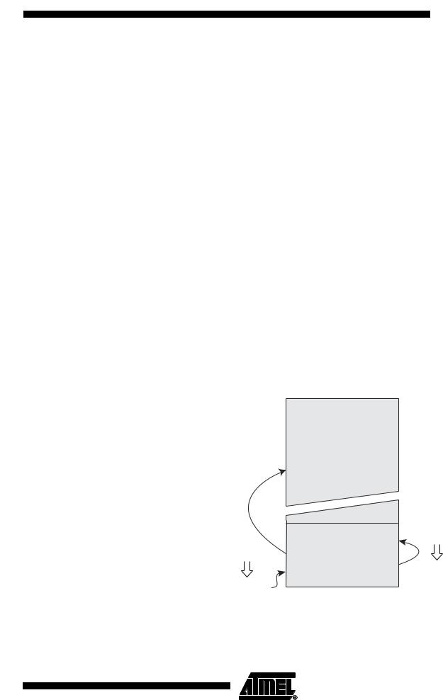
Figure 101. Read-While-Write vs. No Read-While-Write
Read-While-Write
(RWW) Section
|
Z-pointer |
|
Addresses NRWW |
Z-pointer |
section |
|
|
Addresses RWW |
No Read-While-Write |
section |
(NRWW) Section |
|
CPU is Halted |
Code Located in |
during the Operation |
|
|
NRWW Section |
|
Can be Read during |
|
the Operation |
|
207
2486M–AVR–12/03