

ATtiny25/45/85
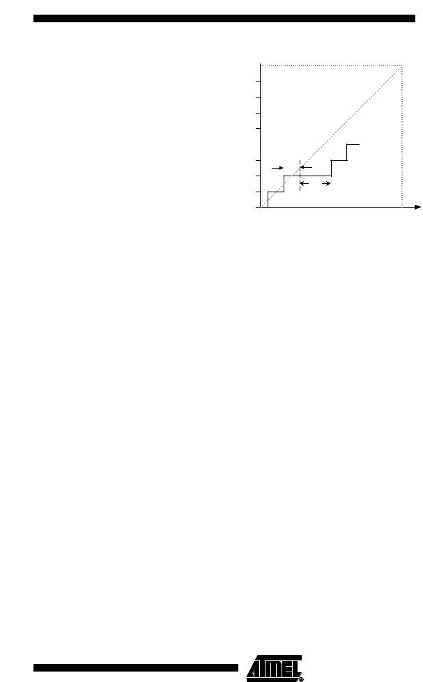
Figure 19-12. Differential Non-linearity (DNL)
Output Code
0x3FF
|
1 LSB |
|
DNL |
0x000 |
|
0 |
VREF Input Voltage |
•Quantization Error: Due to the quantization of the input voltage into a finite number of codes, a range of input voltages (1 LSB wide) will code to the same value. Always ± 0.5 LSB.
•Absolute Accuracy: The maximum deviation of an actual (unadjusted) transition compared to an ideal transition for any code. This is the compound effect of offset, gain error, differential error, non-linearity, and quantization error. Ideal value: ± 0.5 LSB.
19.7ADC Conversion Result
After the conversion is complete (ADIF is high), the conversion result can be found in the ADC Result Registers (ADCL, ADCH). The form of the conversion result depends on the type of the conversio as there are three types of conversions: single ended conversion, unipolar differential conversion and bipolar differential conversion.
19.7.1Single Ended Conversion
For single ended conversion, the result is
ADC VIN 1024
= --------------------------
VREF
where VIN is the voltage on the selected input pin and VREF the selected voltage reference (see Table 19-3 on page 137 and Table 19-4 on page 138). 0x000 represents analog ground, and 0x3FF represents the selected voltage reference minus one LSB. The result is presented in onesided form, from 0x3FF to 0x000.
19.7.2Unipolar Differential Conversion
If differential channels and an unipolar input mode are used, the result is
ADC (VPOS – VNEG) 1024 GAIN
= -------------------------------------------------------
VREF
where VPOS is the voltage on the positive input pin, VNEG the voltage on the negative input pin, and VREF the selected voltage reference (see Table 19-3 on page 137 and Table 19-4 on page
135
2586A–AVR–02/05

138). The voltage on the positive pin must always be larger than the voltage on the negative pin or otherwise the voltage difference is saturated to zero. The result is presented in one-sided form, from 0x000 (0d) to 0x3FF (+1023d). The GAIN is either 1x or 20x.
19.7.3Bipolar Differential Conversion
As default the ADC converter operates in the unipolar input mode, but the bipolar input mode can be selected by writting the BIN bit in the ADCSRB to one. In the bipolar input mode twosided voltage differences are allowed and thus the voltage on the negative input pin can also be larger than the voltage on the positive input pin. If differential channels and a bipolar input mode are used, the result is
ADC (VPOS – VNEG) 512 GAIN
= ----------------------------------------------------
VREF
where VPOS is the voltage on the positive input pin, VNEG the voltage on the negative input pin, and VREF the selected voltage reference. The result is presented in two’s complement form, from 0x200 (-512d) through 0x000 (+0d) to 0x1FF (+511d). The GAIN is either 1x or 20x.
However, if the signal is not bipolar by nature (9 bits + sign as the 10th bit), this scheme loses one bit of the converter dynamic range. Then, if the user wants to perform the conversion with the maximum dynamic range, the user can perform a quick polarity check of the result and use the unipolar differential conversion with selectable differential input pairs (see the Input Polarity Reversal mode ie. the IPR bit in the ADCSRB register on page 135). When the polarity check is performed, it is sufficient to read the MSB of the result (ADC9 in ADCH). If the bit is one, the result is negative, and if this bit is zero, the result is positive.
19.7.4Temperature Measurement (Preliminary description)
The temperature measurement is based on an on-chip temperature sensor that is coupled to a single ended ADC4 channel. Selecting the ADC4 channel by writing the MUX3..0 bits in ADMUX register to “1111” enables the temperature sensor. The internal 1.1V voltage reference must also be selected for the ADC voltage reference source in the temperature sensor measurement. When the temperature sensor is enabled, the ADC converter can be used in single conversion mode to measure the voltage over the temperature sensor.
The measured voltage has a linear relationship to the temperature as described in Table 51. The voltage sensitivity is approximately 1 mV / °C and the accuracy of the temperature measurement is +/- 10°C after bandgap calibration.
Table 19-2. Temperature vs. Sensor Output Voltage (Typical Case)
Temperature / °C |
-45 °C |
|
+25 °C |
|
+105 °C |
|
|
|
|
|
|
Voltage / mV |
|
242 mV |
|
314 mv |
403 mV |
|
|
|
|
|
|
The values described in Table 51 are typical values. However, due to the process variation the temperature sensor output voltage varies from one chip to another. To be capable of achieving more accurate results the temperature measurement can be calibrated in the application software. The software calibration requires that a calibration value is measured and stored in a register or EEPROM for each chip, as a part of the production test. The sofware calibration can be done utilizing the formula:
136 ATtiny25/45/85 
2586A–AVR–02/05

 ATtiny25/45/85
Temperature = k VTEMP + TOS
where VTEMP is the ADC reading of the temperature sensor signal, k is a fixed coefficient (TBD) and TOS is the temperature sensor offset value determined and stored into EEPROM as a part of production test.
19.7.5ADC Multiplexer Selection Register – ADMUX
Bit |
7 |
6 |
5 |
4 |
3 |
2 |
1 |
0 |
|
|
REFS1 |
REFS0 |
ADLAR |
REFS2 |
MUX3 |
MUX2 |
MUX1 |
MUX0 |
ADMUX |
|
|
|
|
|
|
|
|
|
|
Read/Write |
R |
R/W |
R/W |
R |
R |
R |
R/W |
R/W |
|
Initial Value |
0 |
0 |
0 |
0 |
0 |
0 |
0 |
0 |
|
• Bit 7..6,4 – REFS2..REFS0: Voltage Reference Selection Bits
These bits select the voltage reference (VREF) for the ADC, as shown in Table 19-3. If these bits are changed during a conversion, the change will not go in effect until this conversion is complete (ADIF in ADCSR is set). Whenever these bits are changed, the next conversion will take 25 ADC clock cycles. If active channels are used, using VCC or an external AREF higher than (VCC - 1V) as a voltage reference is not recommended, as this will affect the ADC accuracy.
Table 19-3. |
Voltage Reference Selections for ADC |
|||
REFS2 |
REFS1 |
REFS0 |
Voltage Reference (VREF) Selection |
|
0 |
0 |
0 |
VCC used as Voltage Reference, disconnected from PB0 (AREF). |
|
|
|
|
|
|
0 |
0 |
1 |
External Voltage Reference at PB0 (AREF) pin, Internal Voltage |
|
Reference turned off. |
||||
|
|
|
||
|
|
|
|
|
0 |
1 |
0 |
Internal 1.1V Voltage Reference without external bypass capacitor, |
|
disconnected from PB0 (AREF). |
||||
|
|
|
||
|
|
|
|
|
0 |
1 |
1 |
Internal 1.1V Voltage Reference with external bypass capacitor at |
|
PB0 (AREF) pin. |
||||
|
|
|
||
|
|
|
|
|
1 |
1 |
0 |
Internal 2.56V Voltage Reference without external bypass |
|
capacitor, disconnected from PB0 (AREF). |
||||
|
|
|
||
|
|
|
|
|
1 |
1 |
1 |
Internal 2.56V Voltage Reference with external bypass capacitor at |
|
PB0 (AREF) pin. |
||||
|
|
|
||
|
|
|
|
|
•Bit 5 – ADLAR: ADC Left Adjust Result
The ADLAR bit affects the presentation of the ADC conversion result in the ADC Data Register. Write one to ADLAR to left adjust the result. Otherwise, the result is right adjusted. Changing the ADLAR bit will affect the ADC Data Register immediately, regardless of any ongoing conversions. For a comple te description of this bit, see ”The ADC Data Register – ADCL and ADCH” on page 140.
• Bits 3:0 – MUX3:0: Analog Channel and Gain Selection Bits
The value of these bits selects which combination of analog inputs are connected to the ADC. In case of differential input (ADC0 - ADC1 or ADC2 - ADC3), gain selection is also made with these bits. Selecting ADC2 or ADC0 as both inputs to the differential gain stage enables offset measurements. Selecting the single-ended channel ADC4 enables the temperature sensor. Refer to
137
2586A–AVR–02/05

Table 19-4 for details. If these bits are changed during a conversion, the change will not go into effect until this conversion is complete (ADIF in ADCSRA is set).
Table 19-4. |
Input Channel Selections |
|
|
|
||
|
|
Single Ended |
|
Positive |
Negative |
|
MUX3..0 |
|
Input |
|
Differential Input |
Differential Input |
Gain |
|
|
|
|
|
|
|
0000 |
|
ADC0 (PB5) |
|
|
|
|
|
|
|
|
|
|
|
0001 |
|
ADC1 (PB2) |
|
|
N/A |
|
|
|
|
|
|
|
|
0010 |
|
ADC2 (PB3) |
|
|
|
|
|
|
|
|
|
||
|
|
|
|
|
|
|
0011 |
|
ADC3 (PB4) |
|
|
|
|
|
|
|
|
|
|
|
0100 |
|
|
|
ADC2 (PB3) |
ADC2 (PB3) |
1x |
|
|
|
|
|
|
|
0101 (1) |
|
|
|
ADC2 (PB3) |
ADC2 (PB3) |
20x |
0110 |
|
|
|
ADC2 (PB3) |
ADC3 (PB4) |
1x |
|
|
|
|
|
|
|
0111 |
|
N/A |
|
ADC2 (PB3) |
ADC3 (PB4) |
20x |
|
|
|
|
|
|
|
1000 |
|
|
ADC0 (PB5) |
ADC0 (PB5) |
1x |
|
|
|
|
||||
|
|
|
|
|
|
|
1001 |
|
|
|
ADC0 (PB5) |
ADC0 (PB5) |
20x |
|
|
|
|
|
|
|
1010 |
|
|
|
ADC0 (PB5) |
ADC1 (PB2) |
1x |
|
|
|
|
|
|
|
1011 |
|
|
|
ADC0 (PB5) |
ADC1 (PB2) |
20x |
|
|
|
|
|
|
|
1100 |
|
1.1V/2.56V |
|
|
|
|
|
|
|
|
|
|
|
1101 |
|
0V |
|
|
N/A |
|
|
|
|
|
|
|
|
1110 |
|
N/A |
|
|
|
|
|
|
|
|
|
||
|
|
|
|
|
|
|
1111 |
|
ADC4 (2) |
|
|
|
|
1.For offset calibration only . See Section “19.2” on page 126.
2.For Temperature Sensor
19.7.6ADC Control and Status Register A – ADCSRA
Bit |
7 |
6 |
5 |
4 |
3 |
2 |
1 |
0 |
|
|
ADEN |
ADSC |
ADATE |
ADIF |
ADIE |
ADPS2 |
ADPS1 |
ADPS0 |
ADCSRA |
|
|
|
|
|
|
|
|
|
|
Read/Write |
R/W |
R/W |
R/W |
R/W |
R/W |
R/W |
R/W |
R/W |
|
Initial Value |
0 |
0 |
0 |
0 |
0 |
0 |
0 |
0 |
|
• Bit 7 – ADEN: ADC Enable
Writing this bit to one enables the ADC. By writing it to zero, the ADC is turned off. Turning the ADC off while a conversion is in progress, will terminate this conversion.
• Bit 6 – ADSC: ADC Start Conversion
In Single Conversion mode, write this bit to one to start each conversion. In Free Running mode, write this bit to one to start the first conversion. The first conversion after ADSC has been written after the ADC has been enabled, or if ADSC is written at the same time as the ADC is enabled, will take 25 ADC clock cycles instead of the normal 13. This first conversion performs initialization of the ADC.
ADSC will read as one as long as a conversion is in progress. When the conversion is complete, it returns to zero. Writing zero to this bit has no effect.
138 ATtiny25/45/85 
2586A–AVR–02/05

ATtiny25/45/85
• Bit 5 – ADATE: ADC Auto Trigger Enable
When this bit is written to one, Auto Triggering of the ADC is enabled. The ADC will start a conversion on a positive edge of the selected trigger signal. The trigger source is selected by setting the ADC Trigger Select bits, ADTS in ADCSRB.
• Bit 4 – ADIF: ADC Interrupt Flag
This bit is set when an ADC conversion completes and the data registers are updated. The ADC Conversion Complete Interrupt is executed if the ADIE bit and the I-bit in SREG are set. ADIF is cleared by hardware when executing the corresponding interrupt handling vector. Alternatively, ADIF is cleared by writing a logical one to the flag. Beware that if doing a Read-Modify-Write on ADCSRA, a pending interrupt can be disabled. This also applies if the SBI and CBI instructions are used.
• Bit 3 – ADIE: ADC Interrupt Enable
When this bit is written to one and the I-bit in SREG is set, the ADC Conversion Complete Interrupt is activated.
• Bits 2:0 – ADPS2:0: ADC Prescaler Select Bits
These bits determine the division factor between the system clock frequency and the input clock to the ADC.
Table 19-5. |
ADC Prescaler Selections |
|
|
||
ADPS2 |
|
ADPS1 |
|
ADPS0 |
Division Factor |
|
|
|
|
|
|
0 |
|
0 |
|
0 |
2 |
|
|
|
|
|
|
0 |
|
0 |
|
1 |
2 |
|
|
|
|
|
|
0 |
|
1 |
|
0 |
4 |
|
|
|
|
|
|
0 |
|
1 |
|
1 |
8 |
|
|
|
|
|
|
1 |
|
0 |
|
0 |
16 |
|
|
|
|
|
|
1 |
|
0 |
|
1 |
32 |
|
|
|
|
|
|
1 |
|
1 |
|
0 |
64 |
|
|
|
|
|
|
1 |
|
1 |
|
1 |
128 |
|
|
|
|
|
|
139
2586A–AVR–02/05