
- •1 STM32Cube overview
- •2 Getting started with STM32CubeMX
- •2.1 Principles
- •2.2 Key features
- •2.3 Rules and limitations
- •3 Installing and running STM32CubeMX
- •3.1 System requirements
- •3.1.1 Supported operating systems and architectures
- •3.1.2 Memory prerequisites
- •3.1.3 Software requirements
- •Java™ Runtime Environment
- •macOS software requirements
- •3.2 Installing/uninstalling STM32CubeMX standalone version
- •3.2.1 Installing STM32CubeMX standalone version
- •3.2.2 Installing STM32CubeMX from command line
- •Interactive mode
- •Auto-install mode
- •3.2.3 Uninstalling STM32CubeMX standalone version
- •Uninstalling STM32CubeMX on macOS®
- •Uninstalling STM32CubeMX on Linux®
- •Uninstalling STM32CubeMX on Windows®
- •3.3 Launching STM32CubeMX
- •3.3.1 Running STM32CubeMX as a standalone application
- •3.4 Getting updates using STM32CubeMX
- •3.4.1 Running STM32CubeMX behind a proxy server
- •3.4.2 Updater configuration
- •3.4.3 Installing STM32 MCU packages
- •3.4.4 Installing STM32 MCU package patches
- •3.4.5 Installing embedded software packs
- •3.4.6 Removing already installed embedded software packages
- •3.4.7 Checking for updates
- •4 STM32CubeMX user interface
- •4.1 Home page
- •4.1.1 File menu
- •Table 2. Home page shortcuts
- •4.1.2 Window menu and Outputs tabs
- •Table 3. Window menu
- •4.1.3 Help menu
- •Table 4. Help menu shortcuts
- •4.1.4 Social links
- •4.2 New Project window
- •4.2.1 MCU selector
- •MCU selection
- •Export to Excel feature
- •Show favorite MCUs feature
- •MCU close selector feature
- •4.2.2 Board selector
- •4.2.3 Example selector
- •4.2.4 Cross selector
- •Part number selection
- •Compare cart
- •MCU/MPU selection for a new project
- •4.3 Project page
- •4.4 Pinout & Configuration view
- •Tips
- •4.4.1 Component list
- •Contextual help
- •Icons and color schemes
- •4.4.2 Component Mode panel
- •4.4.3 Pinout view
- •Tips and tricks
- •4.4.4 Pinout menu and shortcuts
- •4.4.5 Pinout view advanced actions
- •Manually modifying pin assignments
- •Manually remapping a function to another pin
- •Manual remapping with destination pin ambiguity
- •Resolving pin conflicts
- •4.4.6 Keep Current Signals Placement
- •Keep Current Signals Placement is unchecked
- •Keep Current Signals Placement is checked
- •4.4.7 Pinning and labeling signals on pins
- •4.4.8 Pinout for multi-bonding packages
- •4.4.9 System view
- •Table 7. Configuration states
- •4.4.10 Component configuration panel
- •Table 8. Peripheral and Middleware configuration window buttons and tooltips
- •No check option
- •4.4.11 User Constants configuration window
- •Creating/editing user constants
- •Deleting user constants
- •Searching for user constants
- •4.4.12 GPIO configuration window
- •4.4.13 DMA configuration window
- •4.4.14 NVIC configuration window
- •Enabling interruptions using the NVIC tab view
- •Code generation options for interrupt handling
- •4.4.15 FreeRTOS configuration panel
- •Tasks and Queues Tab
- •Timers, Mutexes and Semaphores
- •FreeRTOS heap usage
- •4.4.16 Setting HAL timebase source
- •Example of configuration using SysTick without FreeRTOS
- •Example of configuration using SysTick and FreeRTOS
- •Example of configuration using TIM2 as HAL timebase source
- •4.5 Pinout & Configuration view for STM32MP1 series
- •4.5.1 Run time configuration
- •4.5.2 Boot stages configuration
- •Boot ROM peripherals selection
- •Boot loader (A7 FSBL) peripherals selection
- •4.7 Enabling security in Pinout & Configuration view (STM32L5 and STM32U5 series only)
- •4.7.1 Privilege access for peripherals, GPIO EXTIs and DMA requests
- •4.7.3 NVIC and context assignment for peripherals interrupts
- •4.7.4 DMA (context assignment and privilege access settings)
- •4.7.5 GTZC
- •4.7.6 OTFDEC
- •4.8 Clock Configuration view
- •4.8.1 Clock tree configuration functions
- •External clock sources
- •Peripheral clock configuration options
- •Table 9. Clock configuration view widgets
- •4.8.2 Securing clock resources (STM32L5 series only)
- •4.8.3 Recommendations
- •Table 11. Voltage scaling versus power over-drive and HCLK frequency
- •Table 12. Relations between power over-drive and HCLK frequency
- •4.8.5 Clock tree glossary
- •4.9 Project Manager view
- •4.9.1 Project tab
- •4.9.2 Code Generator tab
- •STM32Cube Firmware Library Package option
- •Generated files options
- •HAL settings options
- •Custom code template options
- •4.9.3 Advanced Settings tab
- •Choosing not to generate code for some peripherals or middlewares
- •Ordering initialization function calls
- •Disabling calls to initialization functions
- •Choosing between HAL and LL based code generation for a given peripheral instance
- •4.10 Import Project window
- •4.11 Set unused / Reset used GPIOs windows
- •4.12 Update Manager windows
- •4.13 Software Packs component selection window
- •4.13.1 Introduction on software components
- •4.13.2 Filter panel
- •Table 14. Additional software window - Filter icons
- •4.13.3 Packs panel
- •Table 15. Additional Software window – Packs panel columns
- •4.13.4 Component dependencies panel
- •Table 17. Component dependencies panel contextual help
- •4.13.5 Details and Warnings panel
- •4.13.6 Updating the tree view for additional software components
- •4.14 LPBAM Scenario & Configuration view
- •4.15 CAD Resources view section
- •Access from MCU selector
- •Access from STM32CubeMX project view
- •4.16 Boot path
- •4.16.1 Available boot paths
- •Table 18. Boot paths without TrustZone (TZEN = 0)
- •Table 19. Boot paths with TrustZone (TZEN = 1)
- •4.16.2 Creating a boot path project: an example
- •Step 1: Selecting the MCU
- •Step 2: Project creation with OEM-iRoT boot path
- •Step 3: Device and peripherals configuration
- •Step 4: Overall configuration
- •Step 5: Boot path selection
- •Step 6: Authentication and encryption keys regeneration, option byte file generation
- •Step 7: Code generation
- •Step 8: Code compilation and encrypted binaries generation
- •Step 9: Provisioning of the board
- •Step 1: Generating the code
- •Step 2: Code compilation and encrypted binaries generation
- •ST-iRoT board provisioning
- •Step 1: SMAK code generation
- •SMAK code compilation and encrypted binaries generation
- •Secure manager API
- •4.16.6 How to configure an assembled boot path
- •Step 1: Configure flash_layout.h file
- •Step 2: Compile OEMiROT_Boot project
- •Step 3: Compile OEMiROT_Boot project
- •4.17 User authentication
- •4.17.1 Login with an existing my.st.com account
- •4.17.2 Create a my.st.com account
- •4.17.3 Authentication through command line interface
- •4.18 STM32CubeMX Memory Management Tool
- •Feature: MMT usage, Pinout, and Configuration UI
- •Feature: MMT usage and linker script
- •User interface
- •Region information
- •Code generation configuration
- •Apply Application Regions settings to linker files
- •Configuring an external memory
- •Configuring a memory region using the left panel
- •Setting up a middleware memory location
- •Remap
- •Code generation
- •4.19 About window
- •5 STM32CubeMX tools
- •5.1 External Tools
- •5.2 Power Consumption Calculator view
- •5.2.1 Building a power consumption sequence
- •Selecting a VDD value
- •Selecting a battery model (optional)
- •Power sequence default view
- •Managing sequence steps
- •Adding a step
- •Editing a step
- •Moving a step
- •Deleting a step
- •Using the transition checker
- •5.2.2 Configuring a step in the power sequence
- •Using interpolation
- •Importing pinout
- •Selecting/deselecting all peripherals
- •Managing the whole sequence (load, save and compare)
- •Managing the results charts and display options
- •Overview of the Results summary area
- •5.2.4 Power sequence step parameters glossary
- •5.2.5 Battery glossary
- •5.2.6 SMPS feature
- •5.2.7 BLE and ZigBee support (STM32WB series only)
- •5.3 DDR Suite (for STM32MP1 series only)
- •5.3.1 DDR configuration
- •DDR type, width and density
- •DDR configuration
- •DDR3 configuration
- •5.3.2 Connection to the target and DDR register loading
- •Prerequisites
- •Connection to the target
- •Output/Log messages
- •DDR register loading (optional)
- •5.3.3 DDR testing
- •Prerequisites
- •DDR test list
- •DDR test results
- •6 STM32CubeMX C Code generation overview
- •6.1 STM32Cube code generation using only HAL drivers (default mode)
- •6.2 STM32Cube code generation using Low Layer drivers
- •Table 20. LL versus HAL code generation: drivers included in STM32CubeMX projects
- •Table 21. LL versus HAL code generation: STM32CubeMX generated header files
- •Table 22. LL versus HAL: STM32CubeMX generated source files
- •6.3 Custom code generation
- •6.3.1 STM32CubeMX data model for FreeMarker user templates
- •6.3.2 Saving and selecting user templates
- •6.3.3 Custom code generation
- •6.4 Additional settings for C project generation
- •Possible entries and syntax
- •.extSettings file example and generated outcomes
- •[Groups]
- •[Others]
- •7 Code generation for dual-core MCUs (STM32H7 dual-core product lines only)
- •Generated initialization code
- •Generated startup and linker files
- •Generated boot mode code
- •8 Code generation with TrustZone® enabled (STM32L5 series only)
- •Specificities
- •9 Device tree generation (STM32MP1 series only)
- •9.1 Device tree overview
- •9.2 STM32CubeMX Device tree generation
- •10 Support of additional software components using CMSIS-Pack standard
- •11 Tutorial 1: From pinout to project C code generation using an MCU of the STM32F4 series
- •11.1 Creating a new STM32CubeMX Project
- •11.2 Configuring the MCU pinout
- •11.3 Saving the project
- •11.4 Generating the report
- •11.5 Configuring the MCU clock tree
- •11.6 Configuring the MCU initialization parameters
- •11.6.1 Initial conditions
- •11.6.2 Configuring the peripherals
- •11.6.3 Configuring the GPIOs
- •11.6.4 Configuring the DMAs
- •11.6.5 Configuring the middleware
- •11.7 Generating a complete C project
- •11.7.1 Setting project options
- •11.7.2 Downloading firmware package and generating the C code
- •11.8 Building and updating the C code project
- •11.9 Switching to another MCU
- •12 Tutorial 2 - Example of FatFs on an SD card using STM32429I-EVAL evaluation board
- •13 Tutorial 3 - Using the Power Consumption Calculator to optimize the embedded application consumption and more
- •13.1 Tutorial overview
- •13.2 Application example description
- •13.3 Using the Power Consumption Calculator
- •13.3.1 Creating a power sequence
- •13.3.2 Optimizing application power consumption
- •Step 1 (Run)
- •Step 4 (Run, RTC)
- •Step 5 (Run, ADC, DMA, RTC)
- •Step 6 (Sleep, DMA, ADC, RTC)
- •Step 7 (Run, DMA, RTC, USART)
- •Step 8 (Stop 0, USART)
- •Step 10 (RTC, USART)
- •14 Tutorial 4 - Example of UART communications with an STM32L053xx Nucleo board
- •14.1 Tutorial overview
- •14.2 Creating a new STM32CubeMX project and selecting the Nucleo board
- •14.3 Selecting the features from the Pinout view
- •14.4 Configuring the MCU clock tree from the Clock Configuration view
- •14.5 Configuring the peripheral parameters from the Configuration view
- •14.6 Configuring the project settings and generating the project
- •14.7 Updating the project with the user application code
- •14.8 Compiling and running the project
- •14.9 Configuring Tera Term software as serial communication client on the PC
- •15 Tutorial 5: Exporting current project configuration to a compatible MCU
- •16 Tutorial 6 – Adding embedded software packs to user projects
- •17 Tutorial 7 – Using the X-Cube-BLE1 software pack
- •Table 25. Connection with hardware resources
- •18 Creating LPBAM projects
- •18.1 LPBAM overview
- •18.1.1 LPBAM operating mode
- •18.1.2 LPBAM firmware
- •18.1.3 Supported series
- •18.1.4 LPBAM design
- •18.1.5 LPBAM project support in STM32CubeMX
- •18.2 Creating an LPBAM project
- •18.2.1 LPBAM feature availability
- •18.2.2 Describing an LPBAM project
- •18.2.3 Managing LPBAM applications in a project
- •18.3 Describing an LPBAM application
- •18.3.1 Overview (SoC & IPs configuration, runtime scenario)
- •SoC and IPs configuration
- •Runtime description (scenario)
- •18.3.2 SoC& IPs: configuring the clock
- •18.3.3 SoC & IPs: configuring the IPs
- •18.3.4 SoC & IPs: configuring Low Power settings
- •18.3.5 LPBAM scenario: managing queues
- •18.3.6 Queue description: managing nodes
- •18.3.7 Queue description: configuring the queue in circular mode
- •18.3.8 Queue description: configuring the DMA channel hosting the queue
- •Basic configuration
- •DMA channel NVIC configuration
- •18.3.9 Node description: accessing contextual help and documentation
- •18.3.10 Node description: configuring node parameters
- •18.3.11 Node description: configuring a trigger
- •18.3.12 Node description: reconfiguring a DMA for Data transfer
- •18.4 Checking the LPBAM design
- •18.5 Generating a project with LPBAM applications
- •18.6 LPBAM application for TrustZone activated projects
- •STM32CubeMX standard project view
- •STM32CubeMX LPBAM view
- •Security settings coherency check
- •19.1 I encountered a network connection error during a download from STM32CubeMX.
- •19.2 Since I changed my login to access the Internet, some software packs appear not available.
- •19.4 On the Pinout configuration panel, why does STM32CubeMX move some functions when I add a new peripheral mode?
- •19.5 How can I manually force a function remapping?
- •19.6 Why some pins are highlighted in yellow or in light green in the Pinout view? Why I cannot change the function of some pins (when I click some pins, nothing happens)?
- •19.7 Why does the RTC multiplexer remain inactive on the Clock tree view?
- •19.8 How can I select LSE and HSE as clock source and change the frequency?
- •19.9 Why STM32CubeMX does not allow me to configure PC13, PC14, PC15, and PI8 as outputs when one of them is already configured as an output?
- •19.10 Ethernet configuration: why cannot I specify DP83848 or LAN8742A in some cases?
- •19.11 How to fix MX_DMA_Init call rank in STM32CubeMX generated projects?
- •19.12 When is the PeriphCommonClock_Config() function generated?
- •Appendix A STM32CubeMX pin assignment rules
- •A.1 Block consistency
- •Example of block mapping with an STM32F107x MCU
- •Example of block remapping with an STM32F107x MCU
- •A.2 Block inter-dependency
- •Example of block remapping of SPI in full-duplex master mode with an STM32F107x MCU
- •A.3 One block = one peripheral mode
- •Example of STM32F107x MCU
- •A.4 Block remapping (STM32F10x only)
- •Example
- •A.5 Function remapping
- •Example using STM32F415x
- •A.6 Block shifting (only for STM32F10x and when “Keep Current Signals placement” is unchecked)
- •Example
- •A.7 Setting and clearing a peripheral mode
- •A.8 Mapping a function individually
- •A.9 GPIO signals mapping
- •Appendix B STM32CubeMX C code generation design choices and limitations
- •B.2 STM32CubeMX design choices for peripheral initialization
- •B.3 STM32CubeMX design choices and limitations for middleware initialization
- •B.3.1 Overview
- •B.3.5 FreeRTOS
- •B.3.6 LwIP
- •B.3.7 Libjpeg
- •B.3.8 Mbed TLS
- •B.3.9 TouchSensing
- •B.3.11 STM32WPAN BLE/Thread (STM32WB series only)
- •BLE configuration
- •Thread configuration
- •B.3.12 CMSIS packs selection limitation
- •Appendix C STM32 microcontrollers naming conventions
- •Appendix D STM32 microcontrollers power consumption parameters
- •D.1 Power modes
- •D.1.1 STM32L1 series
- •D.1.3 STM32L0 series
- •D.2 Power consumption ranges
- •D.2.1 STM32L1 series features three VCORE ranges
- •D.2.2 STM32F4 series features several VCORE scales
- •D.2.3 STM32L0 series features three VCORE ranges
- •Appendix E STM32Cube embedded software packages
- •Revision history

Tutorial 1: From pinout to project C code generation using an MCU of the STM32F4 series
|
3. Keep the core and peripheral clocks to 16 MHz using HSI, no PLL and no prescaling. |
Note: |
Optionally, further adjust the system and peripheral clocks using PLL, prescalers and |
|
multipliers: |
|
Other clock sources independent from the system clock can be configured as follows: |
–USB OTG FS, Random Number Generator and SDIO clocks are driven by an independent output of the PLL.
–I2S peripherals come with their own internal clock (PLLI2S), alternatively derived by an independent external clock source.
–USB OTG HS and Ethernet Clocks are derived from an external source.
4.Optionally, configure the prescaler for the Microcontroller Clock Output (MCO) pins that allow to output two clocks to the external circuit.
5.Click to save the project.
6.Go to the Configuration tab to proceed with the project configuration.
11.6Configuring the MCU initialization parameters
Caution: The C code generated by STM32CubeMX covers the initialization of the MCU peripherals and middlewares using the STM32Cube firmware libraries.
11.6.1Initial conditions
|
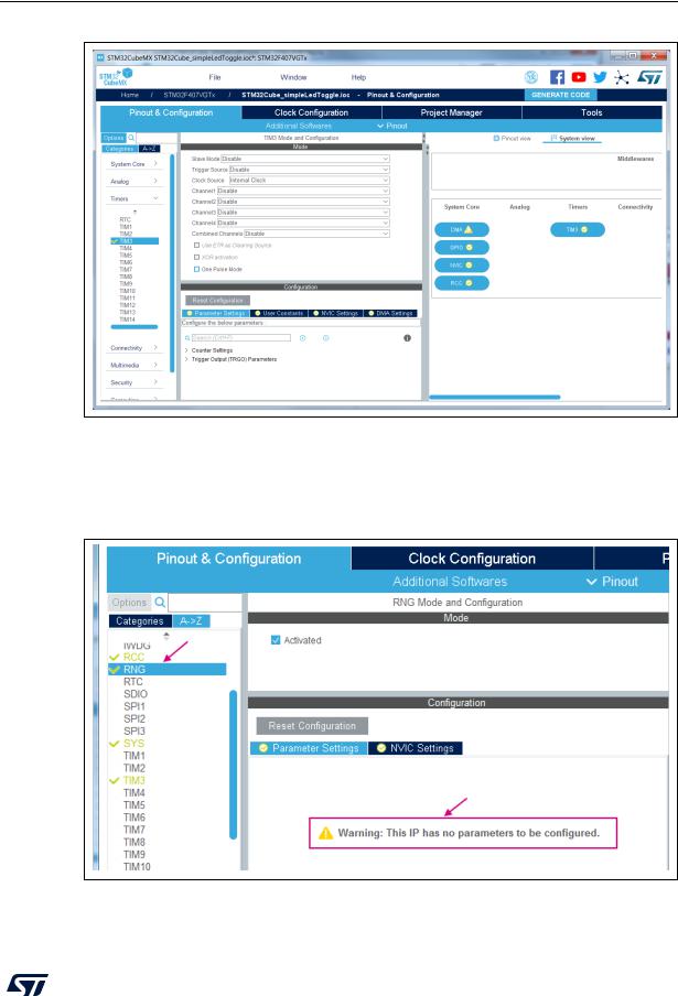
From the Pinout & Configuration tab, select and configure (one by one) every component |
|
(peripheral, middleware, additional software) required by the application using the Mode |
|
and Configuration panels (see Figure 319). |
|
Tooltips and warning messages are displayed when peripherals are not properly configured |
|
(see Section 4: STM32CubeMX user interface for details). |
Note: |
The RCC peripheral initialization will use the parameter configuration done in this view as |
|
well as the configuration done in the Clock tree view (clock source, frequencies, prescaler |
|
values, etc…). |
296/453 |
UM1718 Rev 41 |

UM1718Tutorial 1: From pinout to project C code generation using an MCU of the STM32F4 series
Figure 319. Pinout & Configuration view
11.6.2Configuring the peripherals
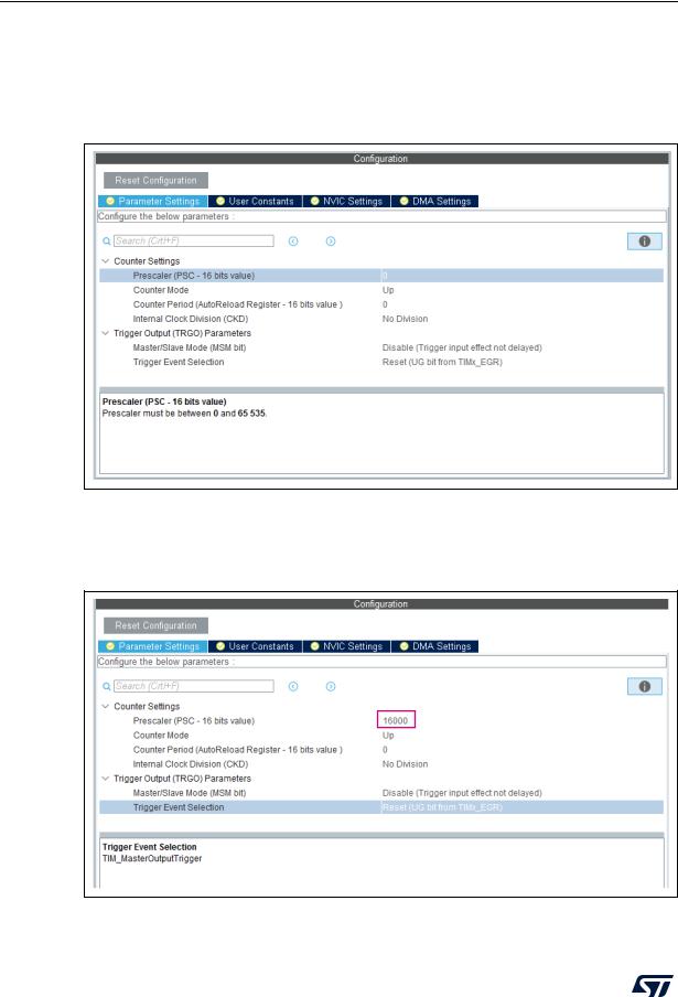
Each peripheral instance corresponds to a dedicated button in the main panel. Some peripheral modes have no configurable parameters, as illustrated below.
Figure 320. Case of Peripheral and Middleware without configuration parameters
UM1718 Rev 41 |
297/453 |

Tutorial 1: From pinout to project C code generation using an MCU of the STM32F4 series
Follow the steps below to proceed with peripheral configuration:
1.Click the peripheral button to open the corresponding configuration window. In our example
a)click TIM3 to open the timer configuration window.
Figure 321. Timer 3 configuration window
b)with a 16 MHz APB clock (Clock tree view), set the prescaler to 16000 and the counter period to 1000 to make the LED blink every millisecond.
Figure 322. Timer 3 configuration
298/453 |
UM1718 Rev 41 |

UM1718Tutorial 1: From pinout to project C code generation using an MCU of the STM32F4 series
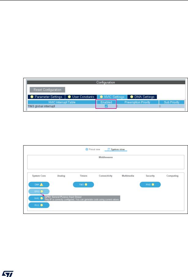
2.Optionally, and when available, select:
–The NVIC Settings tab to display the NVIC configuration and enable interruptions for this peripheral.
–The DMA Settings tab to display the DMA configuration and to configure DMA transfers for this peripheral.
In the tutorial example, the DMA is not used and the GPIO settings remain unchanged. The interrupt is enabled, as shown in Figure 323.
–The GPIO Settings tab to display the GPIO configuration and to configure the GPIOs for this peripheral.
–Insert an item:
–The User Constants tab to specify constants to be used in the project.
Figure 323. Enabling Timer 3 interrupt
11.6.3Configuring the GPIOs
The user can adjust all pin configurations from this window. A small icon along with a tooltip indicates the configuration status.
Figure 324. GPIO configuration color scheme and tooltip
UM1718 Rev 41 |
299/453 |

Tutorial 1: From pinout to project C code generation using an MCU of the STM32F4 series
Follow the sequence below to configure the GPIOs:
1.Click the GPIO button in the Configuration view to open the Pin Configuration window below.
2.The first tab shows the pins that have been assigned a GPIO mode but not for a dedicated peripheral and middleware. Select a Pin Name to open the configuration for that pin.
In the tutorial example, select PD12 and configure it in output push-pull mode to drive the STM32F4DISCOVERY LED (see Figure 325).
Figure 325. GPIO mode configuration
300/453 |
UM1718 Rev 41 |