


STM32CubeMX tools |
UM1718 |
|
|
5.2.2Configuring a step in the power sequence
The step configuration is performed from the Edit Step and New Step windows. The graphical interface guides the user by forcing a predefined order for setting parameters.
Their naming may differ according to the selected MCU series. For details on each parameter, refer to glossary in Section 5.2.4 and to Appendix D: STM32 microcontrollers power consumption parameters, or to the electrical characteristics section of the datasheet.
The parameters are set automatically by the tool when there is only one possible value (in this case, the parameter cannot be modified and is grayed out). The tool proposes only the configuration choices relevant to the selected MCU.
To configure a new step:
1.Click Add or Duplicate to open the New step window or double-click a step from the sequence table to open the Edit step window.
2.Within the open step window, select in the following order:
–The Power Mode
Changing the Power Mode resets the whole step configuration.
–The Peripherals
Peripherals can be selected/deselected at any time after the Power Mode is configured.
–The Power scale
The power scale corresponds to the power consumption range (STM32L1) or the power scale (STM32F4).
Changing the Power Mode or the Power Consumption Range discards all subsequent configurations.
–The Memory Fetch Type
–The VDD value if multiple choices available
–The voltage source (battery or VBUS)
–A Clock Configuration
Changing the Clock Configuration resets the frequency choices further down.
–When multiple choices are available, the CPU Frequency (STM32F4) and the AHB Bus Frequency/CPU Frequency(STM32L1) or, for active modes, a user specified frequency. In this case, the consumption value will be interpolated (see
Using interpolation).
3.Optionally set
–A step duration (1 ms is the default value)
–An additional consumption value (expressed in mA) to reflect, for example, external components used by the application (external regulator, external pull-up, LEDs or other displays). This value added to the microcontroller power consumption will impact the step overall power consumption.
4.Once the configuration is complete, the Add button becomes active. Click it to create the step and add it to the sequence table.
232/453 |
UM1718 Rev 41 |
UM1718 |
STM32CubeMX tools |
|
|
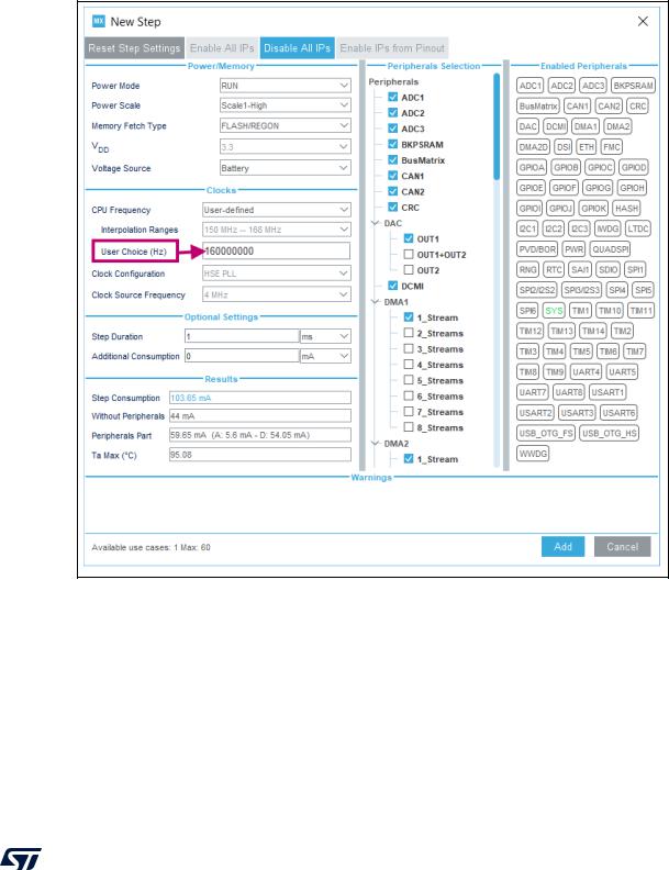
Using interpolation
For steps configured for active modes (Run, Sleep), frequency interpolation is supported by selecting CPU frequency as User Defined and entering a frequency in Hz (see Figure 246).
Figure 246. Interpolated power consumption
UM1718 Rev 41 |
233/453 |
STM32CubeMX tools |
UM1718 |
|
|
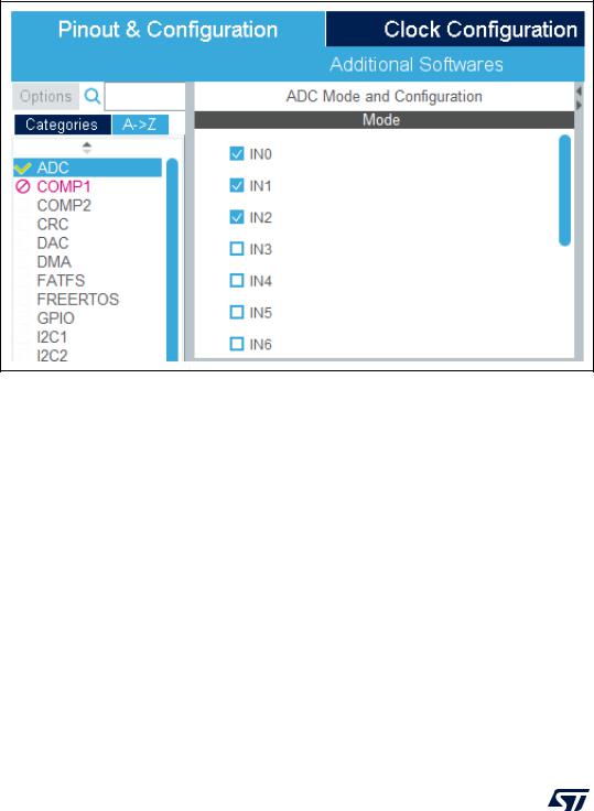
Importing pinout
Figure 247 illustrates the example of the ADC configuration in the Pinout view: clicking Enable IPs from Pinout in the Power Consumption Calculator view selects the ADC peripheral and GPIO A (Figure 248).
The Enable IPs from Pinout button allows the user to automatically select the peripherals that have been configured in the Pinout view.
Figure 247. ADC selected in Pinout view
234/453 |
UM1718 Rev 41 |

UM1718 |
STM32CubeMX tools |
|
|
Selecting/deselecting all peripherals
Clicking Enable All IPs allows the user to select all peripherals at once.
Clicking Disable All IPs removes them as contributors to the consumption.
Figure 248. Power Consumption Calculator Step configuration window:
ADC enabled using import pinout
5.2.3Managing user-defined power sequence and reviewing results
The configuration of a power sequence leads to an update of the Power Consumption Calculator view (see Figure 249):
•The sequence table shows all steps and step parameters values. A category column indicates whether the consumption values are taken from the datasheet or are interpolated.
•The sequence chart area shows different views of the power sequence according to a display type (e.g. plot all steps, plot low power versus run modes)
•The results summary provides the total sequence time, the maximum ambient
temperature (TAMAX), plus an estimate of the average power consumption, DMIPS, and battery lifetime provided a valid battery configuration has been selected.
UM1718 Rev 41 |
235/453 |