

- •1 STM32Cube overview
- •2 Getting started with STM32CubeMX
- •2.1 Principles
- •2.2 Key features
- •2.3 Rules and limitations
- •3 Installing and running STM32CubeMX
- •3.1 System requirements
- •3.1.1 Supported operating systems and architectures
- •3.1.2 Memory prerequisites
- •3.1.3 Software requirements
- •Java™ Runtime Environment
- •macOS software requirements
- •3.2 Installing/uninstalling STM32CubeMX standalone version
- •3.2.1 Installing STM32CubeMX standalone version
- •3.2.2 Installing STM32CubeMX from command line
- •Interactive mode
- •Auto-install mode
- •3.2.3 Uninstalling STM32CubeMX standalone version
- •Uninstalling STM32CubeMX on macOS®
- •Uninstalling STM32CubeMX on Linux®
- •Uninstalling STM32CubeMX on Windows®
- •3.3 Launching STM32CubeMX
- •3.3.1 Running STM32CubeMX as a standalone application
- •3.4 Getting updates using STM32CubeMX
- •3.4.1 Running STM32CubeMX behind a proxy server
- •3.4.2 Updater configuration
- •3.4.3 Installing STM32 MCU packages
- •3.4.4 Installing STM32 MCU package patches
- •3.4.5 Installing embedded software packs
- •3.4.6 Removing already installed embedded software packages
- •3.4.7 Checking for updates
- •4 STM32CubeMX user interface
- •4.1 Home page
- •4.1.1 File menu
- •Table 2. Home page shortcuts
- •4.1.2 Window menu and Outputs tabs
- •Table 3. Window menu
- •4.1.3 Help menu
- •Table 4. Help menu shortcuts
- •4.1.4 Social links
- •4.2 New Project window
- •4.2.1 MCU selector
- •MCU selection
- •Export to Excel feature
- •Show favorite MCUs feature
- •MCU close selector feature
- •4.2.2 Board selector
- •4.2.3 Example selector
- •4.2.4 Cross selector
- •Part number selection
- •Compare cart
- •MCU/MPU selection for a new project
- •4.3 Project page
- •4.4 Pinout & Configuration view
- •Tips
- •4.4.1 Component list
- •Contextual help
- •Icons and color schemes
- •4.4.2 Component Mode panel
- •4.4.3 Pinout view
- •Tips and tricks
- •4.4.4 Pinout menu and shortcuts
- •4.4.5 Pinout view advanced actions
- •Manually modifying pin assignments
- •Manually remapping a function to another pin
- •Manual remapping with destination pin ambiguity
- •Resolving pin conflicts
- •4.4.6 Keep Current Signals Placement
- •Keep Current Signals Placement is unchecked
- •Keep Current Signals Placement is checked
- •4.4.7 Pinning and labeling signals on pins
- •4.4.8 Pinout for multi-bonding packages
- •4.4.9 System view
- •Table 7. Configuration states
- •4.4.10 Component configuration panel
- •Table 8. Peripheral and Middleware configuration window buttons and tooltips
- •No check option
- •4.4.11 User Constants configuration window
- •Creating/editing user constants
- •Deleting user constants
- •Searching for user constants
- •4.4.12 GPIO configuration window
- •4.4.13 DMA configuration window
- •4.4.14 NVIC configuration window
- •Enabling interruptions using the NVIC tab view
- •Code generation options for interrupt handling
- •4.4.15 FreeRTOS configuration panel
- •Tasks and Queues Tab
- •Timers, Mutexes and Semaphores
- •FreeRTOS heap usage
- •4.4.16 Setting HAL timebase source
- •Example of configuration using SysTick without FreeRTOS
- •Example of configuration using SysTick and FreeRTOS
- •Example of configuration using TIM2 as HAL timebase source
- •4.5 Pinout & Configuration view for STM32MP1 series
- •4.5.1 Run time configuration
- •4.5.2 Boot stages configuration
- •Boot ROM peripherals selection
- •Boot loader (A7 FSBL) peripherals selection
- •4.7 Enabling security in Pinout & Configuration view (STM32L5 and STM32U5 series only)
- •4.7.1 Privilege access for peripherals, GPIO EXTIs and DMA requests
- •4.7.3 NVIC and context assignment for peripherals interrupts
- •4.7.4 DMA (context assignment and privilege access settings)
- •4.7.5 GTZC
- •4.7.6 OTFDEC
- •4.8 Clock Configuration view
- •4.8.1 Clock tree configuration functions
- •External clock sources
- •Peripheral clock configuration options
- •Table 9. Clock configuration view widgets
- •4.8.2 Securing clock resources (STM32L5 series only)
- •4.8.3 Recommendations
- •Table 11. Voltage scaling versus power over-drive and HCLK frequency
- •Table 12. Relations between power over-drive and HCLK frequency
- •4.8.5 Clock tree glossary
- •4.9 Project Manager view
- •4.9.1 Project tab
- •4.9.2 Code Generator tab
- •STM32Cube Firmware Library Package option
- •Generated files options
- •HAL settings options
- •Custom code template options
- •4.9.3 Advanced Settings tab
- •Choosing not to generate code for some peripherals or middlewares
- •Ordering initialization function calls
- •Disabling calls to initialization functions
- •Choosing between HAL and LL based code generation for a given peripheral instance
- •4.10 Import Project window
- •4.11 Set unused / Reset used GPIOs windows
- •4.12 Update Manager windows
- •4.13 Software Packs component selection window
- •4.13.1 Introduction on software components
- •4.13.2 Filter panel
- •Table 14. Additional software window - Filter icons
- •4.13.3 Packs panel
- •Table 15. Additional Software window – Packs panel columns
- •4.13.4 Component dependencies panel
- •Table 17. Component dependencies panel contextual help
- •4.13.5 Details and Warnings panel
- •4.13.6 Updating the tree view for additional software components
- •4.14 LPBAM Scenario & Configuration view
- •4.15 CAD Resources view section
- •Access from MCU selector
- •Access from STM32CubeMX project view
- •4.16 Boot path
- •4.16.1 Available boot paths
- •Table 18. Boot paths without TrustZone (TZEN = 0)
- •Table 19. Boot paths with TrustZone (TZEN = 1)
- •4.16.2 Creating a boot path project: an example
- •Step 1: Selecting the MCU
- •Step 2: Project creation with OEM-iRoT boot path
- •Step 3: Device and peripherals configuration
- •Step 4: Overall configuration
- •Step 5: Boot path selection
- •Step 6: Authentication and encryption keys regeneration, option byte file generation
- •Step 7: Code generation
- •Step 8: Code compilation and encrypted binaries generation
- •Step 9: Provisioning of the board
- •Step 1: Generating the code
- •Step 2: Code compilation and encrypted binaries generation
- •ST-iRoT board provisioning
- •Step 1: SMAK code generation
- •SMAK code compilation and encrypted binaries generation
- •Secure manager API
- •4.16.6 How to configure an assembled boot path
- •Step 1: Configure flash_layout.h file
- •Step 2: Compile OEMiROT_Boot project
- •Step 3: Compile OEMiROT_Boot project
- •4.17 User authentication
- •4.17.1 Login with an existing my.st.com account
- •4.17.2 Create a my.st.com account
- •4.17.3 Authentication through command line interface
- •4.18 STM32CubeMX Memory Management Tool
- •Feature: MMT usage, Pinout, and Configuration UI
- •Feature: MMT usage and linker script
- •User interface
- •Region information
- •Code generation configuration
- •Apply Application Regions settings to linker files
- •Configuring an external memory
- •Configuring a memory region using the left panel
- •Setting up a middleware memory location
- •Remap
- •Code generation
- •4.19 About window
- •5 STM32CubeMX tools
- •5.1 External Tools
- •5.2 Power Consumption Calculator view
- •5.2.1 Building a power consumption sequence
- •Selecting a VDD value
- •Selecting a battery model (optional)
- •Power sequence default view
- •Managing sequence steps
- •Adding a step
- •Editing a step
- •Moving a step
- •Deleting a step
- •Using the transition checker
- •5.2.2 Configuring a step in the power sequence
- •Using interpolation
- •Importing pinout
- •Selecting/deselecting all peripherals
- •Managing the whole sequence (load, save and compare)
- •Managing the results charts and display options
- •Overview of the Results summary area
- •5.2.4 Power sequence step parameters glossary
- •5.2.5 Battery glossary
- •5.2.6 SMPS feature
- •5.2.7 BLE and ZigBee support (STM32WB series only)
- •5.3 DDR Suite (for STM32MP1 series only)
- •5.3.1 DDR configuration
- •DDR type, width and density
- •DDR configuration
- •DDR3 configuration
- •5.3.2 Connection to the target and DDR register loading
- •Prerequisites
- •Connection to the target
- •Output/Log messages
- •DDR register loading (optional)
- •5.3.3 DDR testing
- •Prerequisites
- •DDR test list
- •DDR test results
- •6 STM32CubeMX C Code generation overview
- •6.1 STM32Cube code generation using only HAL drivers (default mode)
- •6.2 STM32Cube code generation using Low Layer drivers
- •Table 20. LL versus HAL code generation: drivers included in STM32CubeMX projects
- •Table 21. LL versus HAL code generation: STM32CubeMX generated header files
- •Table 22. LL versus HAL: STM32CubeMX generated source files
- •6.3 Custom code generation
- •6.3.1 STM32CubeMX data model for FreeMarker user templates
- •6.3.2 Saving and selecting user templates
- •6.3.3 Custom code generation
- •6.4 Additional settings for C project generation
- •Possible entries and syntax
- •.extSettings file example and generated outcomes
- •[Groups]
- •[Others]
- •7 Code generation for dual-core MCUs (STM32H7 dual-core product lines only)
- •Generated initialization code
- •Generated startup and linker files
- •Generated boot mode code
- •8 Code generation with TrustZone® enabled (STM32L5 series only)
- •Specificities
- •9 Device tree generation (STM32MP1 series only)
- •9.1 Device tree overview
- •9.2 STM32CubeMX Device tree generation
- •10 Support of additional software components using CMSIS-Pack standard
- •11 Tutorial 1: From pinout to project C code generation using an MCU of the STM32F4 series
- •11.1 Creating a new STM32CubeMX Project
- •11.2 Configuring the MCU pinout
- •11.3 Saving the project
- •11.4 Generating the report
- •11.5 Configuring the MCU clock tree
- •11.6 Configuring the MCU initialization parameters
- •11.6.1 Initial conditions
- •11.6.2 Configuring the peripherals
- •11.6.3 Configuring the GPIOs
- •11.6.4 Configuring the DMAs
- •11.6.5 Configuring the middleware
- •11.7 Generating a complete C project
- •11.7.1 Setting project options
- •11.7.2 Downloading firmware package and generating the C code
- •11.8 Building and updating the C code project
- •11.9 Switching to another MCU
- •12 Tutorial 2 - Example of FatFs on an SD card using STM32429I-EVAL evaluation board
- •13 Tutorial 3 - Using the Power Consumption Calculator to optimize the embedded application consumption and more
- •13.1 Tutorial overview
- •13.2 Application example description
- •13.3 Using the Power Consumption Calculator
- •13.3.1 Creating a power sequence
- •13.3.2 Optimizing application power consumption
- •Step 1 (Run)
- •Step 4 (Run, RTC)
- •Step 5 (Run, ADC, DMA, RTC)
- •Step 6 (Sleep, DMA, ADC, RTC)
- •Step 7 (Run, DMA, RTC, USART)
- •Step 8 (Stop 0, USART)
- •Step 10 (RTC, USART)
- •14 Tutorial 4 - Example of UART communications with an STM32L053xx Nucleo board
- •14.1 Tutorial overview
- •14.2 Creating a new STM32CubeMX project and selecting the Nucleo board
- •14.3 Selecting the features from the Pinout view
- •14.4 Configuring the MCU clock tree from the Clock Configuration view
- •14.5 Configuring the peripheral parameters from the Configuration view
- •14.6 Configuring the project settings and generating the project
- •14.7 Updating the project with the user application code
- •14.8 Compiling and running the project
- •14.9 Configuring Tera Term software as serial communication client on the PC
- •15 Tutorial 5: Exporting current project configuration to a compatible MCU
- •16 Tutorial 6 – Adding embedded software packs to user projects
- •17 Tutorial 7 – Using the X-Cube-BLE1 software pack
- •Table 25. Connection with hardware resources
- •18 Creating LPBAM projects
- •18.1 LPBAM overview
- •18.1.1 LPBAM operating mode
- •18.1.2 LPBAM firmware
- •18.1.3 Supported series
- •18.1.4 LPBAM design
- •18.1.5 LPBAM project support in STM32CubeMX
- •18.2 Creating an LPBAM project
- •18.2.1 LPBAM feature availability
- •18.2.2 Describing an LPBAM project
- •18.2.3 Managing LPBAM applications in a project
- •18.3 Describing an LPBAM application
- •18.3.1 Overview (SoC & IPs configuration, runtime scenario)
- •SoC and IPs configuration
- •Runtime description (scenario)
- •18.3.2 SoC& IPs: configuring the clock
- •18.3.3 SoC & IPs: configuring the IPs
- •18.3.4 SoC & IPs: configuring Low Power settings
- •18.3.5 LPBAM scenario: managing queues
- •18.3.6 Queue description: managing nodes
- •18.3.7 Queue description: configuring the queue in circular mode
- •18.3.8 Queue description: configuring the DMA channel hosting the queue
- •Basic configuration
- •DMA channel NVIC configuration
- •18.3.9 Node description: accessing contextual help and documentation
- •18.3.10 Node description: configuring node parameters
- •18.3.11 Node description: configuring a trigger
- •18.3.12 Node description: reconfiguring a DMA for Data transfer
- •18.4 Checking the LPBAM design
- •18.5 Generating a project with LPBAM applications
- •18.6 LPBAM application for TrustZone activated projects
- •STM32CubeMX standard project view
- •STM32CubeMX LPBAM view
- •Security settings coherency check
- •19.1 I encountered a network connection error during a download from STM32CubeMX.
- •19.2 Since I changed my login to access the Internet, some software packs appear not available.
- •19.4 On the Pinout configuration panel, why does STM32CubeMX move some functions when I add a new peripheral mode?
- •19.5 How can I manually force a function remapping?
- •19.6 Why some pins are highlighted in yellow or in light green in the Pinout view? Why I cannot change the function of some pins (when I click some pins, nothing happens)?
- •19.7 Why does the RTC multiplexer remain inactive on the Clock tree view?
- •19.8 How can I select LSE and HSE as clock source and change the frequency?
- •19.9 Why STM32CubeMX does not allow me to configure PC13, PC14, PC15, and PI8 as outputs when one of them is already configured as an output?
- •19.10 Ethernet configuration: why cannot I specify DP83848 or LAN8742A in some cases?
- •19.11 How to fix MX_DMA_Init call rank in STM32CubeMX generated projects?
- •19.12 When is the PeriphCommonClock_Config() function generated?
- •Appendix A STM32CubeMX pin assignment rules
- •A.1 Block consistency
- •Example of block mapping with an STM32F107x MCU
- •Example of block remapping with an STM32F107x MCU
- •A.2 Block inter-dependency
- •Example of block remapping of SPI in full-duplex master mode with an STM32F107x MCU
- •A.3 One block = one peripheral mode
- •Example of STM32F107x MCU
- •A.4 Block remapping (STM32F10x only)
- •Example
- •A.5 Function remapping
- •Example using STM32F415x
- •A.6 Block shifting (only for STM32F10x and when “Keep Current Signals placement” is unchecked)
- •Example
- •A.7 Setting and clearing a peripheral mode
- •A.8 Mapping a function individually
- •A.9 GPIO signals mapping
- •Appendix B STM32CubeMX C code generation design choices and limitations
- •B.2 STM32CubeMX design choices for peripheral initialization
- •B.3 STM32CubeMX design choices and limitations for middleware initialization
- •B.3.1 Overview
- •B.3.5 FreeRTOS
- •B.3.6 LwIP
- •B.3.7 Libjpeg
- •B.3.8 Mbed TLS
- •B.3.9 TouchSensing
- •B.3.11 STM32WPAN BLE/Thread (STM32WB series only)
- •BLE configuration
- •Thread configuration
- •B.3.12 CMSIS packs selection limitation
- •Appendix C STM32 microcontrollers naming conventions
- •Appendix D STM32 microcontrollers power consumption parameters
- •D.1 Power modes
- •D.1.1 STM32L1 series
- •D.1.3 STM32L0 series
- •D.2 Power consumption ranges
- •D.2.1 STM32L1 series features three VCORE ranges
- •D.2.2 STM32F4 series features several VCORE scales
- •D.2.3 STM32L0 series features three VCORE ranges
- •Appendix E STM32Cube embedded software packages
- •Revision history

Creating LPBAM projects |
UM1718 |
|
|
Note that some settings usually available for configuring a DMA channel are not provided in the user interface, as they are directly managed either by STM32CubeMX or by the LPBAM driver.
DMA channel NVIC configuration
NVIC settings are available only if one DMA channel interrupt is enabled (see right panel in Figure 420). The preemption priority and sub priority ranges in the LPBAM context depend on the NVIC priority group set for the whole project (the main project with the LPBAM applications).
Warning: Always check preemption and sub-priorities in the LPBAM context after changing the NVIC priority group from the main project Pinout& Configuration view.
18.3.9Node description: accessing contextual help and documentation
STM32CubeMX provides contextual help and link to reference documentation on LPBAM functions to guide the user during the function selection process:
•From the “LPBAM function Toolbox” in the left panel, hover the mouse on an IP name to show the contextual help with links to reference documentation (see Figure 421).
•It is recommended to read carefully the LPBAM global documentation and the IP “Description, Usage and Constraint” to learn how to assemble nodes in a queue, several queues, what can be done and what cannot be done. Some restrictions apply and are due to the LPBAM mechanism. They are not coming from the IP itself or from HAL constraints.
Figure 421. LPBAM functions contextual help
376/453 |
UM1718 Rev 41 |
UM1718 |
Creating LPBAM projects |
|
|
18.3.10Node description: configuring node parameters
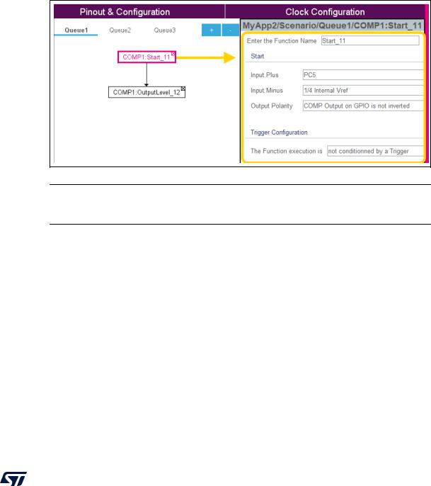
Once a function is chosen from the “LPBAM Function Toolbox” and added to a queue, it can be configured. In the center panel, click on a node to select it: the function is highlighted in pink, and its configuration is shown in the right panel (see Figure 422).
The example shows the “Start” parameters of the LPBAM COMP1_Start function. The HAL driver uses the same parameter names to configure a COMP IP. As mentioned before, the LPBAM firmware is not a HAL driver. However, the IP being unique, the LPBAM driver has been designed so that the IP parameters use, whenever possible, the same naming as found in the HAL driver.
Figure 422. LPBAM queue node configuration
Warning: LPBAM IP functions access IP hardware resources, to be properly configured in the “Pinout & Configuration” view.
When a parameter is set to a hardware resource such as a GPIO, the resource must be configured in the Pinout & Configuration view.
In the example shown in Figure 422, the COMP “Input Plus” is set to PC5. If PC5 is not configured in the “Pinout & configuration” view, the generated LPBAM application can gets a “null signal” on Input Plus, and will be not functional.
To fix this issue:
•Go to the Pinout&Configuration view
•Search PC5 using the search field
•Right-click the PC5 pin and select COMP_Inp (see Figure 423)
UM1718 Rev 41 |
377/453 |
Creating LPBAM projects |
UM1718 |
|
|
Figure 423. LPBAM node: configuring hardware resources
|
Another example can be made using a timer to generate a PWM signal. The HAL driver |
|
requires a timer channel to be configured as output. Same applies when using the LPBAM |
|
firmware. |
Note: |
All constraints concerning the initial configuration of the IP are mentioned in the LPBAM |
|
firmware documentation. Use STM32CubeMX “LPBAM Design check” mechanism (see |
|
dedicated section) to detect missing configurations. |
18.3.11 Node description: configuring a trigger
For all IPs and functions, with the LPBAM firmware it is possible to use a hardware signal to trigger a node. STM32CubeMX allows to configure such trigger from the node configuration panel. By default, the node execution is not triggered. When trigger is enabled, all possible trigger signals are listed.
Warning: It is the user responsibility to properly configure the triggers.
STM32CubeMX does not check for configuration errors.
Taking the COMP function “Start” as an example (see Figure 424), choose the function execution to be triggered on the rising edge of hardware signal, for the example, then, select the hardware signal among the list of hardware signals proposed.
378/453 |
UM1718 Rev 41 |

UM1718 |
Creating LPBAM projects |
|
|
Figure 424. LPBAM node trigger configuration
If a node is a function managing LPTIM1_CH1, it is possible to select LPTIM1_CH1 as the trigger (see Figure 425).
Figure 425. LPBAM node triggered using timer channel
18.3.12Node description: reconfiguring a DMA for Data transfer
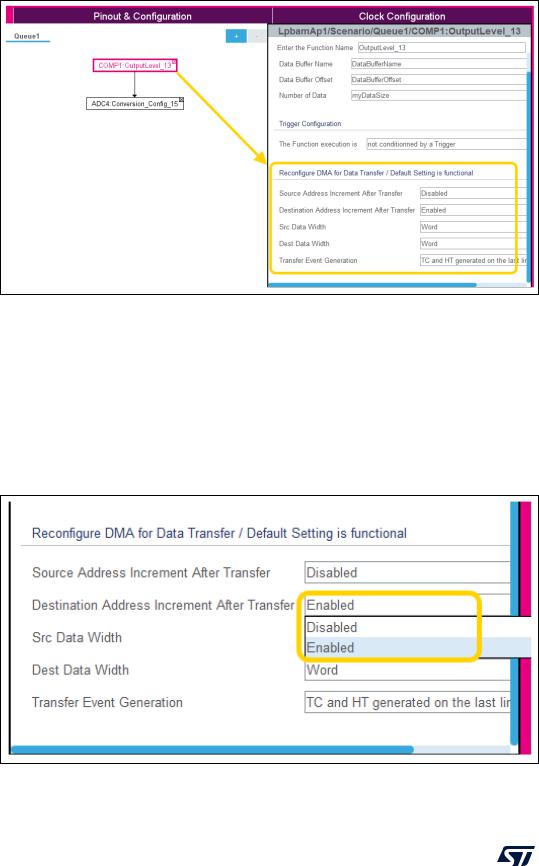
Nodes set to a function managing data transfers (all functions with associated data transfer and with a name not ending with _Config), come with a specific configuration section: “Reconfigure DMA for Data Transfer” (see Figure 426).
Each DMA data transfer is based on a specific configuration, including, among others, data size, buffer address, address increment. The DMA default settings are functional.
UM1718 Rev 41 |
379/453 |
Creating LPBAM projects |
UM1718 |
|
|
Figure 426. LPBAM node: reconfiguring a DMA
DMA settings can be changed, but they depend upon the IP and the function.
For example, for “COMP Output Level”:
•Data transferred are output data and are transferred from the register IP to the memory. The “Source Address” referring to the IP data register is not incremented: STM32CubeMX user interface shows that the “Source address increment after transfer” parameter cannot be enabled.
•Data transferred to memory can be saved at the same memory address, or in a Table: in this case, the “Destination Address increment after transfer” can be disabled or left enabled (see Figure 426).
Figure 427. Reconfiguring DMA for data transfer when destination is memory
380/453 |
UM1718 Rev 41 |