

STM32H745xI/G
Dual 32-bit Arm® Cortex®-M7 up to 480MHz and -M4 MCUs, up to 2MB Flash, 1MB RAM, 46 com. and analog interfaces, SMPS
Datasheet - production data
Features
Dual core
•32-bit Arm® Cortex®-M7 core with doubleprecision FPU and L1 cache: 16 Kbytes of data and 16 Kbytes of instruction cache; frequency up to 480 MHz, MPU, 1027 DMIPS/
2.14 DMIPS/MHz (Dhrystone 2.1), and DSP instructions
•32-bit Arm® 32-bit Cortex®-M4 core with FPU, Adaptive real-time accelerator (ART Accelerator™) for internal Flash memory and external memories, frequency up to 240 MHz, MPU, 300 DMIPS/1.25 DMIPS /MHz (Dhrystone 2.1), and DSP instructions
Memories
•Up to 2 Mbytes of Flash memory with read- while-write support
•1 Mbyte of RAM: 192 Kbytes of TCM RAM (inc. 64 Kbytes of ITCM RAM + 128 Kbytes of DTCM RAM for time critical routines),
864 Kbytes of user SRAM, and 4 Kbytes of SRAM in Backup domain
•Dual mode Quad-SPI memory interface running up to 133 MHz
•Flexible external memory controller with up to 32-bit data bus: SRAM, PSRAM, SDRAM/LPSDR SDRAM, NOR/NAND Flash memory clocked up to 125 MHz in Synchronous mode
•CRC calculation unit
FBGA |
FBGA |
|
|
|
|
|
|
LQFP144 |
|
UFBGA176+25 |
|||
TFBGA240+25 |
(10x10 mm) |
||||
(20x20 mm) |
|||||
(14x14 mm) |
|
|
|
||
LQFP176 |
|
|
|
||
|
|
|
|
||
(24x24 mm) |
|
|
|
|
|
LQFP208 |
|
|
|
|
|
(28x28 mm) |
|
|
|
|
|
Reset and power management
•3 separate power domains which can be independently clock-gated or switched off:
–D1: high-performance capabilities
–D2: communication peripherals and timers
–D3: reset/clock control/power management
•1.62 to 3.6 V application supply and I/Os
•POR, PDR, PVD and BOR
•Dedicated USB power embedding a 3.3 V internal regulator to supply the internal PHYs
•Embedded regulator (LDO) to supply the digital circuitry
•High power-efficiency SMPS step-down
converter regulator to directly supply VCORE and/or external circuitry
•Voltage scaling in Run and Stop mode (6 configurable ranges)
•Backup regulator (~0.9 V)
•Voltage reference for analog peripheral/VREF+
•1.2 to 3.6 V VBAT supply
•Low-power modes: Sleep, Stop, Standby and VBAT supporting battery charging
Security
• ROP, PC-ROP, active tamper
General-purpose input/outputs
• Up to 168 I/O ports with interrupt capability
Low-power consumption
•VBAT battery operating mode with charging capability
•CPU and domain power state monitoring pins
•2.95 µA in Standby mode (Backup SRAM OFF, RTC/LSE ON)
May 2019 |
DS12923 Rev 1 |
1/252 |
This is information on a product in full production. |
www.st.com |

STM32H745xI/G
Clock management
•Internal oscillators: 64 MHz HSI, 48 MHz HSI48, 4 MHz CSI, 32 kHz LSI
•External oscillators: 4-48 MHz HSE, 32.768 kHz LSE
•3× PLLs (1 for the system clock, 2 for kernel clocks) with Fractional mode
Interconnect matrix
•3 bus matrices (1 AXI and 2 AHB)
•Bridges (5× AHB2-APB, 2× AXI2-AHB)
4 DMA controllers to unload the CPU
•1× high-speed master direct memory access controller (MDMA) with linked list support
•2× dual-port DMAs with FIFO
•1× basic DMA with request router capabilities
Up to 35 communication peripherals
•4× I2Cs FM+ interfaces (SMBus/PMBus)
•4× USARTs/4x UARTs (ISO7816 interface, LIN, IrDA, up to 12.5 Mbit/s) and 1x LPUART
•6× SPIs, 3 with muxed duplex I2S audio class accuracy via internal audio PLL or external clock, 1x I2S in LP domain (up to 150 MHz)
•4x SAIs (serial audio interface)
•SPDIFRX interface
•SWPMI single-wire protocol master I/F
•MDIO Slave interface
•2× SD/SDIO/MMC interfaces (up to 125 MHz)
•2× CAN controllers: 2 with CAN FD, 1 with time-triggered CAN (TT-CAN)
•2× USB OTG interfaces (1FS, 1HS/FS) crystalless solution with LPM and BCD
•Ethernet MAC interface with DMA controller
•HDMI-CEC
•8- to 14-bit camera interface (up to 80 MHz)
11 analog peripherals
•3× ADCs with 16-bit max. resolution (up to 36 channels, up to 3.6 MSPS)
•1× temperature sensor
•2× 12-bit D/A converters (1 MHz)
•2× ultra-low-power comparators
•2× operational amplifiers (7.3 MHz bandwidth)
•1× digital filters for sigma delta modulator (DFSDM) with 8 channels/4 filters
Graphics
•LCD-TFT controller up to XGA resolution
•Chrom-ART graphical hardware Accelerator™ (DMA2D) to reduce CPU load
•Hardware JPEG Codec
Up to 22 timers and watchdogs
•1× high-resolution timer (2.1 ns max resolution)
•2× 32-bit timers with up to 4 IC/OC/PWM or pulse counter and quadrature (incremental) encoder input (up to 240 MHz)
•2× 16-bit advanced motor control timers (up to 240 MHz)
•10× 16-bit general-purpose timers (up to 240 MHz)
•5× 16-bit low-power timers (up to 240 MHz)
•4× watchdogs (independent and window)
•2× SysTick timers
•RTC with sub-second accuracy and hardware calendar
Debug mode
•SWD & JTAG interfaces
•4-Kbyte Embedded Trace Buffer
True random number generators (3 oscillators each)
96-bit unique ID
Optional support of extended temperature range up to 125 °C (specific part numbers)
All packages are ECOPACK®2 compliant
Table 1. Device summary
Reference |
Part number |
|
|
|
|
STM32H745xI |
STM32H745ZI, STM32H745II, |
|
STM32H745BI, STM32H745XI |
||
|
||
|
|
|
STM32H745xG |
STM32H745ZG, STM32H745IG, |
|
STM32H745BG, STM32H745XG |
||
|
|
2/252 |
DS12923 Rev 1 |

STM32H745xI/G |
Contents |
|
|
Contents
1 |
Introduction |
. . . . . . . . . . . . . . . . . . . . . . . . . . . . . . . . . . . . . . . . . . . . . . . |
13 |
|
2 |
Description . . |
. . . . . . . . . . . . . . . . . . . . . . . . . . . . . . . . . . . . . . . . . . . . . . |
14 |
|
3 |
Functional overview . . . . . . . . . . . . . . . . . . . . . . . . . . . . . . . . . . . . . . . . |
21 |
||
|
3.1 |
Dual Arm® Cortex® cores . . . . . . . . . . . . . . . . . . . . . . . . . . . . . . . . . . . . . |
21 |
|
|
|
3.1.1 |
Arm® Cortex®-M7 with FPU . . . . . . . . . . . . . . . . . . . . . . . . . . . . . . . . . . |
21 |
|
|
3.1.2 |
Arm® Cortex®-M4 with FPU . . . . . . . . . . . . . . . . . . . . . . . . . . . . . . . . . . |
22 |
3.2 Memory protection unit (MPU) . . . . . . . . . . . . . . . . . . . . . . . . . . . . . . . . . 22 3.3 Memories . . . . . . . . . . . . . . . . . . . . . . . . . . . . . . . . . . . . . . . . . . . . . . . . . 23
3.3.1 Embedded Flash memory . . . . . . . . . . . . . . . . . . . . . . . . . . . . . . . . . . . 23 3.3.2 Embedded SRAM . . . . . . . . . . . . . . . . . . . . . . . . . . . . . . . . . . . . . . . . . 23 3.3.3 ART™ accelerator . . . . . . . . . . . . . . . . . . . . . . . . . . . . . . . . . . . . . . . . . 24
3.4 Boot modes . . . . . . . . . . . . . . . . . . . . . . . . . . . . . . . . . . . . . . . . . . . . . . . 25 3.5 Power supply management . . . . . . . . . . . . . . . . . . . . . . . . . . . . . . . . . . . 26
3.5.1 Power supply scheme . . . . . . . . . . . . . . . . . . . . . . . . . . . . . . . . . . . . . . 26 3.5.2 Power supply supervisor . . . . . . . . . . . . . . . . . . . . . . . . . . . . . . . . . . . . 27 3.5.3 Voltage regulator (SMPS step-down converter and LDO) . . . . . . . . . . . 28 3.5.4 SMPS step-down converter . . . . . . . . . . . . . . . . . . . . . . . . . . . . . . . . . . 28
3.6 Low-power strategy . . . . . . . . . . . . . . . . . . . . . . . . . . . . . . . . . . . . . . . . . 29 3.7 Reset and clock controller (RCC) . . . . . . . . . . . . . . . . . . . . . . . . . . . . . . . 30
3.7.1 Clock management . . . . . . . . . . . . . . . . . . . . . . . . . . . . . . . . . . . . . . . . 30 3.7.2 System reset sources . . . . . . . . . . . . . . . . . . . . . . . . . . . . . . . . . . . . . . 31
3.8 General-purpose input/outputs (GPIOs) . . . . . . . . . . . . . . . . . . . . . . . . . . 31 3.9 Bus-interconnect matrix . . . . . . . . . . . . . . . . . . . . . . . . . . . . . . . . . . . . . . 31 3.10 DMA controllers . . . . . . . . . . . . . . . . . . . . . . . . . . . . . . . . . . . . . . . . . . . . 33 3.11 Chrom-ART Accelerator™ (DMA2D) . . . . . . . . . . . . . . . . . . . . . . . . . . . . 33 3.12 Nested vectored interrupt controller (NVIC) . . . . . . . . . . . . . . . . . . . . . . . 34 3.13 Extended interrupt and event controller (EXTI) . . . . . . . . . . . . . . . . . . . . 34 3.14 Cyclic redundancy check calculation unit (CRC) . . . . . . . . . . . . . . . . . . . 34 3.15 Flexible memory controller (FMC) . . . . . . . . . . . . . . . . . . . . . . . . . . . . . . 35 3.16 Quad-SPI memory interface (QUADSPI) . . . . . . . . . . . . . . . . . . . . . . . . . 35
DS12923 Rev 1 |
3/252 |

Contents |
STM32H745xI/G |
|
|
3.17 Analog-to-digital converters (ADCs) . . . . . . . . . . . . . . . . . . . . . . . . . . . . . 35 3.18 Temperature sensor . . . . . . . . . . . . . . . . . . . . . . . . . . . . . . . . . . . . . . . . . 36
3.19 VBAT operation . . . . . . . . . . . . . . . . . . . . . . . . . . . . . . . . . . . . . . . . . . . . . 36 3.20 Digital-to-analog converters (DAC) . . . . . . . . . . . . . . . . . . . . . . . . . . . . . 37
3.21 Ultra-low-power comparators (COMP) . . . . . . . . . . . . . . . . . . . . . . . . . . . 37 3.22 Operational amplifiers (OPAMP) . . . . . . . . . . . . . . . . . . . . . . . . . . . . . . . 37 3.23 Digital filter for sigma-delta modulators (DFSDM) . . . . . . . . . . . . . . . . . . 38 3.24 Digital camera interface (DCMI) . . . . . . . . . . . . . . . . . . . . . . . . . . . . . . . . 39 3.25 LCD-TFT controller . . . . . . . . . . . . . . . . . . . . . . . . . . . . . . . . . . . . . . . . . . 40 3.26 JPEG Codec (JPEG) . . . . . . . . . . . . . . . . . . . . . . . . . . . . . . . . . . . . . . . . 40 3.27 Random number generator (RNG) . . . . . . . . . . . . . . . . . . . . . . . . . . . . . . 40 3.28 Timers and watchdogs . . . . . . . . . . . . . . . . . . . . . . . . . . . . . . . . . . . . . . . 40
3.28.1 High-resolution timer (HRTIM1) . . . . . . . . . . . . . . . . . . . . . . . . . . . . . . . 42 3.28.2 Advanced-control timers (TIM1, TIM8) . . . . . . . . . . . . . . . . . . . . . . . . . 43 3.28.3 General-purpose timers (TIMx) . . . . . . . . . . . . . . . . . . . . . . . . . . . . . . . 43 3.28.4 Basic timers TIM6 and TIM7 . . . . . . . . . . . . . . . . . . . . . . . . . . . . . . . . . 44
3.28.5Low-power timers (LPTIM1, LPTIM2, LPTIM3, LPTIM4, LPTIM5) . . . . 44
3.28.6 Independent watchdogs . . . . . . . . . . . . . . . . . . . . . . . . . . . . . . . . . . . . . 44 3.28.7 Window watchdogs . . . . . . . . . . . . . . . . . . . . . . . . . . . . . . . . . . . . . . . . 44 3.28.8 SysTick timer . . . . . . . . . . . . . . . . . . . . . . . . . . . . . . . . . . . . . . . . . . . . . 44
3.29 Real-time clock (RTC), backup SRAM and backup registers . . . . . . . . . . 45 3.30 Inter-integrated circuit interface (I2C) . . . . . . . . . . . . . . . . . . . . . . . . . . . . 46
3.31Universal synchronous/asynchronous receiver transmitter (USART) . . . 46
3.32Low-power universal asynchronous receiver transmitter (LPUART) . . . . 47
3.33Serial peripheral interface (SPI)/interintegrated sound interfaces (I2S) . 48
3.34 Serial audio interfaces (SAI) . . . . . . . . . . . . . . . . . . . . . . . . . . . . . . . . . . . 48 3.35 SPDIFRX Receiver Interface (SPDIFRX) . . . . . . . . . . . . . . . . . . . . . . . . . 49 3.36 Single wire protocol master interface (SWPMI) . . . . . . . . . . . . . . . . . . . . 49 3.37 Management Data Input/Output (MDIO) slaves . . . . . . . . . . . . . . . . . . . . 50 3.38 SD/SDIO/MMC card host interfaces (SDMMC) . . . . . . . . . . . . . . . . . . . . 50 3.39 Controller area network (FDCAN1, FDCAN2) . . . . . . . . . . . . . . . . . . . . . 50 3.40 Universal serial bus on-the-go high-speed (OTG_HS) . . . . . . . . . . . . . . . 51 3.41 Ethernet MAC interface with dedicated DMA controller (ETH) . . . . . . . . . 51
4/252 |
DS12923 Rev 1 |

STM32H745xI/G |
|
Contents |
|
|
|
|
|
|
3.42 |
High-definition multimedia interface (HDMI) |
|
|
|
- consumer electronics control (CEC) . . . . . . . . . . . . . . . . . . . . . . |
. . . . . 52 |
|
3.43 |
Debug infrastructure . . . . . . . . . . . . . . . . . . . . . . . . . . . . . . . . . . . . |
. . . . . 52 |
4 |
Memory mapping . . . . . . . . . . . . . . . . . . . . . . . . . . . . . . . . . . . . . . . |
. . . . 54 |
|
5 |
Pin descriptions . . . . . . . . . . . . . . . . . . . . . . . . . . . . . . . . . . . . . . . |
. . . . 55 |
|
6 |
Electrical characteristics . . . . . . . . . . . . . . . . . . . . . . . . . . . . . . . . |
. . . 105 |
|
|
6.1 |
Parameter conditions . . . . . . . . . . . . . . . . . . . . . . . . . . . . . . . . . . . . |
. . . 105 |
6.1.1 Minimum and maximum values . . . . . . . . . . . . . . . . . . . . . . . . . . . . . . 105 6.1.2 Typical values . . . . . . . . . . . . . . . . . . . . . . . . . . . . . . . . . . . . . . . . . . . 105 6.1.3 Typical curves . . . . . . . . . . . . . . . . . . . . . . . . . . . . . . . . . . . . . . . . . . . 105 6.1.4 Loading capacitor . . . . . . . . . . . . . . . . . . . . . . . . . . . . . . . . . . . . . . . . 105 6.1.5 Pin input voltage . . . . . . . . . . . . . . . . . . . . . . . . . . . . . . . . . . . . . . . . . 105 6.1.6 Power supply scheme . . . . . . . . . . . . . . . . . . . . . . . . . . . . . . . . . . . . . 106 6.1.7 Current consumption measurement . . . . . . . . . . . . . . . . . . . . . . . . . . 107
6.2 Absolute maximum ratings . . . . . . . . . . . . . . . . . . . . . . . . . . . . . . . . . . . 107 6.3 Operating conditions . . . . . . . . . . . . . . . . . . . . . . . . . . . . . . . . . . . . . . . 109
6.3.1 General operating conditions . . . . . . . . . . . . . . . . . . . . . . . . . . . . . . . . 109 6.3.2 VCAP external capacitor . . . . . . . . . . . . . . . . . . . . . . . . . . . . . . . . . . . 112 6.3.3 SMPS step-down converter . . . . . . . . . . . . . . . . . . . . . . . . . . . . . . . . . 113 6.3.4 Operating conditions at power-up / power-down . . . . . . . . . . . . . . . . . 114 6.3.5 Embedded reset and power control block characteristics . . . . . . . . . . 115 6.3.6 Embedded reference voltage . . . . . . . . . . . . . . . . . . . . . . . . . . . . . . . . 116 6.3.7 Supply current characteristics . . . . . . . . . . . . . . . . . . . . . . . . . . . . . . . 117 6.3.8 Wakeup time from low-power modes . . . . . . . . . . . . . . . . . . . . . . . . . . 137 6.3.9 External clock source characteristics . . . . . . . . . . . . . . . . . . . . . . . . . . 138 6.3.10 Internal clock source characteristics . . . . . . . . . . . . . . . . . . . . . . . . . . 142 6.3.11 PLL characteristics . . . . . . . . . . . . . . . . . . . . . . . . . . . . . . . . . . . . . . . . 145 6.3.12 Memory characteristics . . . . . . . . . . . . . . . . . . . . . . . . . . . . . . . . . . . . 147 6.3.13 EMC characteristics . . . . . . . . . . . . . . . . . . . . . . . . . . . . . . . . . . . . . . . 148 6.3.14 Absolute maximum ratings (electrical sensitivity) . . . . . . . . . . . . . . . . 150 6.3.15 I/O current injection characteristics . . . . . . . . . . . . . . . . . . . . . . . . . . . 151 6.3.16 I/O port characteristics . . . . . . . . . . . . . . . . . . . . . . . . . . . . . . . . . . . . . 152 6.3.17 NRST pin characteristics . . . . . . . . . . . . . . . . . . . . . . . . . . . . . . . . . . . 159 6.3.18 FMC characteristics . . . . . . . . . . . . . . . . . . . . . . . . . . . . . . . . . . . . . . . 159
DS12923 Rev 1 |
5/252 |

Contents |
STM32H745xI/G |
|
|
6.3.19 Quad-SPI interface characteristics . . . . . . . . . . . . . . . . . . . . . . . . . . . 181 6.3.20 Delay block (DLYB) characteristics . . . . . . . . . . . . . . . . . . . . . . . . . . . 183 6.3.21 16-bit ADC characteristics . . . . . . . . . . . . . . . . . . . . . . . . . . . . . . . . . . 184 6.3.22 DAC characteristics . . . . . . . . . . . . . . . . . . . . . . . . . . . . . . . . . . . . . . . 193 6.3.23 Voltage reference buffer characteristics . . . . . . . . . . . . . . . . . . . . . . . 197 6.3.24 Temperature sensor characteristics . . . . . . . . . . . . . . . . . . . . . . . . . . . 198
6.3.25 Temperature and VBAT monitoring . . . . . . . . . . . . . . . . . . . . . . . . . . . . 199 6.3.26 Voltage booster for analog switch . . . . . . . . . . . . . . . . . . . . . . . . . . . . 199
6.3.27 Comparator characteristics . . . . . . . . . . . . . . . . . . . . . . . . . . . . . . . . . 200 6.3.28 Operational amplifier characteristics . . . . . . . . . . . . . . . . . . . . . . . . . . 201
6.3.29Digital filter for Sigma-Delta Modulators (DFSDM) characteristics . . . 203
6.3.30 Camera interface (DCMI) timing specifications . . . . . . . . . . . . . . . . . . 206 6.3.31 LCD-TFT controller (LTDC) characteristics . . . . . . . . . . . . . . . . . . . . . 207 6.3.32 Timer characteristics . . . . . . . . . . . . . . . . . . . . . . . . . . . . . . . . . . . . . . 209 6.3.33 Communication interfaces . . . . . . . . . . . . . . . . . . . . . . . . . . . . . . . . . . 209
7 |
Package information . . . . . . . . . . . . . . . . . . . . . . . . . . . . . . . . . . . . . . . |
229 |
|
|
7.1 |
LQFP144 package information . . . . . . . . . . . . . . . . . . . . . . . . . . . . . . . . |
230 |
|
7.2 |
LQFP176 package information . . . . . . . . . . . . . . . . . . . . . . . . . . . . . . . . |
234 |
|
7.3 |
LQFP208 package information . . . . . . . . . . . . . . . . . . . . . . . . . . . . . . . . |
238 |
|
7.4 |
UFBGA176+25 package information . . . . . . . . . . . . . . . . . . . . . . . . . . . |
242 |
|
7.5 |
TFBGA240+25 package information . . . . . . . . . . . . . . . . . . . . . . . . . . . |
245 |
|
7.6 |
Thermal characteristics . . . . . . . . . . . . . . . . . . . . . . . . . . . . . . . . . . . . . |
248 |
7.6.1 Reference document . . . . . . . . . . . . . . . . . . . . . . . . . . . . . . . . . . . . . . 249
8 |
Ordering information . . . . . . . . . . . . . . . . . . . . . . . . . . . . . . . . . . . . . . |
250 |
9 |
Revision history . . . . . . . . . . . . . . . . . . . . . . . . . . . . . . . . . . . . . . . . . . |
251 |
6/252 |
DS12923 Rev 1 |

STM32H745xI/G |
List of tables |
|
|
List of tables
Table 1. Device summary . . . . . . . . . . . . . . . . . . . . . . . . . . . . . . . . . . . . . . . . . . . . . . . . . . . . . . . . . . 2 Table 2. STM32H745xI/G features and peripheral counts . . . . . . . . . . . . . . . . . . . . . . . . . . . . . . . . 16 Table 3. System vs domain low-power mode . . . . . . . . . . . . . . . . . . . . . . . . . . . . . . . . . . . . . . . . . . 30 Table 4. DFSDM implementation . . . . . . . . . . . . . . . . . . . . . . . . . . . . . . . . . . . . . . . . . . . . . . . . . . . 39 Table 5. Timer feature comparison. . . . . . . . . . . . . . . . . . . . . . . . . . . . . . . . . . . . . . . . . . . . . . . . . . 41 Table 6. USART features . . . . . . . . . . . . . . . . . . . . . . . . . . . . . . . . . . . . . . . . . . . . . . . . . . . . . . . . . 47 Table 7. Legend/abbreviations used in the pinout table . . . . . . . . . . . . . . . . . . . . . . . . . . . . . . . . . . 60 Table 8. STM32H745xI/G pin/ball definition . . . . . . . . . . . . . . . . . . . . . . . . . . . . . . . . . . . . . . . . . . . 61 Table 9. Port A alternate functions . . . . . . . . . . . . . . . . . . . . . . . . . . . . . . . . . . . . . . . . . . . . . . . . . . 88 Table 10. Port B alternate functions . . . . . . . . . . . . . . . . . . . . . . . . . . . . . . . . . . . . . . . . . . . . . . . . . . 90 Table 11. Port C alternate functions . . . . . . . . . . . . . . . . . . . . . . . . . . . . . . . . . . . . . . . . . . . . . . . . . . 92 Table 12. Port D alternate functions . . . . . . . . . . . . . . . . . . . . . . . . . . . . . . . . . . . . . . . . . . . . . . . . . . 94 Table 13. Port E alternate functions . . . . . . . . . . . . . . . . . . . . . . . . . . . . . . . . . . . . . . . . . . . . . . . . . . 96 Table 14. Port F alternate functions . . . . . . . . . . . . . . . . . . . . . . . . . . . . . . . . . . . . . . . . . . . . . . . . . . 98 Table 15. Port G alternate functions . . . . . . . . . . . . . . . . . . . . . . . . . . . . . . . . . . . . . . . . . . . . . . . . . . 99 Table 16. Port H alternate functions . . . . . . . . . . . . . . . . . . . . . . . . . . . . . . . . . . . . . . . . . . . . . . . . . 101 Table 17. Port I alternate functions. . . . . . . . . . . . . . . . . . . . . . . . . . . . . . . . . . . . . . . . . . . . . . . . . . 102 Table 18. Port J alternate functions . . . . . . . . . . . . . . . . . . . . . . . . . . . . . . . . . . . . . . . . . . . . . . . . . 103 Table 19. Port K alternate functions . . . . . . . . . . . . . . . . . . . . . . . . . . . . . . . . . . . . . . . . . . . . . . . . . 104 Table 20. Voltage characteristics . . . . . . . . . . . . . . . . . . . . . . . . . . . . . . . . . . . . . . . . . . . . . . . . . . . 107 Table 21. Current characteristics . . . . . . . . . . . . . . . . . . . . . . . . . . . . . . . . . . . . . . . . . . . . . . . . . . . 108 Table 22. Thermal characteristics. . . . . . . . . . . . . . . . . . . . . . . . . . . . . . . . . . . . . . . . . . . . . . . . . . . 108 Table 23. General operating conditions . . . . . . . . . . . . . . . . . . . . . . . . . . . . . . . . . . . . . . . . . . . . . . 109 Table 24. Supply voltage and maximum frequency configuration . . . . . . . . . . . . . . . . . . . . . . . . . . 111 Table 25. VCAP operating conditions. . . . . . . . . . . . . . . . . . . . . . . . . . . . . . . . . . . . . . . . . . . . . . . . 112 Table 26. Characteristics of SMPS step-down converter external components. . . . . . . . . . . . . . . . 113 Table 27. SMPS step-down converter characteristics for external usage . . . . . . . . . . . . . . . . . . . . 114 Table 28. Operating conditions at power-up / power-down (regulator ON) . . . . . . . . . . . . . . . . . . . 114 Table 29. Reset and power control block characteristics . . . . . . . . . . . . . . . . . . . . . . . . . . . . . . . . . 115 Table 30. Embedded reference voltage . . . . . . . . . . . . . . . . . . . . . . . . . . . . . . . . . . . . . . . . . . . . . . 116 Table 31. Internal reference voltage calibration values . . . . . . . . . . . . . . . . . . . . . . . . . . . . . . . . . . 117 Table 32. Typical and maximum current consumption in Run mode, code with data processing
running from ITCM for Cortex-M7 core, and Flash memory for Cortex-M4
(ART accelerator ON), LDO regulator ON . . . . . . . . . . . . . . . . . . . . . . . . . . . . . . . . . . . . 118 Table 33. Typical and maximum current consumption in Run mode, code with data processing
running from ITCM for Arm Cortex-M7 and Flash memory for Arm Cortex-M4,
ART accelerator ON, SMPS regulator . . . . . . . . . . . . . . . . . . . . . . . . . . . . . . . . . . . . . . . 118 Table 34. Typical and maximum current consumption in Run mode, code with data processing
running from Flash memory, both cores running, cache ON,
ART accelerator ON, LDO regulator ON . . . . . . . . . . . . . . . . . . . . . . . . . . . . . . . . . . . . . 119 Table 35. Typical and maximum current consumption in Run mode, code with data processing
running from Flash memory, both cores running, cache OFF,
ART accelerator OFF, LDO regulator ON. . . . . . . . . . . . . . . . . . . . . . . . . . . . . . . . . . . . . 119 Table 36. Typical and maximum current consumption in Run mode, code with data processing
running from ITCM, only Arm Cortex-M7 running, LDO regulator ON . . . . . . . . . . . . . . . 120 Table 37. Typical and maximum current consumption in Run mode, code with data processing
running from ITCM, only Arm Cortex-M7 running, SMPS regulator. . . . . . . . . . . . . . . . . 121 Table 38. Typical and maximum current consumption in Run mode, code with data processing
DS12923 Rev 1 |
7/252 |

List of tables |
STM32H745xI/G |
|
|
running from Flash memory, only Arm Cortex-M7 running, cache ON,
LDO regulator ON. . . . . . . . . . . . . . . . . . . . . . . . . . . . . . . . . . . . . . . . . . . . . . . . . . . . . . . 121 Table 39. Typical and maximum current consumption in Run mode, code with data processing
running from Flash memory, only Arm Cortex-M7 running, cache OFF,
LDO regulator ON. . . . . . . . . . . . . . . . . . . . . . . . . . . . . . . . . . . . . . . . . . . . . . . . . . . . . . . 122 Table 40. Typical and maximum current consumption batch acquisition mode,
LDO regulator ON. . . . . . . . . . . . . . . . . . . . . . . . . . . . . . . . . . . . . . . . . . . . . . . . . . . . . . . 122 Table 41. Typical and maximum current consumption in Run mode, code with data processing
running from Flash memory, only Arm Cortex-M4 running, ART accelerator ON,
LDO regulator ON. . . . . . . . . . . . . . . . . . . . . . . . . . . . . . . . . . . . . . . . . . . . . . . . . . . . . . . 123 Table 42. Typical and maximum current consumption in Run mode, code with data processing
running from Flash bank 2, only Arm Cortex-M4 running, ART accelerator ON,
SMPS regulator . . . . . . . . . . . . . . . . . . . . . . . . . . . . . . . . . . . . . . . . . . . . . . . . . . . . . . . . 123 Table 43. Typical and maximum current consumption in Stop, LDO regulator ON . . . . . . . . . . . . . 124 Table 44. Typical and maximum current consumption in Stop, SMPS regulator . . . . . . . . . . . . . . . 125 Table 45. Typical and maximum current consumption in Sleep mode, LDO regulator ON . . . . . . . 126 Table 46. Typical and maximum current consumption in Sleep mode, SMPS regulator . . . . . . . . . 126 Table 47. Typical and maximum current consumption in Standby . . . . . . . . . . . . . . . . . . . . . . . . . . 127 Table 48. Typical and maximum current consumption in VBAT mode . . . . . . . . . . . . . . . . . . . . . . . 127 Table 49. Peripheral current consumption in Run mode . . . . . . . . . . . . . . . . . . . . . . . . . . . . . . . . . 132 Table 50. Low-power mode wakeup timings . . . . . . . . . . . . . . . . . . . . . . . . . . . . . . . . . . . . . . . . . . 137 Table 51. High-speed external user clock characteristics. . . . . . . . . . . . . . . . . . . . . . . . . . . . . . . . . 138 Table 52. Low-speed external user clock characteristics . . . . . . . . . . . . . . . . . . . . . . . . . . . . . . . . . 139 Table 53. 4-48 MHz HSE oscillator characteristics . . . . . . . . . . . . . . . . . . . . . . . . . . . . . . . . . . . . . 140 Table 54. Low-speed external user clock characteristics . . . . . . . . . . . . . . . . . . . . . . . . . . . . . . . . . 141 Table 55. HSI48 oscillator characteristics. . . . . . . . . . . . . . . . . . . . . . . . . . . . . . . . . . . . . . . . . . . . . 142 Table 56. HSI oscillator characteristics. . . . . . . . . . . . . . . . . . . . . . . . . . . . . . . . . . . . . . . . . . . . . . . 143 Table 57. CSI oscillator characteristics. . . . . . . . . . . . . . . . . . . . . . . . . . . . . . . . . . . . . . . . . . . . . . . 143 Table 58. LSI oscillator characteristics . . . . . . . . . . . . . . . . . . . . . . . . . . . . . . . . . . . . . . . . . . . . . . . 144 Table 59. PLL characteristics (wide VCO frequency range). . . . . . . . . . . . . . . . . . . . . . . . . . . . . . . 145 Table 60. PLL characteristics (medium VCO frequency range) . . . . . . . . . . . . . . . . . . . . . . . . . . . . 146 Table 61. Flash memory characteristics . . . . . . . . . . . . . . . . . . . . . . . . . . . . . . . . . . . . . . . . . . . . . . 147 Table 62. Flash memory programming (single bank configuration nDBANK=1) . . . . . . . . . . . . . . . 147 Table 63. Flash memory endurance and data retention . . . . . . . . . . . . . . . . . . . . . . . . . . . . . . . . . . 148 Table 64. EMS characteristics . . . . . . . . . . . . . . . . . . . . . . . . . . . . . . . . . . . . . . . . . . . . . . . . . . . . . 148 Table 65. EMI characteristics . . . . . . . . . . . . . . . . . . . . . . . . . . . . . . . . . . . . . . . . . . . . . . . . . . . . . . 149 Table 66. ESD absolute maximum ratings . . . . . . . . . . . . . . . . . . . . . . . . . . . . . . . . . . . . . . . . . . . . 150 Table 67. Electrical sensitivities . . . . . . . . . . . . . . . . . . . . . . . . . . . . . . . . . . . . . . . . . . . . . . . . . . . . 150 Table 68. I/O current injection susceptibility . . . . . . . . . . . . . . . . . . . . . . . . . . . . . . . . . . . . . . . . . . . 151 Table 69. I/O static characteristics . . . . . . . . . . . . . . . . . . . . . . . . . . . . . . . . . . . . . . . . . . . . . . . . . . 152 Table 70. Output voltage characteristics for all I/Os except PC13, PC14, PC15 and PI8 . . . . . . . . 154 Table 71. Output voltage characteristics for PC13, PC14, PC15 and PI8 . . . . . . . . . . . . . . . . . . . . 155 Table 72. Output timing characteristics (HSLV OFF) . . . . . . . . . . . . . . . . . . . . . . . . . . . . . . . . . . . . 156 Table 73. Output timing characteristics (HSLV ON) . . . . . . . . . . . . . . . . . . . . . . . . . . . . . . . . . . . . . 158 Table 74. NRST pin characteristics . . . . . . . . . . . . . . . . . . . . . . . . . . . . . . . . . . . . . . . . . . . . . . . . . 159 Table 75. Asynchronous non-multiplexed SRAM/PSRAM/NOR read timings . . . . . . . . . . . . . . . . . 161 Table 76. Asynchronous non-multiplexed SRAM/PSRAM/NOR read-NWAIT timings . . . . . . . . . . . 161 Table 77. Asynchronous non-multiplexed SRAM/PSRAM/NOR write timings . . . . . . . . . . . . . . . . . 163 Table 78. Asynchronous non-multiplexed SRAM/PSRAM/NOR write-NWAIT timings. . . . . . . . . . . 163 Table 79. Asynchronous multiplexed PSRAM/NOR read timings. . . . . . . . . . . . . . . . . . . . . . . . . . . 165 Table 80. Asynchronous multiplexed PSRAM/NOR read-NWAIT timings . . . . . . . . . . . . . . . . . . . . 165 Table 81. Asynchronous multiplexed PSRAM/NOR write timings . . . . . . . . . . . . . . . . . . . . . . . . . . 166
8/252 |
DS12923 Rev 1 |

STM32H745xI/G |
List of tables |
|
|
Table 82. Asynchronous multiplexed PSRAM/NOR write-NWAIT timings . . . . . . . . . . . . . . . . . . . . 166 Table 83. Synchronous multiplexed NOR/PSRAM read timings . . . . . . . . . . . . . . . . . . . . . . . . . . . 168 Table 84. Synchronous multiplexed PSRAM write timings. . . . . . . . . . . . . . . . . . . . . . . . . . . . . . . . 170 Table 85. Synchronous non-multiplexed NOR/PSRAM read timings . . . . . . . . . . . . . . . . . . . . . . . . 172 Table 86. Synchronous non-multiplexed PSRAM write timings . . . . . . . . . . . . . . . . . . . . . . . . . . . . 174 Table 87. Switching characteristics for NAND Flash read cycles . . . . . . . . . . . . . . . . . . . . . . . . . . . 177 Table 88. Switching characteristics for NAND Flash write cycles. . . . . . . . . . . . . . . . . . . . . . . . . . . 177 Table 89. SDRAM read timings . . . . . . . . . . . . . . . . . . . . . . . . . . . . . . . . . . . . . . . . . . . . . . . . . . . . 179 Table 90. LPSDR SDRAM read timings . . . . . . . . . . . . . . . . . . . . . . . . . . . . . . . . . . . . . . . . . . . . . . 179 Table 91. SDRAM Write timings . . . . . . . . . . . . . . . . . . . . . . . . . . . . . . . . . . . . . . . . . . . . . . . . . . . . 180 Table 92. LPSDR SDRAM Write timings . . . . . . . . . . . . . . . . . . . . . . . . . . . . . . . . . . . . . . . . . . . . . 181 Table 93. QUADSPI characteristics in SDR mode . . . . . . . . . . . . . . . . . . . . . . . . . . . . . . . . . . . . . . 181 Table 94. QUADSPI characteristics in DDR mode . . . . . . . . . . . . . . . . . . . . . . . . . . . . . . . . . . . . . . 182 Table 95. Delay Block characteristics. . . . . . . . . . . . . . . . . . . . . . . . . . . . . . . . . . . . . . . . . . . . . . . . 183 Table 96. ADC characteristics . . . . . . . . . . . . . . . . . . . . . . . . . . . . . . . . . . . . . . . . . . . . . . . . . . . . . 184 Table 97. Minimum sampling time vs RAIN . . . . . . . . . . . . . . . . . . . . . . . . . . . . . . . . . . . . . . . . . . . 188 Table 98. ADC accuracy. . . . . . . . . . . . . . . . . . . . . . . . . . . . . . . . . . . . . . . . . . . . . . . . . . . . . . . . . . 190 Table 99. DAC characteristics . . . . . . . . . . . . . . . . . . . . . . . . . . . . . . . . . . . . . . . . . . . . . . . . . . . . . 193 Table 100. DAC accuracy. . . . . . . . . . . . . . . . . . . . . . . . . . . . . . . . . . . . . . . . . . . . . . . . . . . . . . . . . . 195 Table 101. VREFBUF characteristics . . . . . . . . . . . . . . . . . . . . . . . . . . . . . . . . . . . . . . . . . . . . . . . . . 197 Table 102. Temperature sensor characteristics . . . . . . . . . . . . . . . . . . . . . . . . . . . . . . . . . . . . . . . . . 198 Table 103. Temperature sensor calibration values. . . . . . . . . . . . . . . . . . . . . . . . . . . . . . . . . . . . . . . 198
Table 104. VBAT monitoring characteristics . . . . . . . . . . . . . . . . . . . . . . . . . . . . . . . . . . . . . . . . . . . . 199 Table 105. VBAT charging characteristics . . . . . . . . . . . . . . . . . . . . . . . . . . . . . . . . . . . . . . . . . . . . . . 199 Table 106. Temperature monitoring characteristics . . . . . . . . . . . . . . . . . . . . . . . . . . . . . . . . . . . . . . 199
Table 107. Voltage booster for analog switch characteristics. . . . . . . . . . . . . . . . . . . . . . . . . . . . . . . 199 Table 108. COMP characteristics . . . . . . . . . . . . . . . . . . . . . . . . . . . . . . . . . . . . . . . . . . . . . . . . . . . . 200 Table 109. Operational amplifier characteristics. . . . . . . . . . . . . . . . . . . . . . . . . . . . . . . . . . . . . . . . . 201 Table 110. DFSDM measured timing 1.62-3.6 V . . . . . . . . . . . . . . . . . . . . . . . . . . . . . . . . . . . . . . . . 204 Table 111. DCMI characteristics. . . . . . . . . . . . . . . . . . . . . . . . . . . . . . . . . . . . . . . . . . . . . . . . . . . . . 206 Table 112. LTDC characteristics . . . . . . . . . . . . . . . . . . . . . . . . . . . . . . . . . . . . . . . . . . . . . . . . . . . . 207 Table 113. TIMx characteristics . . . . . . . . . . . . . . . . . . . . . . . . . . . . . . . . . . . . . . . . . . . . . . . . . . . . . 209 Table 114. Minimum i2c_ker_ck frequency in all I2C modes . . . . . . . . . . . . . . . . . . . . . . . . . . . . . . . 210 Table 115. I2C analog filter characteristics. . . . . . . . . . . . . . . . . . . . . . . . . . . . . . . . . . . . . . . . . . . . . 210 Table 116. USART characteristics . . . . . . . . . . . . . . . . . . . . . . . . . . . . . . . . . . . . . . . . . . . . . . . . . . . 211
Table 117. SPI characteristics . . . . . . . . . . . . . . . . . . . . . . . . . . . . . . . . . . . . . . . . . . . . . . . . . . . . . . 213 Table 118. I2S dynamic characteristics . . . . . . . . . . . . . . . . . . . . . . . . . . . . . . . . . . . . . . . . . . . . . . . 216
Table 119. SAI characteristics . . . . . . . . . . . . . . . . . . . . . . . . . . . . . . . . . . . . . . . . . . . . . . . . . . . . . . 218 Table 120. MDIO Slave timing parameters. . . . . . . . . . . . . . . . . . . . . . . . . . . . . . . . . . . . . . . . . . . . . 220 Table 121. Dynamics characteristics: SD / MMC characteristics, VDD=2.7 to 3.6 V . . . . . . . . . . . . . 221 Table 122. Dynamics characteristics: eMMC characteristics VDD=1.71V to 1.9V . . . . . . . . . . . . . . . 222 Table 123. Dynamics characteristics: USB ULPI . . . . . . . . . . . . . . . . . . . . . . . . . . . . . . . . . . . . . . . . 224 Table 124. Dynamics characteristics: Ethernet MAC signals for SMI . . . . . . . . . . . . . . . . . . . . . . . . 225 Table 125. Dynamics characteristics: Ethernet MAC signals for RMII . . . . . . . . . . . . . . . . . . . . . . . . 226 Table 126. Dynamics characteristics: Ethernet MAC signals for MII . . . . . . . . . . . . . . . . . . . . . . . . . 226 Table 127. Dynamics JTAG characteristics . . . . . . . . . . . . . . . . . . . . . . . . . . . . . . . . . . . . . . . . . . . . 227 Table 128. Dynamics SWD characteristics: . . . . . . . . . . . . . . . . . . . . . . . . . . . . . . . . . . . . . . . . . . . . 228 Table 129. LQFP144 package mechanical data. . . . . . . . . . . . . . . . . . . . . . . . . . . . . . . . . . . . . . . . . 231 Table 130. LQFP176 package mechanical data. . . . . . . . . . . . . . . . . . . . . . . . . . . . . . . . . . . . . . . . . 234 Table 131. LQFP208 package mechanical data. . . . . . . . . . . . . . . . . . . . . . . . . . . . . . . . . . . . . . . . . 239 Table 132. UFBGA176+25 package mechanical data . . . . . . . . . . . . . . . . . . . . . . . . . . . . . . . . . . . . 242 Table 133. UFBGA176+25 recommended PCB design rules (0.65 mm pitch BGA) . . . . . . . . . . . . . 243
DS12923 Rev 1 |
9/252 |

List of tables |
STM32H745xI/G |
|
|
Table 134. TFBG240+25 ball package mechanical data . . . . . . . . . . . . . . . . . . . . . . . . . . . . . . . . . . 246 Table 135. TFBGA240+25 recommended PCB design rules (0.8 mm pitch) . . . . . . . . . . . . . . . . . . . 247 Table 136. Thermal characteristics. . . . . . . . . . . . . . . . . . . . . . . . . . . . . . . . . . . . . . . . . . . . . . . . . . . 248 Table 137. Document revision history . . . . . . . . . . . . . . . . . . . . . . . . . . . . . . . . . . . . . . . . . . . . . . . . 251
10/252 |
DS12923 Rev 1 |
STM32H745xI/G |
List of figures |
|
|
List of figures
Figure 1. |
STM32H745xI/G block diagram . . . . . . . . . . . . . . . . . . . . . . . . . . . . . . . . . . . . . . . . |
. . . . 19 |
Figure 2. |
TFBGA240+25 ball assignment differences . . . . . . . . . . . . . . . . . . . . . . . . . . . . . . . |
. . . . 20 |
Figure 3. ART™ accelerator schematic and environment . . . . . . . . . . . . . . . . . . . . . . . . . . . . . |
. . . . 25 |
|
Figure 4. |
Power-up/power-down sequence . . . . . . . . . . . . . . . . . . . . . . . . . . . . . . . . . . . . . . . . |
. . . . 27 |
Figure 5. |
STM32H745xI/G bus matrix . . . . . . . . . . . . . . . . . . . . . . . . . . . . . . . . . . . . . . . . . . . |
. . . . 32 |
Figure 6. |
LQFP144 pinout . . . . . . . . . . . . . . . . . . . . . . . . . . . . . . . . . . . . . . . . . . . . . . . . . . . . . |
. . . . 55 |
Figure 7. |
LQFP176 pinout . . . . . . . . . . . . . . . . . . . . . . . . . . . . . . . . . . . . . . . . . . . . . . . . . . . . . |
. . . . 56 |
Figure 8. |
UFBGA176+25 ballout . . . . . . . . . . . . . . . . . . . . . . . . . . . . . . . . . . . . . . . . . . . . . . . . |
. . . . 57 |
Figure 9. |
LQFP208 pinout . . . . . . . . . . . . . . . . . . . . . . . . . . . . . . . . . . . . . . . . . . . . . . . . . . . . |
. . . . 58 |
Figure 10. |
TFBGA240+25 ballout . . . . . . . . . . . . . . . . . . . . . . . . . . . . . . . . . . . . . . . . . . . . . . . |
. . . . 59 |
Figure 11. |
Pin loading conditions. . . . . . . . . . . . . . . . . . . . . . . . . . . . . . . . . . . . . . . . . . . . . . . . . |
. . . 105 |
Figure 12. |
Pin input voltage . . . . . . . . . . . . . . . . . . . . . . . . . . . . . . . . . . . . . . . . . . . . . . . . . . . . . |
. . . 105 |
Figure 13. |
Power supply scheme . . . . . . . . . . . . . . . . . . . . . . . . . . . . . . . . . . . . . . . . . . . . . . . . |
. . . 106 |
Figure 14. |
Current consumption measurement scheme . . . . . . . . . . . . . . . . . . . . . . . . . . . . . . . |
. . . 107 |
Figure 15. |
External capacitor CEXT . . . . . . . . . . . . . . . . . . . . . . . . . . . . . . . . . . . . . . . . . . . . . . . |
. . . 112 |
Figure 16. |
External components for SMPS step-down converter . . . . . . . . . . . . . . . . . . . . . . . . |
. . . 113 |
Figure 17. |
Typical SMPS efficiency (%) vs load current (A) in Run mode at TJ = 30 °C. . . . . . . |
. . . 128 |
Figure 18. |
Typical SMPS efficiency (%) vs load current (A) in Run mode at TJ = TJmax . . . . . |
. . . 128 |
Figure 19. |
Typical SMPS efficiency (%) vs load current (A) in low-power mode at TJ = 30 °C . . |
. . . 129 |
Figure 20. |
Typical SMPS efficiency (%) vs load current (A) in low-power mode at TJ = TJmax |
. . . 130 |
Figure 21. |
High-speed external clock source AC timing diagram . . . . . . . . . . . . . . . . . . . . . . . . |
. . . 138 |
Figure 22. |
Low-speed external clock source AC timing diagram. . . . . . . . . . . . . . . . . . . . . . . . . |
. . . 139 |
Figure 23. |
Typical application with an 8 MHz crystal . . . . . . . . . . . . . . . . . . . . . . . . . . . . . . . . . . |
. . . 141 |
Figure 24. |
Typical application with a 32.768 kHz crystal . . . . . . . . . . . . . . . . . . . . . . . . . . . . . . . |
. . . 142 |
Figure 25. |
VIL/VIH for all I/Os except BOOT0 . . . . . . . . . . . . . . . . . . . . . . . . . . . . . . . . . . . . . . . |
. . . 153 |
Figure 26. |
Recommended NRST pin protection . . . . . . . . . . . . . . . . . . . . . . . . . . . . . . . . . . . . . |
. . . 159 |
Figure 27. |
Asynchronous non-multiplexed SRAM/PSRAM/NOR read waveforms . . . . . . . . . . . |
. . . 160 |
Figure 28. |
Asynchronous non-multiplexed SRAM/PSRAM/NOR write waveforms . . . . . . . . . . . |
. . . 162 |
Figure 29. |
Asynchronous multiplexed PSRAM/NOR read waveforms. . . . . . . . . . . . . . . . . . . . . |
. . . 164 |
Figure 30. |
Synchronous multiplexed NOR/PSRAM read timings . . . . . . . . . . . . . . . . . . . . . . . . |
. . . 167 |
Figure 31. |
Synchronous multiplexed PSRAM write timings. . . . . . . . . . . . . . . . . . . . . . . . . . . . . |
. . . 169 |
Figure 32. |
Synchronous non-multiplexed NOR/PSRAM read timings . . . . . . . . . . . . . . . . . . . . . |
. . . 171 |
Figure 33. |
Synchronous non-multiplexed PSRAM write timings . . . . . . . . . . . . . . . . . . . . . . . . . |
. . . 173 |
Figure 34. |
NAND controller waveforms for read access . . . . . . . . . . . . . . . . . . . . . . . . . . . . . . . |
. . . 175 |
Figure 35. |
NAND controller waveforms for write access . . . . . . . . . . . . . . . . . . . . . . . . . . . . . . . |
. . . 176 |
Figure 36. |
NAND controller waveforms for common memory read access . . . . . . . . . . . . . . . . . |
. . . 176 |
Figure 37. |
NAND controller waveforms for common memory write access. . . . . . . . . . . . . . . . . |
. . . 177 |
Figure 38. |
SDRAM read access waveforms (CL = 1) . . . . . . . . . . . . . . . . . . . . . . . . . . . . . . . . . |
. . . 178 |
Figure 39. |
SDRAM write access waveforms . . . . . . . . . . . . . . . . . . . . . . . . . . . . . . . . . . . . . . . . |
. . . 180 |
Figure 40. |
Quad-SPI timing diagram - SDR mode. . . . . . . . . . . . . . . . . . . . . . . . . . . . . . . . . . . . |
. . . 183 |
Figure 41. |
Quad-SPI timing diagram - DDR mode . . . . . . . . . . . . . . . . . . . . . . . . . . . . . . . . . . . |
. . . 183 |
Figure 42. |
ADC accuracy characteristics (12-bit resolution) . . . . . . . . . . . . . . . . . . . . . . . . . . . . |
. . . 191 |
Figure 43. |
Typical connection diagram using the ADC . . . . . . . . . . . . . . . . . . . . . . . . . . . . . . . . |
. . . 191 |
Figure 44. |
Power supply and reference decoupling (VREF+ not connected to VDDA). . . . . . . . . . |
. . . 192 |
Figure 45. |
Power supply and reference decoupling (VREF+ connected to VDDA). . . . . . . . . . . . . |
. . . 192 |
Figure 46. |
12-bit buffered /non-buffered DAC . . . . . . . . . . . . . . . . . . . . . . . . . . . . . . . . . . . . . . . |
. . . 196 |
Figure 47. |
Channel transceiver timing diagrams . . . . . . . . . . . . . . . . . . . . . . . . . . . . . . . . . . . . . |
. . . 205 |
Figure 48. |
DCMI timing diagram . . . . . . . . . . . . . . . . . . . . . . . . . . . . . . . . . . . . . . . . . . . . . . . . . |
. . . 206 |
DS12923 Rev 1 |
11/252 |

List of figures |
STM32H745xI/G |
|
Figure 49. LCD-TFT horizontal timing diagram . . . . . . . . . . . . . . . . . . . . . . . . . . . . . . . |
. . . . . . . . . . 208 |
|
Figure 50. LCD-TFT vertical timing diagram . . . . . . . . . . . . . . . . . . . . . . . . . . . . . . . . . |
. . . . . . . . . . 208 |
|
Figure 51. USART timing diagram in Master mode . . . . . . . . . . . . . . . . . . . . . . . . . . . . |
. . . . . . . . . . 212 |
|
Figure 52. USART timing diagram in Slave mode . . . . . . . . . . . . . . . . . . . . . . . . . . . . |
. . . . . . . . . . 212 |
|
Figure 53. SPI timing diagram - slave mode and CPHA = 0 . . . . . . . . . . . . . . . . . . . . . |
. . . . . . . . . . 214 |
|
Figure 54. SPI timing diagram - slave mode and CPHA = 1(1) . . . . . . . . . . . . . . . . . . . |
. . . . . . . . . . 215 |
|
Figure 55. SPI timing diagram - master mode(1) . . . . . . . . . . . . . . . . . . . . . . . . . . . . . . |
. . . . . . . . . . 215 |
|
Figure 56. I2S slave timing diagram (Philips protocol)(1) . . . . . . . . . . . . . . . . . . . . . . . . |
. . . . . . . . . . 217 |
|
Figure 57. I2S master timing diagram (Philips protocol)(1) . . . . . . . . . . . . . . . . . . . . . . . |
. . . . . . . . . . 217 |
|
Figure 58. SAI master timing waveforms . . . . . . . . . . . . . . . . . . . . . . . . . . . . . . . . . . . . |
. . . . . . . . . . 220 |
|
Figure 59. SAI slave timing waveforms . . . . . . . . . . . . . . . . . . . . . . . . . . . . . . . . . . . . . |
. . . . . . . . . . 220 |
|
Figure 60. MDIO Slave timing diagram . . . . . . . . . . . . . . . . . . . . . . . . . . . . . . . . . . . . . |
. . . . . . . . . . 221 |
|
Figure 61. SDIO high-speed mode . . . . . . . . . . . . . . . . . . . . . . . . . . . . . . . . . . . . . . . . |
. . . . . . . . . . 223 |
|
Figure 62. SD default mode . . . . . . . . . . . . . . . . . . . . . . . . . . . . . . . . . . . . . . . . . . . . . . |
. . . . . . . . . . 223 |
|
Figure 63. |
DDR mode . . . . . . . . . . . . . . . . . . . . . . . . . . . . . . . . . . . . . . . . . . . . . . . . . . |
. . . . . . . . . . 223 |
Figure 64. ULPI timing diagram . . . . . . . . . . . . . . . . . . . . . . . . . . . . . . . . . . . . . . . . . . . |
. . . . . . . . . . 224 |
|
Figure 65. Ethernet SMI timing diagram . . . . . . . . . . . . . . . . . . . . . . . . . . . . . . . . . . . . |
. . . . . . . . . . 225 |
|
Figure 66. Ethernet RMII timing diagram . . . . . . . . . . . . . . . . . . . . . . . . . . . . . . . . . . . . |
. . . . . . . . . . 226 |
|
Figure 67. Ethernet MII timing diagram . . . . . . . . . . . . . . . . . . . . . . . . . . . . . . . . . . . . . |
. . . . . . . . . . 227 |
|
Figure 68. JTAG timing diagram . . . . . . . . . . . . . . . . . . . . . . . . . . . . . . . . . . . . . . . . . . |
. . . . . . . . . . 228 |
|
Figure 69. SWD timing diagram. . . . . . . . . . . . . . . . . . . . . . . . . . . . . . . . . . . . . . . . . . . |
. . . . . . . . . . 228 |
|
Figure 70. LQFP144 package outline . . . . . . . . . . . . . . . . . . . . . . . . . . . . . . . . . . . . . . |
. . . . . . . . . . 230 |
|
Figure 71. LQFP144 package recommended footprint . . . . . . . . . . . . . . . . . . . . . . . . . |
. . . . . . . . . . 232 |
|
Figure 72. LQFP144 marking example (package top view) . . . . . . . . . . . . . . . . . . . . . |
. . . . . . . . . . 233 |
|
Figure 73. LQFP176 package outline . . . . . . . . . . . . . . . . . . . . . . . . . . . . . . . . . . . . . . |
. . . . . . . . . . 234 |
|
Figure 74. LQFP176 package recommended footprint . . . . . . . . . . . . . . . . . . . . . . . . . |
. . . . . . . . . . 236 |
|
Figure 75. LQFP176 marking example (package top view) . . . . . . . . . . . . . . . . . . . . . |
. . . . . . . . . . 237 |
|
Figure 76. LQFP208 package outline . . . . . . . . . . . . . . . . . . . . . . . . . . . . . . . . . . . . . . |
. . . . . . . . . . 238 |
|
Figure 77. LQFP208 package recommended footprint . . . . . . . . . . . . . . . . . . . . . . . . . |
. . . . . . . . . . 240 |
|
Figure 78. LQFP208 marking example (package top view) . . . . . . . . . . . . . . . . . . . . . |
. . . . . . . . . . 241 |
|
Figure 79. UFBGA176+25 package outline . . . . . . . . . . . . . . . . . . . . . . . . . . . . . . . . . . |
. . . . . . . . . . 242 |
|
Figure 80. UFBGA176+25 package recommended footprint. . . . . . . . . . . . . . . . . . . . . |
. . . . . . . . . . 243 |
|
Figure 81. UFBGA176+25 marking example (package top view) . . . . . . . . . . . . . . . . . |
. . . . . . . . . . 244 |
|
Figure 82. TFBGA240+25 package outline . . . . . . . . . . . . . . . . . . . . . . . . . . . . . . . . . . |
. . . . . . . . . . 245 |
|
Figure 83. TFBGA240+25 package recommended footprint . . . . . . . . . . . . . . . . . . . . . |
. . . . . . . . . . 246 |
|
Figure 84. |
TFBGA240+25 marking example (package top view) . . . . . . . . . . . . . . . . |
. . . . . . . . . . 247 |
12/252 |
DS12923 Rev 1 |

STM32H745xI/G |
Introduction |
|
|
1 Introduction
This document provides information on STM32H745xI/G microcontrollers, such as description, functional overview, pin assignment and definition, electrical characteristics, packaging, and ordering information.
This document should be read in conjunction with the STM32H745xI/G reference manual (RM0399), available from the STMicroelectronics website www.st.com.
For information on the Arm®(a) Cortex®-M7 core and Arm® Cortex®-M4 core, please refer to the Cortex®-M7 Technical Reference Manual, available from the http://www.arm.com website.
a. Arm is a registered trademark of Arm Limited (or its subsidiaries) in the US and/or elsewhere.
DS12923 Rev 1 |
13/252 |

Description |
STM32H745xI/G |
|
|
2 Description
STM32H745xI/G devices are based on the high-performance Arm® Cortex®-M7 and Cortex®-M4 32-bit RISC cores. The Cortex®-M7 core operates at up to 480 MHz and the Cortex®-M4 core at up to 240 MHz. Both cores feature a floating point unit (FPU) which supports Arm® singleand double-precision (Cortex®-M7 core) operations and conversions (IEEE 754 compliant), including a full set of DSP instructions and a memory protection unit (MPU) to enhance application security.
STM32H745xI/G devices incorporate high-speed embedded memories with a dual-bank Flash memory of up to 2 Mbytes, up to 1 Mbyte of RAM (including 192 Kbytes of TCM RAM, up to 864 Kbytes of user SRAM and 4 Kbytes of backup SRAM), as well as an extensive range of enhanced I/Os and peripherals connected to APB buses, AHB buses, 2x32-bit multi-AHB bus matrix and a multi layer AXI interconnect supporting internal and external memory access.
All the devices offer three ADCs, two DACs, two ultra-low power comparators, a low-power RTC, a high-resolution timer, 12 general-purpose 16-bit timers, two PWM timers for motor control, five low-power timers, a true random number generator (RNG). The devices support four digital filters for external sigma-delta modulators (DFSDM). They also feature standard and advanced communication interfaces.
•Standard peripherals
–Four I2Cs
–Four USARTs, four UARTs and one LPUART
–Six SPIs, three I2Ss in Half-duplex mode. To achieve audio class accuracy, the I2S peripherals can be clocked by a dedicated internal audio PLL or by an external clock to allow synchronization.
–Four SAI serial audio interfaces
–One SPDIFRX interface
–One SWPMI (Single Wire Protocol Master Interface)
–Management Data Input/Output (MDIO) slaves
–Two SDMMC interfaces
–A USB OTG full-speed and a USB OTG high-speed interface with full-speed capability (with the ULPI)
–One FDCAN plus one TT-FDCAN interface
–An Ethernet interface
–Chrom-ART Accelerator™
–HDMI-CEC
•Advanced peripherals including
–A flexible memory control (FMC) interface
–A Quad-SPI Flash memory interface
–A camera interface for CMOS sensors
–An LCD-TFT display controller
–A JPEG hardware compressor/decompressor
Refer to Table 2: STM32H745xI/G features and peripheral counts for the list of peripherals available on each part number.
14/252 |
DS12923 Rev 1 |

STM32H745xI/G |
Description |
|
|
STM32H745xI/G devices operate in the –40 to +85 °C temperature range from a 1.62 to 3.6 V power supply. The supply voltage can drop down to 1.62 V by using an external power supervisor (see Section 3.5.2: Power supply supervisor) and connecting the PDR_ON pin to VSS. Otherwise the supply voltage must stay above 1.71 V with the embedded power voltage detector enabled.
Dedicated supply inputs for USB (OTG_FS and OTG_HS) are available on all packages to allow a greater power supply choice.
A comprehensive set of power-saving modes allows the design of low-power applications.
STM32H745xI/G devices are offered in 5 packages ranging from 144 pins to 240 pins/balls. The set of included peripherals changes with the device chosen.
These features make STM32H745xI/G microcontrollers suitable for a wide range of applications:
•Motor drive and application control
•Medical equipment
•Industrial applications: PLC, inverters, circuit breakers
•Printers, and scanners
•Alarm systems, video intercom, and HVAC
•Home audio appliances
•Mobile applications, Internet of Things
•Wearable devices: smart watches.
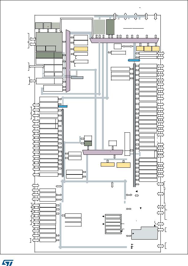
Figure 1 shows the device block diagram.
DS12923 Rev 1 |
15/252 |

|
Description |
|
|
|
|
|
|
|
|
STM32H745xI/G |
|
||
|
|
|
|
|
|
|
|
|
|
|
|
|
|
|
|
Table 2. STM32H745xI/G features and peripheral counts |
|
|
|
|
|||||||
|
Peripherals |
STM32H745ZG |
STM32H745IG |
STM32H745BG |
STM32H745XG |
|
STM32H745ZI |
STM32H745II |
|
STM32H745BI |
STM32H745XI |
|
|
|
|
|
|
|
|
|
|
|
|
|
|
||
|
|
|
|
|
|
|
|
|
|
|
|
||
|
Flash memory in Kbytes |
|
2 x 512 Kbytes |
|
|
|
2 x 1 Mbyte |
|
|
||||
|
|
|
|
|
|
|
|
|
|
|
|
|
|
|
|
SRAM |
|
|
|
|
|
|
|
|
|
|
|
|
|
mapped |
|
|
|
|
512 |
|
|
|
|
|
|
|
|
onto AXI bus |
|
|
|
|
|
|
|
|
|
|
|
|
|
|
|
|
|
|
|
|
|
|
|
|
|
|
|
SRAM1 |
|
|
|
|
128 |
|
|
|
|
|
|
|
|
(D2 domain) |
|
|
|
|
|
|
|
|
|
||
|
SRAM in |
|
|
|
|
|
|
|
|
|
|
|
|
|
|
|
|
|
|
|
|
|
|
|
|
|
|
|
SRAM2 |
|
|
|
|
|
|
|
|
|
|
|
|
|
Kbytes |
|
|
|
|
128 |
|
|
|
|
|
||
|
(D2 domain) |
|
|
|
|
|
|
|
|
|
|||
|
|
|
|
|
|
|
|
|
|
|
|
|
|
|
|
|
|
|
|
|
|
|
|
|
|
|
|
|
|
SRAM3 |
|
|
|
|
32 |
|
|
|
|
|
|
|
|
(D2 domain) |
|
|
|
|
|
|
|
|
|
||
|
|
|
|
|
|
|
|
|
|
|
|
|
|
|
|
|
|
|
|
|
|
|
|
|
|
|
|
|
|
SRAM4 |
|
|
|
|
64 |
|
|
|
|
|
|
|
|
(D3 domain) |
|
|
|
|
|
|
|
|
|
||
|
|
|
|
|
|
|
|
|
|
|
|
|
|
|
|
|
|
|
|
|
|
|
|
|
|
|
|
|
|
ITCM RAM |
|
|
|
|
64 |
|
|
|
|
|
|
|
TCM RAM in |
(instruction) |
|
|
|
|
|
|
|
|
|
||
|
|
|
|
|
|
|
|
|
|
|
|
||
|
Kbytes |
|
|
|
|
|
|
|
|
|
|
|
|
|
DTCM RAM |
|
|
|
|
128 |
|
|
|
|
|
||
|
|
|
|
|
|
|
|
|
|
|
|||
|
|
(data) |
|
|
|
|
|
|
|
|
|
||
|
|
|
|
|
|
|
|
|
|
|
|
|
|
|
|
|
|
|
|
|
|
|
|
|
|
|
|
|
Backup SRAM (Kbytes) |
|
|
|
|
4 |
|
|
|
|
|
||
|
|
|
|
|
|
|
|
|
|
|
|
||
|
FMC |
|
|
|
|
Yes |
|
|
|
|
|
||
|
|
|
|
|
|
|
|
|
|
|
|
|
|
|
General-purpose |
97 |
119/128 |
148 |
168 |
|
97 |
119/128 |
|
148 |
168 |
|
|
|
input/outputs |
|
|
|
|||||||||
|
|
|
|
|
|
|
|
|
|
|
|
||
|
|
|
|
|
|
|
|
|
|
|
|
|
|
|
Quad-SPI |
|
|
|
|
Yes |
|
|
|
|
|
||
|
|
|
|
|
|
|
|
|
|
|
|
||
|
Ethernet |
|
|
|
|
Yes |
|
|
|
|
|
||
|
|
|
|
|
|
|
|
|
|
|
|
|
|
|
|
High- |
|
|
|
|
1 |
|
|
|
|
|
|
|
|
resolution |
|
|
|
|
|
|
|
|
|
||
|
|
|
|
|
|
|
|
|
|
|
|
|
|
|
|
|
|
|
|
|
|
|
|
|
|
|
|
|
|
General- |
|
|
|
|
10 |
|
|
|
|
|
|
|
|
purpose |
|
|
|
|
|
|
|
|
|
||
|
|
|
|
|
|
|
|
|
|
|
|
|
|
|
|
|
|
|
|
|
|
|
|
|
|
|
|
|
Timers |
Advanced- |
|
|
|
|
|
|
|
|
|
|
|
|
|
control |
|
|
|
|
2 |
|
|
|
|
|
|
|
|
(PWM) |
|
|
|
|
|
|
|
|
|
|
|
|
|
|
|
|
|
|
|
|
|
|
|
|
|
|
|
Basic |
|
|
|
|
2 |
|
|
|
|
|
|
|
|
|
|
|
|
|
|
|
|
|
|
|
|
|
|
Low-power |
|
|
|
|
5 |
|
|
|
|
|
|
|
|
|
|
|
|
|
|
|
|
|
|
|
|
|
Wakeup pins |
|
4 |
|
6 |
|
|
4 |
|
|
6 |
|
|
|
Tamper pins |
|
2 |
|
3 |
|
|
2 |
|
|
3 |
|
|
|
|
|
|
|
|
|
|
|
|
|
|
|
|
16/252 |
DS12923 Rev 1 |

|
STM32H745xI/G |
|
|
|
|
|
|
|
|
|
|
|
Description |
|
||
|
|
|
|
|
|
|
|
|
|
|
|
|
|
|||
|
|
Table 2. STM32H745xI/G features and peripheral counts (continued) |
|
|
|
|||||||||||
|
Peripherals |
STM32H745ZG |
|
STM32H745IG |
STM32H745BG |
STM32H745XG |
|
STM32H745ZI |
|
STM32H745II |
STM32H745BI |
STM32H745XI |
|
|||
|
|
|
|
|
|
|
|
|
|
|
|
|
|
|
||
|
|
|
|
|
|
|
|
|
|
|
|
|
|
|
|
|
|
Random number generator |
|
|
|
|
|
|
Yes |
|
|
|
|
|
|
||
|
|
|
|
|
|
|
|
|
|
|
|
|
|
|
|
|
|
|
SPI / I2S |
|
|
|
|
|
|
6/3(1) |
|
|
|
|
|
|
|
|
|
I2C |
|
|
|
|
|
|
4 |
|
|
|
|
|
|
|
|
|
USART/ |
|
|
|
|
|
|
4/4 |
|
|
|
|
|
|
|
|
|
UART/ |
|
|
|
|
|
|
|
|
|
|
|
|
||
|
|
|
|
|
|
|
|
/1 |
|
|
|
|
|
|
||
|
|
LPUART |
|
|
|
|
|
|
|
|
|
|
|
|
||
|
|
|
|
|
|
|
|
|
|
|
|
|
|
|
|
|
|
|
|
|
|
|
|
|
|
|
|
|
|
|
|
|
|
|
|
SAI |
|
|
|
|
|
|
4 |
|
|
|
|
|
|
|
|
|
|
|
|
|
|
|
|
|
|
|
|
|
|
||
|
|
SPDIFRX |
|
|
|
|
|
4 inputs |
|
|
|
|
|
|
||
|
Communicati |
|
|
|
|
|
|
|
|
|
|
|
|
|
|
|
|
SWPMI |
|
|
|
|
|
|
Yes |
|
|
|
|
|
|
||
|
on interfaces |
|
|
|
|
|
|
|
|
|
|
|
|
|
|
|
|
MDIO |
|
|
|
|
|
|
Yes |
|
|
|
|
|
|
||
|
|
|
|
|
|
|
|
|
|
|
|
|
|
|||
|
|
|
|
|
|
|
|
|
|
|
|
|
|
|
|
|
|
|
SDMMC |
|
|
|
|
|
|
2 |
|
|
|
|
|
|
|
|
|
|
|
|
|
|
|
|
|
|
|
|
|
|
|
|
|
|
FDCAN/TT- |
|
|
|
|
|
|
1/1 |
|
|
|
|
|
|
|
|
|
FDCAN |
|
|
|
|
|
|
|
|
|
|
|
|
||
|
|
|
|
|
|
|
|
|
|
|
|
|
|
|
|
|
|
|
|
|
|
|
|
|
|
|
|
|
|
|
|
|
|
|
|
USB |
|
|
|
|
|
|
Yes |
|
|
|
|
|
|
|
|
|
OTG_FS |
|
|
|
|
|
|
|
|
|
|
|
|
||
|
|
|
|
|
|
|
|
|
|
|
|
|
|
|
|
|
|
|
|
|
|
|
|
|
|
|
|
|
|
|
|
|
|
|
|
USB |
|
|
|
|
|
|
Yes |
|
|
|
|
|
|
|
|
|
OTG_HS |
|
|
|
|
|
|
|
|
|
|
|
|
||
|
|
|
|
|
|
|
|
|
|
|
|
|
|
|
|
|
|
|
|
|
|
|
|
|
|
|
|
|
|
|
|
|
|
|
Ethernet and camera |
|
|
|
|
|
|
Yes |
|
|
|
|
|
|
||
|
interface |
|
|
|
|
|
|
|
|
|
|
|
|
|||
|
|
|
|
|
|
|
|
|
|
|
|
|
|
|
||
|
|
|
|
|
|
|
|
|
|
|
|
|
|
|
||
|
LCD-TFT |
|
|
|
|
|
|
Yes |
|
|
|
|
|
|
||
|
|
|
|
|
|
|
|
|
|
|
|
|
|
|
||
|
JPEG Codec |
|
|
|
|
|
|
Yes |
|
|
|
|
|
|
||
|
|
|
|
|
|
|
|
|
|
|
|
|
|
|
|
|
|
Chrom-ART Accelerator™ |
|
|
|
|
|
|
Yes |
|
|
|
|
|
|
||
|
(DMA2D) |
|
|
|
|
|
|
|
|
|
|
|
|
|||
|
|
|
|
|
|
|
|
|
|
|
|
|
|
|
||
|
|
|
|
|
|
|
|
|
|
|
|
|
|
|
||
|
16-bit ADCs |
|
|
|
|
|
|
3 |
|
|
|
|
|
|
||
|
Number of Direct channels |
2 |
2 |
|
4 |
2 |
4 |
|
2 |
2 |
|
4 |
2 |
4 |
|
|
|
Number of Fast channels |
6 |
9 |
|
9 |
9 |
9 |
|
6 |
9 |
|
9 |
9 |
9 |
|
|
|
Number of Slow channels |
15 |
17 |
|
23 |
21 |
23 |
|
15 |
17 |
|
23 |
21 |
23 |
|
|
|
|
|
|
|
|
|
|
|
|
|
|
|
|
|
|
|
|
12-bit DAC |
|
|
|
|
|
|
Yes |
|
|
|
|
|
|
||
|
Number of channels |
|
|
|
|
|
|
2 |
|
|
|
|
|
|
||
|
|
|
|
|
|
|
|
|
|
|
|
|
|
|
||
|
Comparators |
|
|
|
|
|
|
2 |
|
|
|
|
|
|
||
|
|
|
|
|
|
|
|
|
|
|
|
|
|
|
||
|
Operational amplifiers |
|
|
|
|
|
|
2 |
|
|
|
|
|
|
||
|
|
|
|
|
|
|
|
|
|
|
|
|
|
|
||
|
DFSDM |
|
|
|
|
|
|
Yes |
|
|
|
|
|
|
||
|
|
|
|
|
|
|
|
|
|
|
|
|
|
|
|
|
DS12923 Rev 1 |
17/252 |
Description |
STM32H745xI/G |
|
|
Table 2. STM32H745xI/G features and peripheral counts (continued)
Peripherals
Maximum CPU frequency
Operating voltage
Ambient Operating temperature
temperatures Junction temperature
Ambient Extended temperature operating
temperatures Junction temperature
Package
STM32H745ZG |
STM32H745IG |
STM32H745BG |
STM32H745XG |
STM32H745ZI |
STM32H745II |
STM32H745BI |
STM32H745XI |
480 MHz(2)
400 MHz(3)
300MHz(4)
1.62to 3.6 V(5)
–40 up to +85 °C(6)
–40 to + 125 °C
–40 to + 125 °C(4)(7)
–40 to + 140 °C(8)
LQFP |
LQFP |
UFBGA |
LQFP |
TFBGA |
LQFP |
LQFP |
UFBGA |
LQFP |
TFBGA |
144 |
176 |
176+25 |
208 |
240+25 |
144 |
176 |
176+25 |
208 |
240+25 |
|
|
|
|
|
|
|
|
|
|
1.The SPI1, SPI2 and SPI3 interfaces give the flexibility to work in an exclusive way in either the SPI mode or the I2S audio mode.
2.The product junction temperature must be kept within the –40 to +105 °C range.
3.The product junction temperature must be kept within the –40 to +125 °C range.
4.Up to 300 MHz for STM32H745xxx3 sales types (extended industrial temperature range).
5.VDD/VDDA can drop down to 1.62 V by using an external power supervisor (see Section 3.5.2: Power supply supervisor) and connecting PDR_ON pin to VSS. Otherwise the supply voltage must stay above 1.71 V with the embedded power voltage detector enabled.
6.Using appropriate cooling methods to guarantee that the maximum junction temperature (125 °C) is not exceeded, the maximum ambient temperature (85°C) can be exceeded.
7.The product junction temperature must be kept within the –40 to +140 °C range.
8.It is mandatory to use the SMPS step-down converter when the maximum junction temperature is higher than 125 °C.
18/252 |
DS12923 Rev 1 |
STM32H745xI/G |
Description |
|
|
Figure 1. STM32H745xI/G block diagram
JTDO/SWD, JTDO
JTRST, JTDI,
JTCK/SWCLK
TRACECK
TRACED[3:0]
LCD_R[7:0], LCD_G[7:0],
LCD_B[7:0], LCD_HSYNC,
LCD_VSYNC, LCD_DE,
LCD_CLK
SDMMC_D[7:0],SDMMC_D[7:3,1]Dir
SDMMC_D0dir, SDMMC_D2dir
CMD, CMDdir, CK, Ckin,
CKio as AF
HSYNC, VSYNC, PUIXCLK, D[13:0]
HRTIM1_CH[A..E]x
HRTIM1_FLT[5:1],
HRTIM1_FLT[5:1]_in, SYSFLT
DFSDM1_CKOUT,
DFSDM1_DATAIN[0:7],
DFSDM1_CKIN[0:7]
SD, SCK, FS, MCLK as AF
SD, SCK, FS, MCLK as AF
I- |
D- |
D- |
|
|
TCM |
TCM |
TCM |
|
|
64KB |
64KB |
64KB |
|
|
|
|
AHBP |
|
AXI/AHB12 (200MHz) |
|
Arm |
|
|
Up to 1 MB |
JTAG/SW |
|
|
FLASH |
|
Cortex |
AXIM |
|
||
|
M7 |
|
Up to 1 MB |
|
|
|
|
||
ETM |
|
|
|
FLASH |
I-Cache D-Cache |
|
|
512 KB AXI |
|
16KB |
16KB |
AHBS |
MATRIX- |
SRAM |
CHROM-ART |
16 Streams |
FMC |
||
MDMA |
FIFO |
|
|
|
|
|
|
FMC_signals |
|
|
|
|
|
|
(DMA2D) |
FIFO |
BUS |
Quad-SPI |
|
|
|
|
||
|
|
|
AXI |
CLK, CS,D[7:0] |
|
LCD-TFT |
FIFO |
AXI/AHB34 (200MHz) |
|
|
|
|
64-bit |
|
|
WWDG1 |
JPEG |
AHB3 |
|
|
|
|
|
AHB/APB |
SDMMC1 |
FIFO |
|
|
|
|
ART |
|
|
|
|
(instruction cache) |
|
|
|
|
|
|
AHB ART (200MHz) |
|
Delay block |
|
AHB2 (200MHz) |
||
|
|
|||
|
DCMI |
AHB/APB |
|
|
|
|
|
||
|
HRTIM1 |
|
|
|
|
DFSDM1 |
|
|
|
|
SAI3 |
FIFO |
|
|
|
SAI2 |
FIFO |
|
|
SD, SCK, FS, MCLK, D[3:1], |
|
SAI1 |
FIFO |
|
CK[2:1] as AF |
|
|
|
|
MOSI, MISO, SCK, NSS as AF |
|
SPI5 |
|
(max) |
|
|
|
|
|
1 compl. chan.(TIM17_CH1N), |
|
TIM17 |
|
MHz |
1 chan. (TIM17_CH1, BKIN as AF |
|
|
|
|
1 compl. chan.(TIM16_CH1N), |
|
TIM16 |
|
100 |
1 chan. (TIM16_CH1, BKIN as AF |
|
|
||
2 compl. chan.(TIM15_CH1[1:2]N), |
|
TIM15 |
|
APB2 |
2 chan. (TIM_CH15[1:2], BKIN as AF |
|
SPI4 |
|
|
|
|
|
|
|
MOSI, MISO, SCK, NSS as AF |
|
|
|
|
MOSI, MISO, SCK, NSS / |
|
SPI/I2S1 |
|
|
SDO, SDI, CK, WS, MCK, as AF |
|
smcardirDA USART6 |
|
|
RX, TX, SCK, CTS, RTS as AF |
|
|
|
|
RX, TX, SCK, CTS, RTS as AF |
|
irDAsmcardUSART1 |
|
|
4 compl. chan. (TIM1_CH1[1:4]N), |
|
TIM1/PWM 16b |
|
|
|
|
|||
4 chan. (TIM1_CH1[1:4]ETR, BKIN as AF |
|
|
||
4 compl. chan.(TIM8_CH1[1:4]N), |
|
TIM8/PWM 16b |
|
|
4 chan. (TIM8_CH1[1:4], ETR, BKIN as |
|
|
||
AF |
|
|
|
|
|
|
|
|
|
|
AHB4 |
DMA |
|
Mux2 |
|
|
|
|
AHB4 |
|
BDMA |
AHB4 |
|
|
IWDG1 |
|
|
IWDG2 |
|
AHB4 (200MHz) |
|
|
|
HSEM |
|
|
CRC |
|
|
Up to 17 analog inputs |
ADC3 |
|
common to ADC1 and 2 |
|
|
VDDREF_ADC |
Tem. sensor |
AHB4 |
|
||
PA..J[15:0] |
GPIO PORTA.. J |
|
PK[7:0]
SD, SCK, FS, MCLK,
PDM_DI/CK[4:1] as AF
COMPx_INP, COMPx_INM,
COMPx_OUT as AF
LPTIM5_OUT as AF
LPTIM4_OUT as AF
LPTIM3_OUT as AF
SCL, SDA, SMBAL as AF
MISO, MOSI, SCK, NSS as AF
RX, TX, CK, CTS, RTS as AF
LPTIM2_OUT as AF
GPIO PORTK
SAI4
COMP1&2
LPTIM5
LPTIM4
LPTIM3
I2C4
SPI6
LPUART1
LPTIM2
 APB4 1000MHzMHz(max)
VREF
SYSCFG
EXTI WKUP
|
MII / RMII |
|
SDMMC_ |
DP, DM, STP, |
DP, DM, ID, |
|||
To APB1-2 |
|
MDIO |
|
D[7:0], |
NXT,ULPI:CK |
|||
|
|
, D[7:0], DIR, |
VBUS |
|||||
peripherals |
|
as AF |
CMD, CK as AF |
|||||
|
|
|
|
|
|
ID, VBUS |
|
|
AHB1 |
(200MHz) |
|
|
|
|
|
ETHER |
|
|
PHY |
PHY |
|
|
Arm |
|
DMA1 |
DMA2 |
SDMMC2 |
OTG_HS |
OTG_FS |
|||
|
Cortex |
|
|
MAC |
|
|
|
|
||
|
|
|
|
|
|
|
|
|||
|
M4 |
|
8 Stream |
8 Stream |
DMA |
FIFO |
|
DMA/ |
DMA/ |
|
I- |
D- |
S- |
||||||||
FIFOs |
FIFOs |
FIFO |
FIFO |
|||||||
Bus |
Bus |
Bus |
|
|
|
|||||
|
|
|
|
|
|
|
|
|
|
|
32-bit AHB BUS-MATRIX
AHB4 (200MHz) |
AHB2 (200MHz) |
AHB ART(200MHz)
DMA |
|
(200MHz) |
SRAM1 SRAM2 SRAM3 |
|
Mux1 |
|
|
||
|
|
|
128 KB 128 KB 32 KB |
|
RNG |
|
AHB1 |
|
ADC1 |
|
|
|
ADC2 |
|
|
|
|
|
|
|
|
AHB/APB |
|
|
|
|
|
32b |
TIM2 |
TIM6 |
|
|
|
|
16b |
|
16b |
TIM3 |
|
|
|
|||
|
|
|
|
|
TIM7 |
16b |
|
16b |
TIM4 |
|
|
|||
|
|
|
|
|
SWPMI |
|
|
|
TIM5 |
|
|
|
32b |
|
|
|
|
|
|
|
|
|
16b |
TIM12 |
|
|
|
|
|
|
|
|
16b |
TIM13 |
|
|
|
|
|
|
|
|
16b |
TIM14 |
|
|
|
|
|
|
|
|
|
smcard |
|
|
|
|
USART2 |
|
|
|
|
irDA |
|
|
|
|
smcard |
|
|
|
|
USART3 |
|
|
|
|
irDA |
Up to 20 analog inputs common to ADC1 & 2
4 channels, ETR as AF
4 channels, ETR as AF
4 channels, ETR as AF
4 channels
2 channels as AF
1 channel as AF
1 channel as AF
RX, TX, SCK, CTS,
RTS as AF
RX, TX, SCK
CTS, RTS as AF
AHB4 |
AHB4 |
DAP
|
A P B 10 MHz3 |
SRAM |
100 MHz (max) |
10 KB |
APB1 |
UART4
UART5
UART7
UART8
SPI2/I2S2
SPI3/I2S3
I2C1/SMBUS
I2C2/SMBUS
I2C3/SMBUS
MDIOS
 filter Digital
RX, TX as AF
RX, TX as AF
RX, TX as AF
RX, TX as AF
MOSI, MISO, SCK, NSS/SDO,
SDI, CK, WS, MCK, as AF
MOSI, MISO, SCK, NSS/SDO,
SDI, CK, WS, MCK, as AF
SCL, SDA, SMBAL as AF
SCL, SDA, SMBAL as AF
SCL, SDA, SMBAL as AF
MDC, MDIO
32-bit AHB BUS-MATRIX |
RAM |
FDCAN1 |
FIFO |
TX, RX |
|
I/F |
FDCAN2 |
TX, RX |
|
|
|
|||
|
|
|
|
|
CRS |
|
64 KB SRAM |
4 KB BKP |
SPDIFRX1 |
IN[1:4] as AF |
|
RAM |
HDMI-CEC |
CEC as AF |
|
|
||
|
|
DAC1&2 |
DAC1_OUT, DAC2_OUT as AF |
|
|
LPTIM1 16b |
LPTIM1_IN1, LPTIM1_IN2, |
|
|
LPTIM1_OUT as AF |
OPAMP1&2
|
|
(200MHz) |
|
VDD12 |
POWER MANAGEMENT |
||||
|
|
|
|
|
|
|
|
|
WWDG2 |
|
|
|
|
|
|
|
|
@VDD33 |
|
|
|
|
|
|
|
|
|
||
RCC |
|
AHB/APBAHB4 |
|
|
|
|
|
|
|
Reset & |
|
|
PWRCTRL |
|
|
|
Voltage regulator |
||
control |
|
|
|
|
SMPS step-down |
||||
|
|
|
|
|
|
|
|
3.3 to 1.2V |
|
|
|
|
|
|
|
|
|
|
converter |
|
|
|
|
|
|
|
|
|
|
|
|
|
|
|
|
|
|
|
|
|
|
|
@VSW |
|
|
||||
@VDD
CSI |
|
|
4 MHz CSI |
|
RC48
 48 MHz HSI48 RC
HSI |
|
|
64 MHz HSI RC |
|
|||
|
|
|
|
LSI 
 32 KHz LSI RC
PLL1+PLL2+PLL3
|
|
|
|
|
|
|
|
|
|
|
|
|
|
LS |
|
|
XTAL 32 kHz |
|
|||
|
|
|
|
|
RTC |
|
||||
|
|
|
|
|
|
|
|
|||
(max) |
|
|
|
|
Backup registers |
|
||||
|
|
LS |
|
|||||||
|
|
AWU |
|
|||||||
|
|
|
|
|
|
|||||
100 MHz |
|
|
|
|
|
|
|
|
|
|
|
|
|
|
|
@VDD |
|||||
APB4 |
|
|
|
|
|
|
|
|
|
|
|
|
|
|
|
|
XTAL OSC |
|
|||
|
|
|
|
|
|
|
4- 48 MHz |
|
||
|
|
|
|
|
|
|
|
|
|
|
|
|
|
|
|
|
IWDG1 |
|
|
|
|
|
|
|
|
|
|
|
|
|||
|
|
|
|
|
|
IWDG2 |
|
|
|
|
|
|
|
@VDD |
|
|
|
|
|
|
|
|
POR |
SUPPLY SUPERVISION |
|
|||||||
|
reset |
|
|
POR/PDR/BOR |
|
|
||||
|
Int |
|
|
|
PVD |
|
|
|
||
|
|
|
|
|
|
|
|
|||
|
|
|
|
|
|
|
|
|
|
|
OPAMPx_VINM
OPAMPx_VINP
OPAMPx_VOUT as AF
VDD = 1.62 to 3.6V VDD33USB = 3.0 to 3.6V VSS
VCAP
VDDMMC33 = 1.8 to 3.6V VDDSMPS, VSSSMPS VLXSMP, VFBSMPS,
OSC32_IN
OSC32_OUT
RTC_TS
RTC_TAMP[1:3]
RTC_OUT
RTC_REFIN
VBAT = 1.2 to 3.6 V
OSC_IN
OSC_OUT
VDDA, VSSA
NRESET
WKUP[5:0]
MSv43754V13
DS12923 Rev 1 |
19/252 |

Description |
STM32H745xI/G |
|
|
Compatibility throughout the family
STM32H745xI/G devices are not pin-to-pin compatible with STM32H7x3 devices (single core line):
•The TFBGA240+25 ballout is compatible with STM32H7x3 devices, except for a few I/O balls as shown in Figure 2.
•LQFP208 and LQFP176 pinouts, as well as UFBGA176+25 ballout are not compatible with STM32H7x3 devices.
Figure 2. TFBGA240+25 ball assignment differences
|
|
1 |
2 |
3 |
4 |
5 |
6 |
7 |
8 |
9 |
10 |
11 |
12 |
13 |
14 |
15 |
16 |
17 |
|
|
|
|
|||||||||||||||||
A |
VSS |
PI6 |
PI5 |
PI4 |
PB5 |
VDDLDO |
VCAP |
PK5 |
PG10 |
PG9 |
PD5 |
PD4 |
PC10 |
PA15 |
PI1 |
PI0 |
VSS |
|
|
|
|
|
|
|
|
|
|
|
|
|
|
|
|
|
|
|
|
|
|
B |
VBAT |
VSS |
PI7 |
PE1 |
PB6 |
VSS |
PB4 |
PK4 |
PG11 |
PJ15 |
PD6 |
PD3 |
PC11 |
PA14 |
PI2 |
PH15 |
PH14 |
|
|
|
|
|
|
|
|
|
|
|
|
|
|
|
|
|
|
|
|
|
|
|
|
PC15- |
PC14- |
|
|
|
|
|
|
|
|
|
|
|
|
|
|
|
|
C |
OSC32_ |
OSC32_ |
PE2 |
PE0 |
PB7 |
PB3 |
PK6 |
PK3 |
PG12 |
VSS |
PD7 |
PC12 |
VSS |
PI3 |
PA13 |
VSS |
VDDLDO |
|
|
|
|
OUT |
IN |
|
|
|
|
|
|
|
|
|
|
|
|
|
|
|
|
D |
PE5 |
PE4 |
PE3 |
PB9 |
PB8 |
PG15 |
PK7 |
PG14 |
PG13 |
PJ14 |
PJ12 |
PD2 |
PD0 |
PA10 |
PA9 |
PH13 |
VCAP |
|
|
|
|
|
|
|
|
|
|
|
|
|
|
|
|
|
|
|
|
|
|
E |
|
PI9 |
PC13 |
PI8 |
PE6 |
VDD |
PDR |
BOOT0 |
VDD |
PJ13 |
VDD |
PD1 |
PC8 |
PC9 |
PA8 |
PA12 |
PA11 |
|
|
|
_ON |
|
|||||||||||||||||
|
|
|
|
|
|
|
|
|
|
|
|
|
|
|
|
|
|
|
|
F |
|
|
PI10 |
PI11 |
VDD |
|
|
|
|
|
|
|
PC7 |
PC6 |
PG8 |
PG7 |
VDD33 |
|
|
|
|
|
|
|
|
|
|
|
USB |
|
|||||||||
|
|
|
|
|
|
|
|
|
|
|
|
|
|
|
|
|
|
|
|
G |
PF2 |
|
PF1 |
PF0 |
VDD |
|
VSS |
VSS |
VSS |
VSS |
VSS |
|
VDD |
PG5 |
PG6 |
VSS |
VDD50 |
|
|
|
|
|
USB |
|
|||||||||||||||
H |
PI12 |
PI13 |
PI14 |
PF3 |
VDD |
|
VSS |
VSS |
VSS |
VSS |
VSS |
|
VDD |
PG4 |
PG3 |
PG2 |
PK2 |
|
|
|
|
|
|
|
|
|
|
|
|
|
|
|
|
|
|
|
|
|
|
|
|
PH1- |
PH0- |
|
|
|
|
|
|
|
|
|
|
|
|
|
|
|
|
J |
OSC_ |
VSS |
PF5 |
PF4 |
|
VSS |
VSS |
VSS |
VSS |
VSS |
|
VDD |
PK0 |
PK1 |
VSS |
VSS |
|
||
OSC_IN |
|
|
|
||||||||||||||||
|
|
OUT |
|
|
|
|
|
|
|
|
|
|
|
|
|
|
|
|
|
K |
NRST |
PF6 |
PF7 |
PF8 |
VDD |
|
VSS |
VSS |
VSS |
VSS |
VSS |
|
VDD |
PJ11 |
VSS |
NC |
NC |
|
|
|
|
|
|
|
|
|
|
|
|
|
|
|
|
|
|
|
|
|
|
L |
VDDA |
PC0 |
PF10 |
PF9 |
VDD |
|
VSS |
VSS |
VSS |
VSS |
VSS |
|
VDD |
PJ10 |
VSS |
NC |
NC |
|
|
|
|
|
|
|
|
|
|
|
|
|
|
|
|
|
|
|
|
|
|
M |
VREF+ |
PC1 |
PC2 |
PC3 |
VDD |
|
|
|
|
|
|
|
VDD |
PJ9 |
VSS |
NC |
NC |
|
|
|
|
|
|
|
|
|
|
|
|
|
|
|
|
|
|
|
|
|
|
N |
VREF- |
PH2 |
PA2 |
PA1 |
PA0 |
PJ0 |
VDD |
VDD |
PE10 |
VDD |
VDD |
VDD |
PJ8 |
PJ7 |
PJ6 |
VSS |
NC |
|
|
|
|
|
|
|
|
|
|
|
|
|
|
|
|
|
|
|
|
|
|
P |
VSSA |
PH3 |
PH4 |
PH5 |
PI15 |
PJ1 |
PF13 |
PF14 |
PE9 |
PE11 |
PB10 |
PB11 |
PH10 |
PH11 |
PD15 |
PD14 |
VDD |
|
|
|
|
|
|
|
|
|
|
|
|
|
|
|
|
|
|
|
|
|
|
R |
PC2_C |
PC3_C |
PA6 |
VSS |
PA7 |
PB2 |
PF12 |
VSS |
PF15 |
PE12 |
PE15 |
PJ5 |
PH9 |
PH12 |
PD11 |
PD12 |
PD13 |
|
|
|
|
|
|
|
|
|
|
|
|
|
|
|
|
|
|
|
|
|
|
T |
PA0_C |
PA1_C |
PA5 |
PC4 |
PB1 |
PJ2 |
PF11 |
PG0 |
PE8 |
PE13 |
PH6 |
VSS |
PH8 |
PB12 |
PB15 |
PD10 |
PD9 |
|
|
|
|
|
|
|
|
|
|
|
|
|
|
|
|
|
|
|
|
|
|
U |
VSS |
PA3 |
PA4 |
PC5 |
PB0 |
PJ3 |
PJ4 |
PG1 |
PE7 |
PE14 |
VCAP |
VDDLDO |
PH7 |
PB13 |
PB14 |
PD8 |
VSS |
|
|
|
|
|
|
|
|
|
|
|
|
|
|
|
|
|
|
|
|
|
|
STM32H7x5 |
STM32H7x3 |
|||
|
|
|
|
|
VLX |
PI9 |
|
NC |
PI9 |
SMPS |
|
|||
|
|
|
|
|
VDD |
VSS |
|
NC |
NC |
SMPS |
SMPS |
|
||
|
|
|
||
PF2 |
VFB |
|
PF2 |
NC |
SMPS |
|
|||
|
|
|
|
|
MSv48801V2
1. The balls highlighted in gray correspond to different signals on STM32H745xI/G and STM32H7x3 devices.
20/252 |
DS12923 Rev 1 |