


Digital I/O/PFI
Static Characteristics
Number of channels |
48 total, 32 (P0.<0..31>), |
|
16 (PFI <0..7>/P1, PFI <8..15>/P2) |
|
|
Ground reference |
D GND |
|
|
Direction control |
Each terminal individually programmable as |
|
input or output |
|
|
Pull-down resistor |
50 kΩ typical, 20 kΩ minimum |
|
|
Input voltage protection |
±20 V on up to two pins2 |
Waveform Characteristics (Port 0 Only)
Terminals used |
Port 0 (P0.<0..31>) |
Port/sample size |
Up to 32 bits |
|
|
Waveform generation (DO) FIFO |
2,047 samples |
|
|
Waveform acquisition (DI) FIFO |
2,047 samples |
|
|
DI Sample Clock frequency |
|
|
|
PCI/PCI Express/PXI/PXI Express |
0 MHz to 10 MHz, system and bus activity |
|
dependent |
|
|
USB |
0 MHz to 1 MHz, system and bus activity |
|
dependent |
|
|
DO Sample Clock frequency |
|
|
|
PCI/PCI Express/PXI/PXI Express |
|
|
|
Regenerate from FIFO |
0 MHz to 10 MHz |
|
|
Streaming from memory |
0 to 10 MHz, system and bus activity |
|
dependent |
|
|
USB |
|
|
|
Regenerate from FIFO |
0 MHz to 10 MHz |
|
|
Streaming from memory |
0 MHz to 1 MHz, system and bus activity |
|
dependent |
|
|
2Stresses beyond those listed under Input voltage protection may cause permanent damage to the device.
NI 6259 Device Specifications | © National Instruments | 9

Data transfers
PCI/PCI Express/PXI/PXI Express |
DMA (scatter-gather), interrupts, |
|
programmed I/O |
|
|
USB |
USB Signal Stream, programmed I/O |
|
|
DI or DO Sample Clock source3 |
Any PFI, RTSI, AI Sample or Convert Clock, |
|
AO Sample Clock, Ctr n Internal Output, and |
|
many other signals |
|
|
PFI/Port 1/Port 2 Functionality
Functionality |
Static digital input, static digital output, |
||
|
timing input, timing output |
|
|
|
|
|
|
Timing output sources |
Many AI, AO, counter, DI, DO timing signals |
||
|
|
|
|
Debounce filter settings |
125 ns, 6.425 µs, 2.56 ms, disable; high and |
||
|
low transitions; selectable per input |
||
|
|
|
|
Recommended Operating Conditions |
|
||
|
|
|
|
Level |
|
Minimum |
Maximum |
|
|
|
|
|
|
|
|
Input high voltage (VIH) |
|
2.2 V |
5.25 V |
Input low voltage (VIL) |
|
0 V |
0.8 V |
Output high current (IOH) P0.<0..31> |
|
— |
-24 mA |
Output high current (IOH) PFI <0..15>/P1/P2 |
|
— |
-16 mA |
Output low current (IOL) P0.<0..31> |
|
— |
24 mA |
Output low current (IOL) PFI <0..15>/P1/P2 |
|
— |
16 mA |
Note On earlier versions of the USB-6259 Screw Terminal (part numbers 194021B/C/-0x), the digital I/O characteristics of P0.<16..31> match the characteristics of PFI <0..15>. Refer to the November 2006 version of the NI 625x Specifications (part number 371291G-01) for more details.
3The digital subsystem does not have its own dedicated internal timing engine. Therefore, a sample clock must be provided from another subsystem on the device or an external source.
10 | ni.com | NI 6259 Device Specifications
Electrical Characteristics
Level |
Minimum |
Maximum |
|
|
|
|
|
|
Positive-going threshold (VT+) |
— |
2.2 V |
|
|
|
Negative-going threshold (VT-) |
0.8 V |
— |
|
|
|
Delta VT hystersis (VT+ - VT-) |
0.2 V |
— |
|
|
|
IIL input low current (Vin = 0 V) |
— |
-10 µA |
IIH input high current (Vin = 5 V) |
— |
250 µA |
Digital I/O Characteristics
Figure 5. P0.<0..31>: Ioh versus Voh
Ioh (mA)
0 |
|
|
|
|
|
|
|
|
|
|
|
|
|
|
|
–5 |
|
|
|
|
55 °C; Vdd = 4.5 V |
|
|
|
|
|
|
|
|||
–10 |
|
|
|
|
25 °C; Vdd = 5.0 V |
|
|
|
|
|
|
0 °C; Vdd = 5.5 V |
|
||
–15 |
|
|
|
|
|
||
|
|
|
|
|
|
|
|
|
|
|
|
|
|
|
|
|
|
|
|
|
|
|
|
–20 |
|
|
|
|
|
|
|
|
|
|
|
|
|
|
|
–25 |
|
|
|
|
|
|
|
|
|
|
|
|
|
|
|
–30 |
|
|
|
|
|
|
|
|
|
|
|
|
|
|
|
–35 |
|
|
|
|
|
|
|
|
|
|
|
|
|
|
|
–40 |
|
|
|
|
|
|
|
|
|
|
|
|
|
|
|
–45 |
|
|
|
|
|
|
|
|
|
|
|
|
|
|
|
–50
2 |
3 |
4 |
5 |
6 |
Voh (V)
NI 6259 Device Specifications | © National Instruments | 11
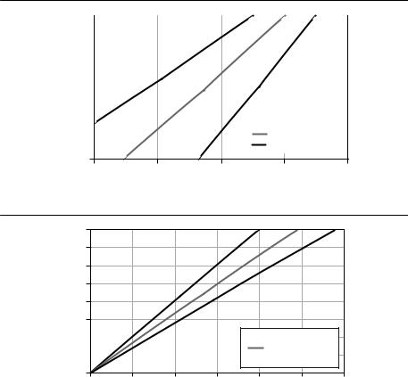
Figure 6. PFI <0..15>/P1/P2: Ioh versus Voh
Ioh (mA)
0 |
|
|
|
|
|
|
|
|
|
|
|
|
|
|
|
|
|
–5 |
|
|
|
|
|
|
|
|
|
|
|
|
|
|
|
||
–10 |
|
|
|
|
|
|
|
|
|
|
|
|
|
|
|
||
–15 |
|
|
|
|
|
|
|
|
|
|
|
|
|
|
|
||
–20 |
|
|
|
|
|
|
|
|
|
|
|
|
|
|
|
||
–25 |
|
|
|
|
|
|
|
|
|
|
|
|
|
|
|
||
–30 |
|
|
|
|
|
|
|
|
|
|
|
|
|
|
|
||
–35 |
|
|
|
|
|
|
|
|
–40 |
|
|
|
|
|
55 °C; Vdd = 4.5 V |
|
|
|
|
|
|
|
25 °C; Vdd = 5.0 V |
|
||
|
|
|
|
|
||||
|
|
|
|
|
|
|
||
–45 |
|
|
|
|
|
0 °C; Vdd = 5.5 V |
|
|
|
|
|
||||||
|
|
|
|
|
|
|
|
|
–50 |
|
|
|
|
2 |
3 |
4 |
5 |
6 |
Voh (V)
Figure 7. P0.<0..31>: Iol versus Vol
Iol (mA)
40
35
30
25
20
15
10 
 55 °C; Vdd = 4.5 V 25 °C; Vdd = 5.0 V
5 
 0 °C; Vdd = 5.5 V
0
0 |
0.2 |
0.4 |
0.6 |
0.8 |
1.0 |
1.2 |
|
|
|
Vol (V) |
|
|
|
12 | ni.com | NI 6259 Device Specifications