

Chapter 4 Hardware Overview
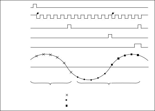
Figure 4-9 shows the relevant timing signals for a typical pretriggered acquisition. The illustration represents five pretrigger and five posttrigger scans, and above-high-level analog triggering is used. See the Analog Trigger Circuit section later in this chapter for more information on analog trigger types.
Start Trigger |
|
First Scan |
First Posttrigger Scan |
Scan Clock |
|
Scan Counter |
|
Terminal Count |
|
Stop Trigger |
|
End of |
|
Acquisition |
|
Trigger Level |
|
Points Discarded |
Five Pretrigger, Five Posttrigger |
|
Points Stored |
|
= Discarded Points |
|
= Pretrigger Points |
|
= Posttrigger Points |
Figure 4-9. Pretrigger Acquisition
NI 5102 User Manual |
4-12 |
ni.com |
Chapter 4 Hardware Overview
|
Table 4-7 describes the pretrigger acquisition signals. |
|
Table 4-7. Pretrigger Acquisition Signals |
|
|
Signal |
Description |
|
|
|
|
Start Trigger |
Starts data acquisition. In pretrigger mode, the Start Trigger signal |
|
enables the storage of pretrigger data. Start Trigger can only be |
|
generated through software in pretrigger mode. |
|
|
Scan Clock |
Causes the ADC to convert the input signal into digital data. This signal |
|
is also used in the memory controller to write the data into onboard |
|
memory. This signal can be generated internally, with a 24-bit down |
|
counter clocked with a 20 MHz signal to generate pulses from 20 MHz |
|
to 1.19 Hz. The 24-bit counter provides a wide choice of valid |
|
frequencies for the Scan Clock signal. In addition, Scan Clock can also |
|
be selected from CH0, CH1, TRIG, PFI1, and PFI2, or any of the seven |
|
RTSI bus trigger lines. RTSI bus trigger lines are available only on the |
|
NI 5102 (PCI, PXI, ISA). |
|
|
Scan Counter |
Is an internally generated signal that pulses once to indicate that the |
Terminal Count |
pretrigger sample count requirement is met. Between the time when |
|
this signal pulses and the Stop Trigger occurs, hardware overwrites the |
|
oldest points in memory with the most recent points in a circular |
|
fashion. All Stop Triggers occurring before Scan Counter Terminal |
|
Count are ignored by the device. |
|
|
Stop Trigger |
Terminates the acquisition sequence after acquiring the posttrigger |
|
sample count. This trigger can be generated through software, or CH0, |
|
CH1, TRIG, PFI1, and PFI2, or any of the seven RTSI bus trigger lines. |
|
RTSI bus trigger lines are available only on the NI 5102 (PCI, |
|
PXI, ISA). |
|
|
End of Acquisition |
Indicates end of acquisition to the control logic in the hardware. |
|
It is generated from a counter that keeps track of points remaining |
|
to acquire. It can be exported from the device on the PFI lines. |
|
|
© National Instruments Corporation |
4-13 |
NI 5102 User Manual |