

диафрагмированные волноводные фильтры / 2e48b8cf-64b7-4662-a02e-ea2085a2e980
.pdfIEEE TRANSACTIONS ON MICROWAVE THEORY AND TECHNIQUES, VOL. 67, NO. 9, SEPTEMBER 2019 |
3783 |
Compact Integrated Full-Duplex Gap
Waveguide-Based Radio Front End For Multi-Gbit/s
Point-to-Point Backhaul Links at E-Band
Abbas Vosoogh , Milad Sharifi Sorkherizi
 , Vessen Vassilev, Ashraf Uz Zaman
 , Member, IEEE, Zhongxia Simon He
 , Member, IEEE, Jian Yang
 , Senior Member, IEEE,
Ahmed A. Kishk , Fellow, IEEE, and Herbert Zirath
 , Fellow, IEEE
Abstract— This paper presents the design and realization of a high data rate radio front-end module for point-to-point backhaul links at E-band. The design module consists of four vertically stacked unconnected metal layers without any galvanic and electrical contact requirements among the building blocks, by using gap waveguide technology. The module components are a high-gain array antenna, diplexer, and circuitry consisting of a transmitter (Tx) and a receiver (Rx) monolithic microwave integrated circuits (MMICs) on a carrier board, which is successfully integrated into one package with a novel architecture and a compact form. The diplexer consists of two direct-coupled cavity bandpass filters with channels at 71–76 GHz and 81–86 GHz with a measured return loss of 15 dB and an isolation greater than 50 dB. A wideband 16 × 16 slot array antenna with a measured gain of more than 31 dBi is used to provide high directivity. The measured results show that the packaged transmitter provides a conversion gain of 22 and 20 dB at 76 and 86 GHz, respectively, with an output power of 14 and 16 dBm at 1-dB gain compression point, at the same frequencies. The packaged receiver shows an average conversion gain of 20 dB at 71–76-GHz and 24 dB at 81–86-GHz bands. A real-time wireless data transmission is successfully demonstrated with a data rate of 8 Gbit/s using 32-quadrature amplitude modulated signal over 1.8-GHz channel bandwidth with spectral efficiency of 4.44 bit/s/Hz. The proposed radio front end provides the advantages of low loss, high efficiency, compact integration, and a simple mechanical assembly, which makes it a suitable solution for small-cell backhaul links.
Index Terms— Frequency-division duplex (FDD), gap waveguide, integration, millimeter-wave, slot array antenna, wireless communication.
Manuscript received September 25, 2018; revised December 16, 2018 and February 25, 2019; accepted April 13, 2019. Date of publication June 13, 2019; date of current version September 4, 2019. (Corresponding author: Abbas Vosoogh.)
A. Vosoogh is with the Department of Microtechnology and Nanoscience, Chalmers University of Technology, 412 96 Gothenburg, Sweden, and also with Metasum AB, 417 60 Gothenburg, Sweden (e-mail: abbas.vosoogh@
chalmers.se). |
|
|
|
M. Sharifi Sorkherizi is with |
Apollo |
Microwaves |
Ltd., Dorval, |
H9P 1H7 QC, Canada. |
|
|
|
V. Vassilev, Z. S. He, and H. |
Zirath are with the Department of |
||
Microtechnology and Nanoscience, |
Chalmers |
University |
of Technology, |
412 96 Gothenburg, Sweden. |
|
|
|
A.U. Zaman, and J. Yang are with the Electrical Engineering Department, Chalmers University of Technology, 412 96 Gothenburg, Sweden.
A.A. Kishk is with the Electrical and Computer Engineering Department, Concordia University, Montreal, QC H3G 1M8, Canada.
Color versions of one or more of the figures in this article are available online at http://ieeexplore.ieee.org.
Digital Object Identifier 10.1109/TMTT.2019.2919539
I. INTRODUCTION
THE increasing demand for higher data traffic and speed in mobile cellular networks leads to a need for higher bandwidth and data rate in the backhaul side of the network. Nowadays, smartphones are not only used for voice calls but also employed for applications that involve extensive data consumption. For example, for a typical fourthgeneration (4G) cellular network, the required backhaul data exceed 250 Mb/s [1]. There is a demand for ultrahigh data rate backhaul point-to-point wireless links as a flexible and cost-effective alternative to fiber-optic networks to provide multi-Gbit/s speed for the fifth-generation (5G) wireless cellular networks. The millimeter-wave frequency band (30–300 GHz) has recently got a lot of attention to provide high-capacity backhaul wireless links with high speed and low
latency.
Millimeter-wave wireless communication systems suffer from high path loss and atmospheric absorption, and they are vulnerable to weather conditions and precipitation [1]. All these factors limit the hop length to a couple of kilometers at millimeter-wave frequencies. However, an atmospheric window exists at E-band (71–76 and 81–86 GHz) with low atmospheric attenuation of around 0.4 dB/km [1]. This makes the E-band a potential candidate to provide multi-Gbit/s data transfer and complements the conventional wireless links that operate in the microwave frequency band. In [2], path loss measurements during ten months versus weather conditions for a 1-km link at 71–76 GHz is presented. The measured attenuation for the rain rate of 20 and 40 mm/h in 1 km is estimated to be 10 and 16.4 dB at 86 GHz, respectively, which are in good agreement with the ITU-R attenuation model in [3].
A lot of effort has been devoted to developing a complete transmitter (Tx) and receiver (Rx) chipsets with different technologies at E-band during the past few years. In [4], an E-band Tx in SiGe BiCMOS technology is presented with an average conversion gain of 23 dB over 71–86-GHz frequency band and maximum 1-dB compression output power of 15 dBm at 72 GHz. Wireless data transmission of 10.12 Gbit/s with 64-QAM modulation over 2-GHz channel is demonstrated using the bench-test measurement setup.
0018-9480 © 2019 IEEE. Personal use is permitted, but republication/redistribution requires IEEE permission. See http://www.ieee.org/publications_standards/publications/rights/index.html for more information.

3784 |
IEEE TRANSACTIONS ON MICROWAVE THEORY AND TECHNIQUES, VOL. 67, NO. 9, SEPTEMBER 2019 |
In [5], 6-Gbit/s data transmission by aggregating four channels with 625-MHz bandwidth has been demonstrated by using 8PSK modulation with bench-test measurement setup. A 2.4-bit/s/Hz spectral efficiency has been achieved in the 81–86-GHz frequency band. A 10-Gbit/s data transmission of 16-QAM modulated signal at 70-/80-GHz bands is shown in [6] with spectral efficiency of 2 bit/s/Hz. Packaged eWLB SiGe transceiver chipsets are presented in [7] for wireless backhaul application in V- and E-bands. Maximum data transmission of 20 Gbit/s with spectral efficiency smaller than 5 bit/s/Hz using 32-QAM modulation is reported in that work.
This paper presents, for the first time, an E-band full-duplex radio front-end module for multi-Gbit/s point-to-point wireless link applications based on the gap waveguide technology. We present a compact integration of passive and active components, as well as a system packaging solution based on gap waveguide technology with a flexible mechanical assembly. An E-band radio transceiver module consisting of a high-gain array antenna, a diplexer, and Tx/Rx chipsets (all in one package) is designed with the capability of sending and receiving data simultaneously at the 71–76- and the 81–86-GHz bands with a frequency-division duplex (FDD) transmission scheme. The design procedure and performance verification of each building block, i.e., diplexer, 16 × 16 slot array antenna, circuitry, and packaging, are presented. In this paper, we have shown the impressive packaging and integration features that gap waveguide technology offers to build up a complex system with simple mechanical assembly.
Section II presents the overall configuration and characteristics of the proposed E-band integrated radio front-end module by using the gap waveguide technology. The design and performance evaluation of a special hybrid diplexer-splitter is presented in Section III. In Section IV, the design and experimental evaluation of a 16 × 16 array antenna and its integration with the diplexer are described. Section V deals with the carrier board design and the Tx and Rx monolithic microwave integrated circuits (MMICs) packaging and performance evaluation. The implementation of a point-to-point real-time wireless link with the proposed compact integrated radio modules is demonstrated in Section VI. Finally, some concluding remarks are given in Section VII.
II. INTEGRATED RADIO FRONT-END MODULE
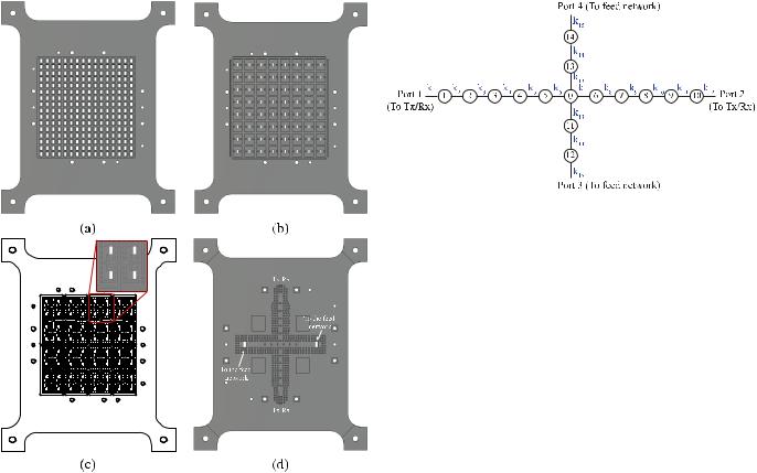
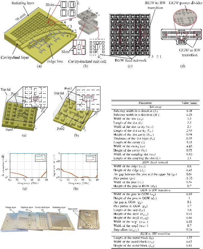
The configuration of the proposed E-band integrated radio front end is shown in Fig. 1. The module consists of a tightly integrated high-gain array antenna, a fifth-order diplexer, and the Tx and Rx chipsets on a carrier board in four distinct layers, where each layer has different functionality. The layers are vertically stacked up and integrated into a compact form. The proposed module has total dimensions of 110 mm × 90 mm × 8.5 mm.
The bottom layer acts as a carrier printed circuit board (PCB) for two complete highly integrated GaAs transmitter and receiver MMICs. We have used commercially available Tx MMIC from Gotmic AB (part no. gTSC0023) with on-wafer 25-dB gain and 16-dBm, 1-dB gain compression
Fig. 1. Configuration of the proposed compact radio front end.
output power. The Tx has a direct conversion architecture with a ×6 frequency multiplier. It covers 71–86-GHz frequency band with IF frequency bandwidth of dc-12 GHz in the input LO frequency band of 11.8–14.3 GHz. Two receiver MMICs are used to cover the frequency band of 71–76 GHz (part no. gRSC0012) and 81–86 GHz (part no. gRSC0013) from the same manufacturer. The Rx MMICs are highly integrated chipsets with a ×6 frequency multiplier, an in-phase and quadrature (IQ) mixer, and IF and low-noise amplifiers with approximately 25-dB conversion gain and 6-dB noise figure. The Tx and Rx MMICs are placed on the carrier board that consists of 100-μm liquid crystal polymer (LCP) substrate on a 1-mm copper plate. More details of the design and layout of the carrier board are presented in Section V.
A fifth-order hybrid diplexer-splitter is designed on the bottom side of layer 2 in groove gap waveguide (GGW). The Tx and Rx MMICs are wire-bonded to microstrip lines, and the RF signals are coupled to the diplexer via a microstrip to the GGW transition. We have tried to minimize the length, where the RF signal propagates within the microstrip lines to reduce the high dielectric and conductive losses of microstrip transmission lines. The designed diplexer has two channels (at 71–76 and 81–86 GHz) with 5-GHz bandwidth. In order to achieve a compact design, the output of the diplexer is directly connected to a power divider so that the diplexer acts as the first stage of the power division for corporate feeding of the array of slots on the top layer. Fig. 2(d) shows the hybrid diplexer-splitter on the backside of layer 2.
A distribution feed network is designed on the backside of layer 3. The outputs of the diplexer are coupled to the next layer, i.e., the feed network, via a right-angle GGW to the rectangular waveguide (RW) transition. The feed network is designed in ridge gap waveguide (RGW) in order to accommodate the corporate feeding of the array antenna elements within a limited available space. We have used a 2 × 2 cavitybacked slot subarray as the radiating element of the designed array antenna. The radiating part consists of 8 × 8 subarrays
VOSOOGH et al.: COMPACT INTEGRATED FULL-DUPLEX GAP WAVEGUIDE-BASED RADIO FRONT END |
3785 |
Fig. 2. Detail illustration of each layer. (a) Radiating slots. (b) Cavities to feed the slots on topside of layer 3. (c) View of the bottom side of layer 3 containing the corporate feednetwork. (d) Diplexer on the bottom side of layer 2.
(16 × 16 slots in total), where they are fed by the same phase and amplitude. The subarrays are formed in two distinct layers, i.e., the cavities (placed at the top side of layer 3) and the radiating layer (on layer 4). The topside of layer 3 contains 8 × 8 cavities that feed the 16 × 16 slots of layer 4 uniformly. The geometry of the feed network and the radiating elements are shown, in more detail, in Fig. 2(a)–(c).
In the proposed module shown in Fig. 1, the different layers do not need to have any electrical and galvanic contact, and a small gap between each layer would not affect the electrical performance of the module. All field leakages and unwanted modes have been suppressed by using a stopband produced by an electromagnetic bandgap (EBG) structure realized in gap waveguide technology, which was introduced, for the first time, in [8] and [9]. Therefore, despite the H -plane split-block configuration of the proposed waveguide module, electrical and galvanic contacts among the layers are not required, which is the major advantage compared to the conventional hollow waveguide technology.
In gap waveguide technology, a guiding structure, such as groove [10], ridge [9], or inverted microstrip line [11], is created between two parallel plates by using an EBG structure, i.e., a periodic pin texture, to control the direction of propagation and preventing any field leakage without the need of electrical contact between the building blocks. This provides a flexible and cost-effective fabrication, and
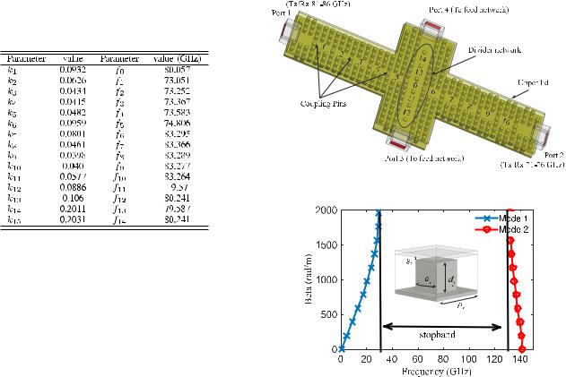
Fig. 3. Coupling diagram of a hybrid diplexer-splitter with a fifth-order divider network and fifth-order channel filters.
mechanical assembly. The advantages of this technology to design high-gain millimeter-wave array antennas [12]–[16], bandpass filters [17]–[24], array antenna, and passive components integration [25]–[27] have been shown in the past few years.
In this paper, we try to show the advantages of gap waveguide technology from the complete system design, integration, and packaging point of views. Due to the complexity of the proposed integrated radio front-end module, we have initially designed and verified the performance of each building block separately. The following sections present the detailed design and measured performance for each critical component within the system.
III. HYBRID DIPLEXER-SPLITTER DESIGN
In this section, the design and optimization of the hybrid diplexer-splitter that is used in the module are explained. We try to keep this section brief and refer the reader to the references for a more detailed technical discussion. The proposed design is based on the prototype developed in [25] and [28]. However, due to the required wideband performance of the diplexer for this paper, we had to expand the design to a more complicated geometry, and as a result, some minor modifications were required to the original methodology. The diplexer channels are required to be allocated at 71–76 and 81–86 GHz with 20-dB return loss and provide at least 50-dB isolation. This translates to 19.2% of overall fractional bandwidth for the diplexer. Such a wide bandwidth requires strong couplings especially in the divider section of the device. After calculating the required polynomial degrees of the filters to achieve the isolation, we tried to use a similar geometry, like the one shown in [28], with a single resonator node as a divider to implement the required electrical specifications. By doing this, we understood that this geometry is unable to provide the required bandwidth for the common couplings. To overcome this issue, we expanded the divider network to be constituted of five resonators, as shown in Fig. 3, to decrease the couplings for each element. Ports 1 and 2 are the outputs of the channel filters, while ports 3 and 4 are the inputs of the divider section.
The next step is to calculate the lumped element network of the hybrid diplexer-splitter. In [28], we proposed a goal function that extracts the coupling matrix (CM) of the
3786 |
IEEE TRANSACTIONS ON MICROWAVE THEORY AND TECHNIQUES, VOL. 67, NO. 9, SEPTEMBER 2019 |
TABLE I
OPTIMIZED PARAMETERS OF THE CM OF THE HYBRID
DIPLEXER-SPLITTER WITH A DIVIDER
NETWORK (SEE FIG. 3)
diplexer-splitter by applying an optimization routine while eliminating the spurious pole between ports 3 and 4. Since we need a divider with an equal 3-dB power division, the divider section is symmetric with respect to the center. It is possible to design the hybrid diplexer-splitter with any desired power division value by removing this symmetry and modifying the goal function to represent the division characteristic. The instruction to choose the correct initial values in order to achieve a fast convergence of the routine is already available in [25] and [28]. The calculated CM is shown in Table I. To avoid the ambiguity regarding the coupling bandwidth, the denormalized k coupling is presented along with the resonant frequencies.
To convert the parameters in Table I to the normal CM parameters, one can use the following equation:
Mi j = Ki j /FBW |
(1) |
in which FBW is the fractional bandwidth. It is important to remark that the diplexer has three different FBW. For the common section (k13–k15), the FBW is computed by including the overall bandwidth of the diplexer ( f1 = 71 GHz and f2 = 86 GHz). We call this as FBW1 = 0.192. For k1–k6, FBW is computed by considering f1 = 71 GHz and f2 = 76 GHz. This will give us FBW2 = 0.068. Finally, for k7–k12, the operating bandwidth is from f1 = 81 GHz to f2 = 86 GHz. Therefore, this provides FBW3 = 0.06. We can translate the input couplings to input resistances using the following equations:
R = M2 |
1 |
|
(2) |
||
Qe = |
|
|
. |
(3) |
|
|
|
|
|||
R |
· |
FBW |
|||
|
|
|
|
|
|
The external Q-factor can be calculated by using the classic formula expressed in (3). Equations (1)–(3) are taken from [29], where further clarifications about these formulas can be found. Furthermore, the following equation has been used to convert the diagonal entries of the CM to physical resonant frequencies:
|
f0 |
|
|
|
|
|
|
|
fk = |
[Mkk · FBW + |
(Mkk · FBW) |
2 |
+ 4] |
(4) |
|||
2 |
|
|
||||||
Fig. 4. Geometry of the proposed hybrid diplexer-splitter.
Fig. 5. Dispersion diagram of the infinite periodic pin unit cell (d f |
= 0.7 mm, |
ar = 0.64 mm, gr = 0.04 mm, and pr = 1.32 mm). |
|
which f0 is the center frequency calculated by
f0 = |
f1 f2 |
. |
(5) |
Similarly, each resonator has a different FBW and f0 depending on its position in the circuit. Resonators 0–13–14 are in the FBW1 region, while resonators 1–5 are within the FBW2. The rest of the resonators are allocated in the FBW3 region. Three different f0 values should be calculated similarly. This explains why using a denormalized coupling and the resonant frequency is easier for this design.
The calculated CM is meant to be implemented by using the geometry shown in Fig. 4. The structure is based on GGW that consists of a semiperiodic array of metallic pins along with a metallic top plate. The top plate is transparent in Fig. 4 for better visualization of the inner part of the design. Metallic pin dimensions are designed to create a bandgap that can confine the field in the cavities without the need of galvanic contact among the top and lower plates. Fig. 5 shows the dispersion diagram of a pin unit cell with infinite periodic boundary conditions by using the eigenmode solver CST Microwave Studio EM simulation software. The given periodic pin unit cell provides a stopband that covers the whole frequency band of interest. The resonators are created by removing two adjacent pins, and the resonant frequency is controlled by moving the surrounding pins closer or away to the center of the cavity, thereby changing the width of the cavities. The height of the pins remains constant except for
VOSOOGH et al.: COMPACT INTEGRATED FULL-DUPLEX GAP WAVEGUIDE-BASED RADIO FRONT END |
3787 |
|||||||||||||||||||||||
|
|
|
|
|
|
|
|
|
|
|
|
|
|
|
|
|
|
|
|
|
|
|
|
|
|
|
|
|
|
|
|
|
|
|
|
|
|
|
|
|
|
|
|
|
|
|
|
|
|
|
|
|
|
|
|
|
|
|
|
|
|
|
|
|
|
|
|
|
|
|
|
|
|
|
|
|
|
|
|
|
|
|
|
|
|
|
|
|
|
|
|
|
|
|
|
|
|
|
|
|
|
|
|
|
|
|
|
|
|
|
|
|
|
|
|
|
|
|
|
|
|
|
|
|
|
|
|
|
|
|
|
|
|
|
|
|
|
|
|
|
|
|
|
|
|
|
|
|
|
|
|
|
|
|
|
|
|
|
|
|
|
|
|
|
|
|
|
|
|
|
|
|
|
|
|
|
|
|
|
|
|
|
|
|
|
|
|
|
|
|
|
|
|
|
|
|
|
|
|
|
|
|
|
|
|
|
|
|
|
|
|
|
|
|
|
|
|
|
|
|
|
|
|
|
|
|
|
|
|
|
|
|
|
|
|
|
|
|
|
|
|
|
|
|
|
|
|
|
|
|
|
|
|
|
|
|
|
|
|
|
|
|
|
|
|
|
|
|
|
|
|
|
|
|
|
|
|
|
|
|
|
|
|
|
|
|
|
|
|
|
|
|
|
|
|
|
|
|
|
|
|
|
|
|
|
|
|
|
|
|
|
|
|
|
|
|
|
|
|
|
|
|
|
|
|
|
|
|
|
|
|
|
|
|
|
|
|
|
|
|
|
|
|
|
|
|
|
|
|
|
|
|
|
|
|
|
|
|
|
|
|
|
|
|
|
|
|
|
|
|
|
|
|
|
|
|
|
|
|
|
|
|
|
|
|
|
|
|
|
|
|
|
|
|
|
|
|
|
|
|
|
|
|
|
|
|
|
|
|
|
|
|
|
|
|
|
|
|
|
|
|
|
|
|
|
|
|
|
|
|
|
|
|
|
|
|
|
|
|
|
|
|
|
|
|
|
|
|
|
Fig. 7. Response of the coupling diagram in Fig. 3 with the parameters of
Table I along with the EM model response.
Fig. 6. Subcircuits that are used to implement the CM to the physical model. (a) Subcircuit 1 for calculating the divider network cavities dimensions.
(b) Subcircuits 2 and 3 for calculating the channel filter cavities dimensions.
the pins that are responsible for controlling the couplings. The coupling value between each cavity is controlled by the height of a short pin between the resonators.
To translate the lumped model of Fig. 3 to the EM model in Fig. 4, an efficient technique is required since gap waveguide technology has a complex structure, and therefore, optimizing with full-wave simulations is time-consuming. The method proposed in [30] is based on dividing the structure into many subcircuits and using the delay response of each subcircuit to extract the CM of them. By using the space mapping proposed in [31], each subcircuit is optimized in an iterative procedure that can converge in a few iterations. Later, dimensions of the cavities and coupling pins from all the subcircuits are used to generate the complete model. Following this procedure, the geometry yields a very close response compared to the designated CM without performing any fullwave EM optimization.
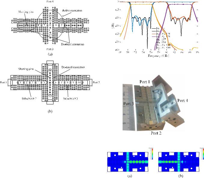
We have used three subcircuits to calculate all the dimensions of the proposed hybrid diplexer-splitter in Fig. 4. Subcircuit 1 consists of resonators 0, 4–7, and 11–14, which includes the divider section and two cavities from each channel, as shown in Fig. 6(a). The rest of the resonators are detuned by having shorting pins at their centers. In the subcircuits 2 and 3 [see Fig. 6(b)], the remaining cavities for each filter are contained in the circuits. It is important to note that subcircuits 2 and 3 can be solved at the same time because they are isolated from each other by the detuned cavities between them. Subcircuits are chosen in a way that they have an overlap with each other. This is done intentionally to consider the loading effect on the last resonator of each. This is
Fig. 8. Fabricated diplexer.
Fig. 9. Simulated E-field within the pin texture of the proposed diplexer at
(a) 73.5 and (b) 83.5 GHz.
further explained in [30]. After calculating all the dimensions by following the procedure in [25] and [30], the electric response of the diplexer-splitter is simulated, which is shown in Fig. 7. We used the CST Microwave Studio to solve the EM model. Fig. 7 shows the response of the CM compared to the optimized EM model performance.
In order to verify the design procedure and simulations, a prototype is fabricated by the computer numerical control (CNC) milling in aluminum, as shown in Fig. 8. All the inputs of the fabricated diplexer-splitter are connected to standard WR-12 waveguide flanges. Since the height of the pins (1 mm) is smaller than the height of the standard RW (1.55 mm), we have tapered the inputs in order to reach the same height, as shown in Fig. 8. The simulated E-field distribution within the pin texture of the designed diplexer at 73.5 and 83.5 GHz is shown in Fig. 9. It can be seen that the energy is well confined within the resonators, and there is no
3788 |
IEEE TRANSACTIONS ON MICROWAVE THEORY AND TECHNIQUES, VOL. 67, NO. 9, SEPTEMBER 2019 |
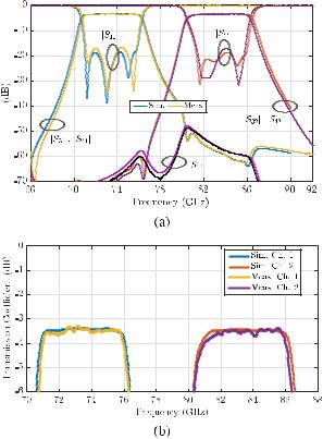
Fig. 10. (a) Measured and simulated performance of the designed diplexer.
(b) Zoomed-in view of the simulated and measured transmission coefficient of the two channels.
field leakage, in spite of no electrical contact between the pin texture and the top lid.
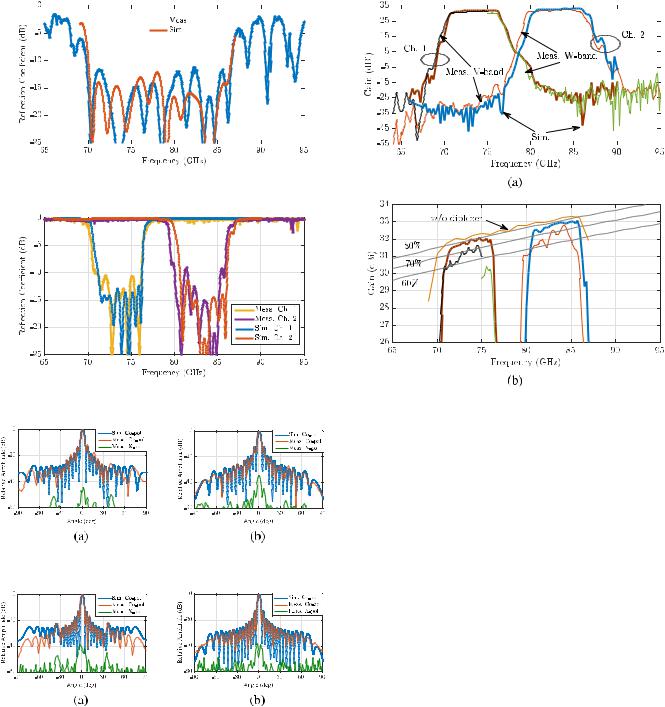
Fig. 10 shows the measured and simulated performance of the fabricated diplexer. The measured results are in a very good agreement with the simulated ones. The fabricated prototype shows a tolerance below 8 μm. The measured input reflection coefficients of the two channels are below −17 dB. The measured isolation between the two input ports (|S12|) is smaller than 50 dB. The measured isolation between the two channels (|S j 1| and |S j 2|) is also better than 50 dB. Fig. 10(b) shows that the designed diplexer has a low-loss performance. The measured transmission coefficients of both channels are better than −3.5 dB, which, in an ideal lossless situation, should be −3 dB, taking into account the power splitter for the feed network. Therefore, the fabricated prototype shows a maximum of 0.5-dB insertion loss. We remark that in the simulated results, aluminum is used for modeling the structure.
IV. ANTENNA DESIGN
We have designed a planar array antenna to provide a compact structure and high directivity. We have previously presented several gap waveguide-based slot array antennas in different frequency bands in [12], [14], [16], and [25]. The radiating element of the array and the design procedure are similar to the mentioned references. In this section, we give an overview of the designed slot array and diplexer and antenna integration, followed by experimental verifications.
Fig. 11 shows the configuration of the designed array antenna. It consists of 16 × 16 uniformly excited slots that provide a gain higher than 31 dBi in the 71–86-GHz frequency band. The array antenna shown in Fig. 11(a) is formed by four stacked up layers, where the layers do not need any electrical contact among them. A 2×2 cavity-backed slot element is used as a subarray to provide enough space to design a corporate feed network, as shown in Fig. 11(b). The designed array contains 8 × 8 subarrays in total. The slots placed on layer 4, i.e., the radiating layer, are fed by cavities on layer 3, as shown in Fig. 11(a). An RGW feed network on the backside of layer 3 feeds the cavities via coupling apertures. The configuration of the designed feed network is shown in Fig. 11(c). The feed network is divided into two parts, where each of them excites half of the radiating slots. The reason for this is that the designed array is going to be integrated with a diplexer that provides the first power division stage in order to achieve a compact integration. For the purpose of testing the array antenna separately, we have designed a GGW power divider, as shown in Fig. 11(d). This is made just for performance evaluation, and this layer will be later replaced by the designed diplexer-splitter.
Since the presented antenna has a multilayer architecture, low-loss interconnection and transitions are needed. Fig. 12 shows the two designed transitions used as interconnections of the different layers. The geometry of the proposed vertical transition between an RW and a GGW is shown in Fig. 12(a). A 90◦ E-plane bend is formed by a metal step at the end of the GGW line. This transition is used to couple the energy from the diplexer-splitter to the upper layer, where the feed network of the array antenna is located. Fig. 12(b) illustrates the transition from an RW to an RGW to match the TE10 dominant mode of the RW to the quasi-TEM mode of the RGW. The simulated S-parameters of the proposed transitions after optimization are presented in Fig. 13. Both transitions show a wideband impedance matching performance with reflection coefficients below −20 dB over the frequency band of 65–90 GHz. The dimensions of the designed array antenna are presented in Table II. It is worthy to mention that we have used bigger pins with larger periodicity in the diplexer/GGW transition layer to simplify the fabrication.
Fig. 14 shows a fabricated prototype of the integrated antenna-diplexer manufactured by CNC milling in aluminum. The layers are assembled and kept in place by using a few screws. The antenna-diplexer prototype has two WR-12 standard flanges at the backside. The layer 2 (diplexer layer) in Fig. 14 is replaced by the fabricated GGW power divider layer that is shown in Fig. 11(d), in order to verify the performance of the antenna alone as well.
The simulated and measured input reflection coefficients of the designed 16 × 16 slot array antenna are presented in Fig. 15, showing a good agreement between simulations and measurements. The measured reflection coefficient is below −11.5 dB in a frequency band of 70–86.5 GHz, which shows a broad impedance bandwidth of 21%. The antenna is measured with a waveguide input port at the bottom, as shown in Fig. 11(d).
VOSOOGH et al.: COMPACT INTEGRATED FULL-DUPLEX GAP WAVEGUIDE-BASED RADIO FRONT END |
3789 |
||||||||||||||||||||||||
|
|
|
|
|
|
|
|
|
|
|
|
|
|
|
|
|
|
|
|
|
|
|
|
|
|
|
|
|
|
|
|
|
|
|
|
|
|
|
|
|
|
|
|
|
|
|
|
|
|
|
|
|
|
|
|
|
|
|
|
|
|
|
|
|
|
|
|
|
|
|
|
|
|
|
|
|
|
|
|
|
|
|
|
|
|
|
|
|
|
|
|
|
|
|
|
|
|
|
|
|
|
|
|
|
|
|
|
|
|
|
|
|
|
|
|
|
|
|
|
|
|
|
|
|
|
|
|
|
|
|
|
|
|
|
|
|
|
|
|
|
|
|
|
|
|
|
|
|
|
|
|
|
|
|
|
|
|
|
|
|
|
|
|
|
|
|
|
|
|
|
|
|
|
|
|
|
|
|
|
|
|
|
|
|
|
|
|
|
|
|
|
|
|
|
|
|
|
|
|
|
|
|
|
|
|
|
|
|
|
|
|
|
|
|
|
|
|
|
|
|
|
|
|
|
|
|
|
|
|
|
|
|
|
|
|
|
|
|
|
|
|
|
|
|
|
|
|
|
|
|
|
|
|
|
|
|
|
|
|
|
|
|
|
|
|
|
|
|
|
|
|
|
|
|
|
|
|
|
|
|
|
|
|
|
|
|
|
|
|
|
|
|
|
|
|
|
|
|
|
|
|
|
|
|
|
|
|
|
|
|
|
|
|
|
|
|
|
|
|
|
|
|
|
|
|
|
|
|
|
|
|
|
|
|
|
|
|
|
|
|
|
|
|
|
|
|
|
|
|
|
|
|
|
|
|
|
|
|
|
|
|
|
|
|
|
|
|
|
|
|
|
|
|
|
|
|
|
|
|
|
|
|
|
|
|
|
|
|
|
|
|
|
|
|
|
|
|
|
|
|
|
|
|
|
|
|
|
|
|
|
|
|
|
|
|
Fig. 11. Designed multilayer 16 × 16 slot array antenna. (a) Different layers’ configuration. (b) 2 × 2 cavity-backed slot subarray. (c) Distribution RGW feed network. (d) Bottom layer power divider for experimental evaluation of the designed array.
TABLE II
DIMENSIONS OF THE DESIGNED ARRAY ANTENNA
(SEE TO FIGS. 11 AND 12)
Fig. 12. Configuration of the proposed (a) GGW to RW and (b) RGW to
RW transitions.
Fig. 13. Simulated performance of the designed transitions. (a) GGW to RW transition. (b) RGW to RW transition.
Fig. 14. Fabricated antenna-diplexer prototype.
Fig. 16 shows the simulated and measured reflection coefficients of the manufactured integrated antenna-diplexer. There is a certain discrepancy in the measured results with respect to the simulations. The measured input reflection coefficient of the upper channel (81–86 GHz) shows a wider passband bandwidth. This could be due to assembly errors since the
fabricated diplexer layer prototype was slightly bent because of mechanical tensions in the fabrication process. Due to the large surface of this layer, the flatness of the layers cannot be guaranteed by a few screws. However, this is not a problem
3790 |
|
|
|
|
|
|
|
|
IEEE TRANSACTIONS ON MICROWAVE THEORY AND TECHNIQUES, VOL. 67, NO. 9, SEPTEMBER 2019 |
||||||||||
|
|
|
|
|
|
|
|
|
|
|
|
|
|
|
|
|
|
|
|
|
|
|
|
|
|
|
|
|
|
|
|
|
|
|
|
|
|
|
|
|
|
|
|
|
|
|
|
|
|
|
|
|
|
|
|
|
|
|
|
|
|
|
|
|
|
|
|
|
|
|
|
|
|
|
|
|
|
|
|
|
|
|
|
|
|
|
|
|
|
|
|
|
|
|
|
|
|
|
|
|
|
|
|
|
|
|
|
|
|
|
|
|
|
|
|
|
|
|
|
|
|
|
|
|
|
|
|
|
|
|
|
|
|
|
|
|
|
|
|
|
|
|
|
|
|
|
|
|
|
|
|
|
|
|
|
|
|
|
|
|
|
|
|
|
|
|
|
|
|
|
|
|
|
|
|
|
|
|
|
|
|
|
|
|
|
|
|
|
|
|
|
|
|
|
|
|
|
|
|
|
|
|
|
|
|
|
|
|
|
|
|
|
|
|
|
|
|
|
|
|
|
|
|
|
|
|
|
|
|
|
|
|
|
|
|
|
|
|
|
|
|
|
|
|
|
|
|
|
|
|
|
|
|
|
|
|
|
|
|
|
|
|
|
|
|
|
|
|
|
|
|
|
|
|
|
|
|
|
|
|
|
|
|
|
|
|
|
|
|
|
|
|
|
|
|
|
|
|
|
Fig. 15. Comparison of measured and simulated input reflection coefficient of the designed 16 × 16 slot array.
Fig. 16. Measured and simulated performance of the integrated antennadiplexer.
Fig. 17. Simulated and measured radiation patterns of the fabricated antennadiplexer at center of channel 1 at 73.5 GHz. (a) E-plane. (b) H -plane.
Fig. 18. Simulated and measured radiation patterns of the fabricated antennadiplexer at center of channel 2 at 83.5 GHz. (a) E-plane. (b) H -plane.
in smaller workpieces, such as the fabricated diplexer in Section III.
The far-field radiation performance of the fabricated antenna-diplexer is measured in a far-field anechoic chamber. The simulated and measured radiation patterns of the fabricated antenna-diplexer are presented in Figs. 17 and 18 at the center frequencies of the two channels. As can be seen, the simulated and experimental results are in a good agreement. The fabricated prototype shows good copolar radiation patterns in E- and H -planes with a measured cross
Fig. 19. (a) Simulated and measured gains of the fabricated antenna-diplexer.
(b) Zoomed-in view of the simulated and measured gains. The dashed lines are the directivities with 80%, 70%, and 60% aperture efficiencies.
polarization better than −35 dB. Figs. 17 and 18 demonstrate that although the designed antenna has a multilayer architecture with several interconnections and transitions, the radiating slots are excited correctly.
Fig. 19 shows the simulated and measured gains of the two inputs (as illustrated in Fig. 14) of the manufactured antennadiplexer. The measurement is done with two V- and W-bands measurement setup to cover the frequency band of interest. The measured results show 55and 50-dB isolation in the gain in the 71–76- and 81–86-GHz frequency bands, respectively. A more detailed measured and simulated gain performance of the fabricated antenna-diplexer and the simulated gain of the array antenna without the diplexer is illustrated in Fig. 19(b). The maximum directivity from an aperture with the same aperture size of the designed antenna with different efficiencies is also presented in Fig. 19(b). The simulated antenna without the diplexer shows 80% antenna efficiency. The measured integrated antenna-diplexer shows average 31and 32-dB gains in channels 1 and 2 at 71–76 and 81–86 GHz, respectively, with an antenna efficiency of around 65%. It is expected that 0.5-dB [as shown in Fig. 10(b)] drop in the gain and having lower antenna efficiency is due to the extra loss of the diplexer.
V. PCB CARRIER BOARD DESIGN
Fig. 20 shows the designed PCB board to mount the Tx and Rx MMICs and supply the required dc bias voltages. The Tx and Rx dies are attached and wire bonded to the board, as shown in Fig. 20. To minimize the effect of the wire-bond and reduce the losses, we used a matching section at the RF
VOSOOGH et al.: COMPACT INTEGRATED FULL-DUPLEX GAP WAVEGUIDE-BASED RADIO FRONT END |
3791 |
|||||||||||||||
|
|
|
|
|
|
|
|
|
|
|
|
|
|
|
|
|
|
|
|
|
|
|
|
|
|
|
|
|
|
|
|
|
|
|
|
|
|
|
|
|
|
|
|
|
|
|
|
|
|
|
|
|
|
|
|
|
|
|
|
|
|
|
|
|
|
|
|
|
|
|
|
|
|
|
|
|
|
|
|
|
|
|
|
|
|
|
|
|
|
|
|
|
|
|
|
|
|
|
|
|
|
|
|
|
|
|
|
|
|
|
|
|
|
|
|
|
|
|
|
|
|
|
|
|
|
|
|
|
|
|
|
|
|
|
|
|
|
|
|
|
|
|
|
|
|
|
|
|
|
|
|
|
|
|
|
|
|
|
|
|
|
|
|
|
|
|
|
|
|
|
|
|
|
|
|
|
|
|
|
|
|
|
|
|
|
|
|
|
|
|
|
|
|
|
|
|
|
|
|
|
|
|
|
|
|
|
|
|
|
|
|
|
|
|
|
|
|
|
|
|
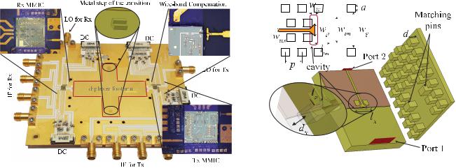
Fig. 20. Carrier board consisting of Tx and Rx MMICs, wire-bond compensation, IF and LO coaxial ports, and microstrip to GGW transitions.
Fig. 21. |
Microstrip |
to GGW transition geometry. (ltc |
= 2.57 |
mm, |
wtc = 0.62 mm, dtc |
= 0.76 mm, wg = 3.1 mm, wtm |
= 2.34 mm, |
||
w p = 1 |
mm, lp = 0.33 mm, ltm = 1.2 mm, a = 0.65 mm, d = 1 mm, |
|||
and p = 1.26 mm.) |
|
|
|
|
input/output of Rx/Tx MMICs to compensate the inductance of the wire-bond. We have used the LCP substrate that provides a stable dielectric constant and low-loss tangent at millimeterwave frequency. The substrate consists of 50-μm Rogers Ultralam 3850HT and 50-μm Rogers Ultralam 3908 bonding film on a 1-mm copper plate. The PCB is gold plated afterward to be able to apply wire-bonding. In [32] and [33], the electrical properties of LCP substrate are measured and estimated with a dielectric constant of 3.2 and a loss tangent of around 0.005 at 80 GHz. We have used these values in the modeling and all simulations.
The Tx and Rx MMICs have direct conversion architecture with differential IQ mixer based on GaAs technology. Differential IF (0–12 GHz) inputs/outputs and LO inputs (11.8–14.3 GHz) are provided with coaxial interfaces. The length of the microstrip lines that are connecting the IF coaxial connectors to the MMICs are equal to 90 and 42 mm for Tx and Rx, respectively. Furthermore, the LO path for the Tx and Rx MMICs are 35and 47-mm long, respectively. The measured insertion losses of a 50microstrip line at 3 and 15 GHz in [32] are estimated to be around 0.01 and 0.04 dB/mm, respectively. Therefore, the maximum loss of 1.88 dB is expected for the Rx LO line (largest microstrip line at a higher frequency) at 15 GHz.
The LCP dielectric is removed around the footprint of the diplexer, which is on the next layer of the module as explained earlier. The carrier board also includes the two metal steps of the GGW to RW transitions (see Fig. 12). The arrangement of the different parts of the designed carrier board is illustrated in Fig. 20. In this section, the detailed design of the main building blocks of the carrier board, such as a transition from the microstrip line to GGW and a compensation network for wire-bond interconnection, is presented. Moreover, the performance of the packaged Tx and Rx MMICs is also evaluated.
A. Microstrip to GGW Transition Design
Fig. 21 shows the designed transition between a microstrip line to the GGW. Similar transitions with different arrangement are presented in [34] and [35] at V- and W-bands, respectively.
The proposed transition is formed in two distinct parts, where the energy from the microstrip line couples to the GGW via a resonant cavity. The GGW line is created by a pin texture on the upper layer and a lid on the lower layer. The substrate is LCP ( r = 3.2) with the thickness of 100 μm. An E-plane probe is extended into the cavity, and the quasiTEM mode of the microstrip is matched to TE10 mode of GGW by using the resonant characteristic of the cavity. The length of the cavity is around λg /2 at the lower operating frequency (70 GHz). The cavity has been made within the 1-mm-thick copper plate. The copper plate acts as the ground plane of the microstrip line and the top lid of GGW. Two pins in the upper layer with a distance of around λg /4 at the lower operating frequency from the E-plane probe are extended into the waveguide channel in order to add an extra reflection and improve the impedance matching of the transition. The dimensions of the cavity, the position of the E-plane probe, and the position and length of the matching pins are optimized to achieve a broadband impedance matching. The detailed geometry of the transition is illustrated in Fig. 21 with the optimized parameter values.
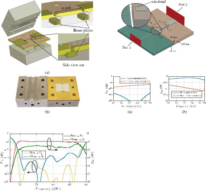
A back-to-back transition is fabricated in order to verify the performance of the designed transition. Fig. 22 shows the geometry of the back-to-back transition and the fabricated prototype. The pin texture in the upper layer, which forms the GGW line, is fabricated in aluminum with CNC machining. An 8-mm-long microstrip line is fabricated on the 100-μm LCP substrate with a 1-mm-thick copper base. To simplify the fabrication, the cavities are realized by first making through holes with the required dimensions in the 1-mm-copper plate, and afterward, the holes are closed from the backside with small metal pieces. We have used brass pieces and conductive silver paste to enclose the holes and form the cavities, as shown in Fig. 22(a).
The simulated and measured performance of the fabricated back-to-back transition is shown in Fig. 23. The measured reflection coefficient is below −12 dB over the frequency band 69–87 GHz. The fabricated prototype shows higher insertion loss than the simulation. A measured average insertion loss
3792 |
IEEE TRANSACTIONS ON MICROWAVE THEORY AND TECHNIQUES, VOL. 67, NO. 9, SEPTEMBER 2019 |
Fig. 22. (a) Configuration of back-to-back transition between the microstrip line and GGW. (b) Fabricated back-to-back microstrip to the GGW transition prototype.
Fig. 24. Configuration of the compensation matching network for wire-bond
interconnection. (lcop1 = 0.48 mm, wcop1 = 0.09 mm, lcop2 = 0.49 mm, and wcop2 = 0.1 mm.)
Fig. 25. Simulated S-parameters of wire-bonded 50-μm microstrip lines in GaAs and LCP substrates with and without compensation. (a) Reflection coefficient. (b) Transmission coefficient.
Fig. 23. Simulated and measured performance of the back-to-back microstrip to GGW transition.
of 1.5 dB (including the losses in the 8-mm microstrip line) has been achieved over the frequency band 71–86 GHz, where the simulated insertion loss is 1 dB over the same frequency band. The extra loss could be due to the enclosure of the cavities with conductive silver paste and extra substrate losses. The measured results in [32] shows that the insertion loss of a 50microstrip line on a 100-μm LCP substrate is around 0.11 dB/mm at 80 GHz. Therefore, by subtracting the loss of the 8-mm microstrip line of the fabricated back-to-back transition, the measured insertion loss of a single transition is estimated to be around 0.31 dB.
B. Wire-Bond Compensation Network for TX/RX MMIC to Board Interconnection
Wire bonding is a conventional interconnection approach to electrically connect the MMIC to microstrip or coplanar
waveguide (CPW) transmission lines. However, using this approach becomes tricky by increasing the operating frequency. The wire-bond introduces an extra inductance that needs to be compensated in order to achieve a proper impedance matching, especially at high frequencies. Fig. 24 shows the matching section that we have used to compensate for the wire-bond effect. A T-shaped microstrip section with a capacitive impedance is used to compensate the inductance that is introduced by wire-bonding. We have assumed that a 50microstrip line on a 50-μm GaAs substrate (εr = 12.5) is connected to a microstrip line on a 100-μm substrate with a dielectric constant of 3.25 by a low profile wire-bond. The simulated S-parameters with and without compensation are presented in Fig. 25. The materials are considered lossless, and the losses in Fig. 25(b) are only due to mismatch and radiation losses. Fig. 25(a) shows that the reflection coefficient improves from around −8 dB to below −15 dB over the frequency band 70–88 GHz by using the compensation matching network.
C. Tx and Rx Modules Performance
The performance of the Tx and Rx MMICs is measured to characterize and evaluate the packaging and assembly. The measurement setup is shown in Fig. 26. The IF and LO are provided by a Keysight N5241A PNA-X network analyzer and RF input/output is connected to a VDI WR-12 extender. The IF port from the network analyzer is connected to a 180◦ hybrid coupler that provides two out-of-phase outputs with equal amplitude. The outputs of the 180◦ hybrid are connected to two 90◦ hybrid couplers to provide differential IQ for input/output of Tx/Rx modules. An extra part with a GGW line is also