

диафрагмированные волноводные фильтры / f132e880-957c-4b4f-9cee-ff39aca1584f
.pdfThis article was downloaded by: [Simon Fraser University] On: 11 November 2014, At: 23:38
Publisher: Taylor & Francis
Informa Ltd Registered in England and Wales Registered Number: 1072954 Registered office: Mortimer House, 37-41 Mortimer Street, London W1T 3JH, UK
Journal of Electromagnetic Waves and Applications
Publication details, including instructions for authors and subscription information: http://www.tandfonline.com/loi/tewa20
A Millimeter-Wave E-Plane Bandpass Filter using Multilayer Low Temperature Co-Fired Ceramic (LTCC) Technology
Z. Wang a , X. Zeng b , B. Yan c , R. Xu d & W. Lin e
aSchool of Electronic Engineering, University of Electronic Science and Technology of China, Chengdu, Sichuan 610054, China
bSchool of Electronic Engineering, University of Electronic Science and Technology of China, Chengdu, Sichuan 610054, China
cSchool of Electronic Engineering, University of Electronic Science and Technology of China, Chengdu, Sichuan 610054, China
dSchool of Electronic Engineering, University of Electronic Science and Technology of China, Chengdu, Sichuan 610054, China
eSchool of Electronic Engineering, University of Electronic Science and Technology of China, Chengdu, Sichuan 610054, China
Published online: 03 Apr 2012.
To cite this article: Z. Wang , X. Zeng , B. Yan , R. Xu & W. Lin (2010) A MillimeterWave E-Plane Band-pass Filter using Multilayer Low Temperature Co-Fired Ceramic (LTCC) Technology, Journal of Electromagnetic Waves and Applications, 24:1, 71-79, DOI: 10.1163/156939310790322091
To link to this article: http://dx.doi.org/10.1163/156939310790322091
PLEASE SCROLL DOWN FOR ARTICLE
Taylor & Francis makes every effort to ensure the accuracy of all the information (the “Content”) contained in the publications on our platform. However, Taylor

Downloaded by [Simon Fraser University] at 23:38 11 November 2014
& Francis, our agents, and our licensors make no representations or warranties whatsoever as to the accuracy, completeness, or suitability for any purpose
of the Content. Any opinions and views expressed in this publication are the opinions and views of the authors, and are not the views of or endorsed by Taylor & Francis. The accuracy of the Content should not be relied upon and should be independently verified with primary sources of information. Taylor and Francis shall not be liable for any losses, actions, claims, proceedings, demands, costs, expenses, damages, and other liabilities whatsoever or howsoever caused arising directly or indirectly in connection with, in relation to or arising out of the use of the Content.
This article may be used for research, teaching, and private study purposes. Any substantial or systematic reproduction, redistribution, reselling, loan, sublicensing, systematic supply, or distribution in any form to anyone is expressly forbidden. Terms & Conditions of access and use can be found at http:// www.tandfonline.com/page/terms-and-conditions

Downloaded by [Simon Fraser University] at 23:38 11 November 2014
J. of Electromagn. Waves and Appl., Vol. 24, 71–79, 2010
A MILLIMETER-WAVE E-PLANE BAND-PASS FILTER USING MULTILAYER LOW TEMPERATURE CO-FIRED CERAMIC (LTCC) TECHNOLOGY
Z. Wang, X. Zeng, B. Yan, R. Xu, and W. Lin
School of Electronic Engineering
University of Electronic Science and Technology of China Chengdu, Sichuan 610054, China
Abstract—This paper presents a substrate integrated waveguide (SIW)-based millimeter-wave E-plane band-pass filter (BPF) with multilayer Low Temperature Co-fired Ceramic (LTCC) technology. The vertical metal walls of SIW and metal fins of the evanescent waveguides are realized by closely spacing metallic via-holes. A threeorder Chebyshev E-plane BPF is developed and verified by full-wave simulation. The proposed filter is fabricated using LTCC technology, and a tapered line is designed as the transition between the SIW and microstrip line. Good agreement between simulated and measured results is observed.
1. INTRODUCTION
E-plane metal insert technology is a conventional cost-e ective implementation of direct-coupled cavity filters, and their ease of manufacturing and availability through accurate design software have made E-plane filter widely employed in several microwave and millimeter-wave applications for over 20 years [1, 2]. But, despite their favorable characteristics, classical E-plane rectangular waveguide filters are of large size, heavy weight, high cost, and also not easy to be integrated with planar circuit technology, being a 3-D structure. Recently, a new planar waveguide structure called substrate integrated waveguide (SIW) was proposed [3–5, 18] to fabricate an equivalent rectangular waveguide using standard PCB process, thick-film process or LTCC process. Such a class of waveguides has the advantages of high Q-factor, low insertion loss, low cost, etc. It can be easily integrated
Corresponding author: Z. Wang (wangzhigang19791@163.com).
Downloaded by [Simon Fraser University] at 23:38 11 November 2014
72 |
Wang et al. |
into microwave and millimeter-wave integrated circuits, also suits the realization of high performance band-pass filters at microwave and millimeter-wave frequency band. Besides, the theoretical investigation of the guidedand leaky-wave characteristics of SIW was presented, and the empirical formulas of calculating the equivalent rectangular waveguide width were developed to provide a valuable design criterion for implementing SIW [6]. Several SIW-based cavity filters have been realized on flip-chip modules [7], printed circuit board [8–11, 15–17], and thick-film technology [12]. With the mature multilayer technology, SIW filters are also fabricated using LTCC technology [13, 14]. LTCC technology provides significant benefits in terms of design flexibility and density.
In this paper, a SIW-based millimeter-wave E-plane BPF is developed using multilayer LTCC technology. By following the design criterion and empirical formulas [13], we could have the equivalent closed rectangular waveguide structure parameters. The vertical metal walls of substrate integrated waveguide (SIW) and metal fins of the waveguide resonators are realized by closely spaced metallic via-holes. A three-order Chebyshev E-plane BPF is developed and verified by full-wave simulation. The proposed filter is fabricated using multilayer LTCC technology, and a tapered line is designed as the transition between the SIW and microstrip line. Good agreement between simulated and measured results is observed.
2. DESIGN OF THE SIW E-PLANE METAL FINS BAND-PASS FILTER
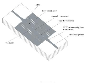
The configuration of the proposed SIW E-plane band-pass filter is shown in Fig. 1. The filter consists of three SIW resonators and tapered microstrip line transition that connects a 50 Ω microstrip line and SIW on the same dielectric substrate. The SIW structure is realized by incorporating two lines of closely spaced metallic via-holes in a substrate with metallic top and bottom surfaces, and the metal fins of the waveguide resonators are formed by closely spaced via-holes. In this way, planar and non-planar can be integrated together on the same substrate.
The operating mechanism of the SIW is quite similar to that of a conventional rectangular waveguide, except that only TEmo modes can exit in SIW. Therefore, cut-o frequency of the SIW modes are simply calculated as follows [3, 4]:
fCmn = 2π√με |
ae |
2 |
+ b |
|
(1) |
||
1 |
|
|
mπ |
|
nπ |
2 |
|
Millimeter-wave E-plane BPF using LTCC technology |
73 |
Downloaded by [Simon Fraser University] at 23:38 11 November 2014
Figure 1. Configuration of the proposed SIW E-plane band-pass filter.
fC10 = |
1 |
(2) |
2ae √με |
where ae is the e ective width of the SIW, approximately given by a − Ø21/0.95 · p; Ø1 is the diameter of the metallic via-holes of the SIW; a and b are the width and height of the SIW, respectively; p is the space between metallic via-holes; ε is the relative permittivity of the LTCC substrate. The SIW width a is calculated by the cut-o frequency of the TE10 waveguide mode. The pitch p and diameter Ø1 of metallic via-holes are determined to minimize the leakage loss of the SIW. Metallic via-holes arrays of the diameter Ø2 are used to form metal fins. By considering manufacturing limits of LTCC technology and insertion loss, the parameters of the SIW are selected as follows:
a = 2.8 mm, Ø1 = 0.21 mm, Ø2 = 0.13 mm, p = 0.5 mm, b = 0.376 mm, and the selected height b of the SIW is just the thickness of the four
layers LTCC substrate Ferro-A6M.
Design of a transmission line transition requires simultaneous matching of the fields and impedance. Several transition designs have been reported [5, 8]. Usually the transition is implemented by SIWmicrostrip line or SIW-CPW. In this paper, the tapered microstrip line is selected as the I/O ports transition between the SIW and microstrip, due to its simple structure, easy fabrication and good performance. It is easy to achieve a fairly good field matching by their dominant vertical E-field components. Their impedance is also matched using the

74 |
Wang et al. |
Downloaded by [Simon Fraser University] at 23:38 11 November 2014
Figure 2. Layout of the SIW E-plane band-pass filter.
tapered microstrip line without significant disturbance of their vertical E-field components. A commercial full-wave 3-D FEM simulator (Ansoft HFSS) is used to analyze and optimize the transition structure, L = 1.3 mm, and W1 = 1 mm are obtained.
The layout of the proposed SIW E-plane band-pass filter with microstrip line I/O ports is shown in Fig. 2. The filter is composed of three SIW resonators with a half-wavelength and microstrip line to SIW transitions at both ends of the SIW. In order to design the filter, the K-inverters between ith and jth resonator are calculated as follows [19]:
K01 = Kn,n+1 = |
|
|
2g0g1 |
|
|
|
|
(3) |
|
|
|
πF BW |
|
|
|
|
|||
|
|
|
|
|
|
|
|
||
Ki,i+1 |i=1 to n−1 = |
2 |
|
|
|
gigi+1 |
(4) |
|||
|
|
|
πF BW |
1 |
|
|
|||
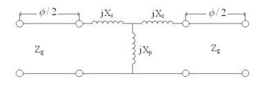
where gis are the element values of Chebyshev lowpass prototype filter; FBW is the fractional bandwidth; n is the order of the filter. The values of the K-inverters are controlled by changing the length of gij of a array of metallized via-holes with an identical diameter of 0.13 mm inside the SIW. The evanescent waveguide can be represented with an impedance inverter (K-inverter) circuit, as shown in Fig. 3. Normalized inverter values K and negative electrical length φ are given by [19]:
Zg |
= tan −2 tan−1 |
|
|
Zg |
+ |
|
Zg |
+ 2 tan−1 |
Zg |
|
(5) |
||||||||||||
K |
|
|
|
1 |
|
|
|
|
|
2X p |
|
|
Xs |
|
1 |
|
Xs |
|
|
||||
|
|
|
|
1 |
|
2X p |
|
|
Xs |
|
|
|
|
1 Xs |
|
|
|
|
|||||
φ = |
|
tan− |
|
|
|
+ |
|
|
|
|
tan− |
|
|
|
|
|
|
|
(6) |
||||
|
Zg |
Zg − |
|
Zg |
|
|
|||||||||||||||||
|
|
− |
|
|
|
|
|
|
|
|
|
|
|
||||||||||
where Zg is a wave impedance of SIW.
Millimeter-wave E-plane BPF using LTCC technology |
75 |
Downloaded by [Simon Fraser University] at 23:38 11 November 2014
Figure 3. Impedance inverter (K-inverter) circuit for evanescent waveguide.
By parameter extraction and the help of simulator, the relations between the normalized inverter value (K/Zg ) and the length (gij ) of fin and between negative electrical length φ and gij can be confirmed using the equivalent circuit of evanescent waveguide and Equations (5) and (6). The length of the half-wavelength resonators is given by [19]:
Ln = |
2π |
π + |
2 |
(φj + φj+1) |
(7) |
|
λg0 |
|
1 |
|
|
Thus, the initial physical parameters of filter can be determined. Finally, a commercial full-wave 3-D FEM simulator Ansoft HFSS is used to analyze and optimize the filter after the initial design.
Using K-inverter values calculated by (3) and (4), a 0.1 dB ripple three order Chebyshev band-pass filter with a 1 GHz bandwidth centered at 37.8 GHz is designed. Based on well-known filter synthesis technique, the element values of Chebyshev lowpass prototype filter is
found to be: g0 = 1.0000, g1 = 0.8794, g2 = 1.1132, g3 = 0.8794, g4 = 1.0000, K01 and K34 is 0.2829, and K12 and K23 is 0.0711. According to the calculated results, the lengths g01 = g34 = 0.3 mm
and g12 = g23 = 1.2 mm are obtained. A commercial full-wave 3-D FEM simulator (Ansoft HFSS) is used to analyze and optimize the filter after the initial design.
3. MEASURED RESULTS
To verify the proposed SIW E-plane band-pass filter, the 0.1 dB ripple three order Chebyshev band-pass filter with a 1 GHz bandwidth centered at 37.8 GHz is fabricated. The filter was fabricated in a fourteen-layer Ferro A6-M LTCC substrate, of which the relative permittivity is about 5.3 at 37 GHz; the loss tangent is 0.003; the thickness of each layer is 0.094 mm. Only the upper four layers were used, another ten layers were stacked to fit with other configurations.
76 |
Wang et al. |
Downloaded by [Simon Fraser University] at 23:38 11 November 2014
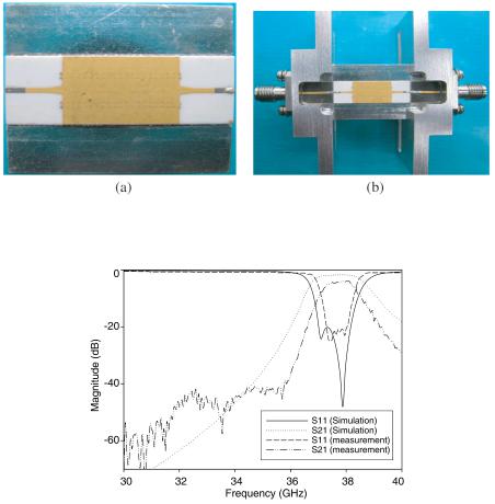
Figure 4. Photograph of the SIW E-plane band-pass filter (a) top view, (b) whole device with test fixture.
Figure 5. Simulated and measured S parameters of the proposed SIW E-plane bandpass filter.
The metallic part was fabricated by gold. Photograph of the filter is shown in Fig. 4. Compared with conventional rectangular waveguide BPF, it is so compact that the filter dimensions are only 20 × 8 × 0.376 mm3 (including the tapered microstrip line transitions of I/O ports), and could be used in modules directly without any additional transitions.
The manufactured prototype of the filter was measured using Agilent E8363B vector network analyzer. For measuring expediently, a pair of test fixtures was connected at the I/O ports of the filter as shown in Fig. 4. The simulated and measured S-parameters of the filter are
Downloaded by [Simon Fraser University] at 23:38 11 November 2014
Millimeter-wave E-plane BPF using LTCC technology |
77 |
shown in Fig. 5. It can be seen from Fig. 5 that the operated bandwidth of measurement results is little smaller than that of simulation results, and insertion loss is larger. These could be attributed to tolerance of manufacture and relativity permittivity, material and radiation loss. In spite of these, the full-wave EM simulation (HFSS) and measurement results still have a good agreement. The measured minimum insertion loss is about 3.7 dB (including the tapered microstrip line transitions of I/O ports) at 37.9 GHz. From 37.3 GHz to 38.1 GHz, the insertion loss is less than 5 dB, and the return loss is better than 17 dB. The measured out of band rejection is better than 40 dB and 28 dB at 2 GHz lower and higher separation from a center frequency 37.8 GHz, respectively.
4. CONCLUSION
In this paper, a SIW E-plane metal fins band-pass filter with tapered microstrip line transition has been designed, fabricated and measured. According to validation, measured results are in good agreement with simulated ones. From 37.3 GHz to 38.1 GHz, the insertion loss is less than 5 dB, and the return loss is better than 17 dB. The measured out of band rejection is better than 40 dB and 28 dB at 2 GHz lower and higher separation from a center frequency 37.8 GHz, respectively. The filter dimensions are only 20 × 8 × 0.376 mm3 (including the tapered microstrip line transitions of I/O ports) and could be used in modules directly without any additional transitions.
ACKNOWLEDGMENT
This work is supported by National Nature Science Foundation of China under Grants 60671028, 60701017, and 60876052.
REFERENCES
1.Vahldieck, R., J. Bornemannn, F. Arndt, and D. Grauerholz, “Optimized waveguide E-plane metal insert filters for millimeter wave appplicatons,” IEEE Trans. Microw. Theory Tech., Vol. 31, No. 1, 65–69, Jan. 1983.
2.Shih, Y. C. and T. Itoh, “E-plane filters with finite-thickness septa,” IEEE Trans. Microw. Theory Tech., Vol. 31, No. 12, 1009– 1013, Dec. 1983.
3.Uchimura, H., T. Takenoshita, and M. Fujii, “Development of ‘a laminated waveguide’,” IEEE Trans. Microw. Theory Tech., Vol. 46, No. 12, 2437–2443, Dec. 1998.
Downloaded by [Simon Fraser University] at 23:38 11 November 2014
78 |
Wang et al. |
4.Deslandes, D. and K. Wu, “Integrated microstrip and rectangular waveguide in planar form,” IEEE Microw. Wireless Compon. Lett., Vol. 11, No. 2, 68–70, Feb. 2001.
5.Deslandes, D. and K. Wu, “Single-substrate integration technique of planar circuits and waveguide filters,” IEEE Trans. Microw. Theory Tech., Vol. 51, No. 2, 593–596, Feb. 2003.
6.Xu, F. and K. Wu, “Guided-wave and leakage characteristics of substrate integrated waveguide,” IEEE Trans. Microw. Theory Tech., Vol. 53, No. 1, 66–73, Jan. 2005.
7.Ito, M., K. Maruhashi, K. Ikuina, T. Hashiguchi, S. Iwanaga, and K. Ohata, “A 60-GHz-band planar dielectric waveguide filter for flip-chip modules,” IEEE Trans. Microw. Theory Tech., Vol. 49, No. 12, 2431–2436, Dec. 2006.
8.Choi, S. T., K. S. Yang, K. Tokuda, and Y. H. Kim, “A V- band planar narrow bandpass filter using a new type integrated waveguide transition,” IEEE Microw. Wireless Compon. Lett., Vol. 14, No. 12, 545–547, Dec. 2004.
9.Zhang, X. C., Z. Y. Yu, and J. Xu, “Novel band-pass substrate integrated waveguide (SIW) filter based on complementary split ring resonators (CSRRs),” Progress In Electromagnetics Research, PIER 72, 39–46, 2007.
10.Ismail, A., M. S. Razalli, M. A. Mahdi, R. S. A. R. Abdullah, N. K. Noordin, and M. F. A. Rasid, “X-band trisection substrate-integrated waveguide quasi-elliptic filter,” Progress In Electromagnetics Research, PIER 85, 133–145, 2008.
11.Wang, R., L. S. Wu, and X. L. Zhou, “Compact folded substrate integrated waveguide cavities and bandpass filter,” Progress In Electromagnetics Research, PIER 84, 135–147, 2008.
12.Stephens, D., P. R. Young, and I. D. Robertson, “Millimeter-wave substrate integrated waveguides and filters in photoimageable thick-film technology,” IEEE Trans. Microw. Theory Tech., Vol. 53, No. 12, 3832–3838, Dec. 2005.
13. Lee, J. H., S. Pinel, J. Papapolymerou, J. Laskar, and M. M. Tentzeris, “Low-loss LTCC cavity filters using systemon package technology at 60 GHz,” IEEE Trans. Microw. Theory Tech., Vol. 53, No. 12, 3817–3824, Dec. 2005.
14.Gu, J., Y. Fan, and Y. Zhang, “A X-band 3-D SICC filter with low-loss and narrow band using LTCC technology,” Journal of Electromagnetic Waves and Application, Vol. 23, No. 8–9, 1093– 1100, 2009.
15.Sotoodeh, Z., B. Biglarbegian, F. Hodjatkashani, and H. Ameri,