

диафрагмированные волноводные фильтры / 66e0dd65-ffdb-45f0-bd8d-8839d87a09d0
.pdfA Subwavelength Microwave Bandpass Filter Based
on a Chiral Waveguide
Maliheh Khatibi Moghaddam1 and Romain Fleury1
1 Laboratory of Wave Engineering, École Polytechnique Fédérale de Lausanne (EPFL), 1015 Lausanne, Switzerland romain.fleury@epfl.ch; Tel.: +41-21-69-32683
maliheh.khatibimoghaddam@epfl.ch
Abstract— Wave manipulation at a subwavelength scale has recently attracted significant interest, especially for lowfrequency wave propagation, from acoustic to microwave devices. Recently, a few methods achieving subwavelength routing using locally resonant metamaterials have been proposed, foreseeing new technologies for ultra-compact passive components, e.g. in satellite communications. In this paper, we aim at exploiting such a technique for designing a miniature microwave filter, which guides modes at the interface between two locally-resonant bang-gap materials with opposite chirality, forming a so-called chiral subwavelength waveguide. It has been recently demonstrated that such a chiral waveguide has inherent robustness against imperfections in both the position and resonance frequencies of the local resonators, which can be leveraged for realizing robust subwavelength systems. Here, we use this property in order to realize a bandpass filter, by purposely adding resonant defects to get rid of parasitic modes in the out-of-band region without perturbating the main guided mode. We demonstrate the potentiality of integrating subwavelength resonators directly into the active region of the filter for enhancing its order and suppressing spurious bands, a functionality conventionally obtained only by cascading bulky stages. Finally, we combine this approach for removing the parasitic modes with dispersion engineering methods, demonstrating a bandpass filter with improved frequency selection, as well as a high level of rejection, more than 40dB, in the out-of-band region of the filter.
Index Terms—locally resonant metamaterials, chirality, bandpass filter, subwavelength, satellite communication.
I.INTRODUCTION
Microwave passive components are conventionally realized based on transmission lines, including rectangular waveguides, coplanar waveguides, and microstrip lines [1]. In satellite communications, rectangular waveguides are key elements of passive components that have experienced many advances both from the theoretical, technological and performance standpoints [2]–[4]. Nonetheless, unlike active devices, microwave passive components have not improved significantly with regards to size reduction. This is due to the fact that the geometrical scaling in the conventional methods is generally governed by the operating frequency, prohibiting field manipulation and guiding at subwavelength (sub-λ) scales. In order to leverage spatial dispersion to guide waves
at the deep subwavelength scale, which is particularly important for microwave and acoustic devices, the promising concept of locally resonant metamaterial crystals (LRMCs) has been recently proposed [5], [6]. An LRMC is built from small spatially-local resonant inclusions, arranged periodically at the sub-λ scale. In contrary to photonic crystals, the operating frequency of an LRMC is decoupled from the periodic spatial scale and mostly depends on the resonant behavior of its constitutive elements. Hence, sub-λ focusing and waveguiding are possible, as long as the resonant inclusions are electrically small. In an LRMC, sub- λ wave localization is possible in a bandgap, known as hybridization bandgap (HBG), which opens slightly above the critical resonances [6]. Unlike the Bragg bandgaps, HBG nucleates as a result of multiple Fano scattering and mainly depends on the individual meta-atoms resonances rather than the spatial arrangement.
In this paper, we exploit an LRMC structure, composed of a lattice of resonant wires between two parallel plates (bed of nails) [7], to realize a microwave filter in the Ku band. The wire media are one of the most thoroughly studied classes of metamaterials, known for over six decades for emulating plasma behavior [8], exhibiting strong dispersive properties, even at low frequencies [9]. The potential of this structure for realizing an LRMC and various sub-wavelength guiding mechanisms, based on frequency-defect tunneling [6], [10], chirality[11] or topological edge modes[12]–[15], has also been recently demonstrated.
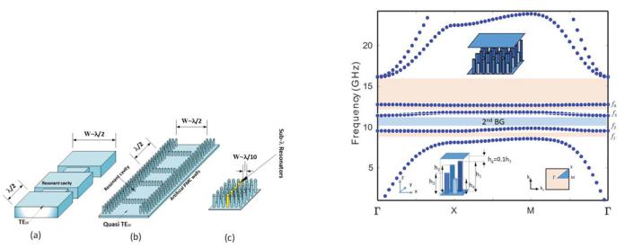
During the last decade, the structure of a bed of nails between parallel plates has been also utilized for the construction of perfect electrical conductor/perfect magnetic conductor (PEC/PMC)-walled waveguides, so-called gap waveguides (GWs), profit from low loss and packaging advantages[16]. In contrary to GWs, in which the artificial PMC walls support the propagation of the quasi TEM and quasi TE modes, the wave tunneling in LRMC-based waveguides is based on an unconventional sub-λ guided modes. Besides, the operating frequency can be adjusted, by altering the length of wires, with no necessity of changing the periodicity or defect width. Figure. 1 (a), (b), and (c) respectively show three samples of the three different
Authorized licensed use limited to: FLORIDA INTERNATIONAL UNIVERSITY. Downloaded on July 24,2020 at 14:01:50 UTC from IEEE Xplore. Restrictions apply.
technologies for realizing a microwave filter. Among the recently-proposed and experimentally-demonstrated techniques for realizing sub-λ waveguides in LRMCs, the chiral waveguide proposed in [11] has quantitatively shown more immunity to geometrical flaws and thus better management of tolerance sensitivities in comparison with the other sub-λ waveguides, have been designed based on frequency-defects [10] and topological modes [12]–[14]. A chiral waveguide exploits the interface modes occurring at the boundary between two sub-bandgap materials, composed of resonant meta-molecules with opposite chirality [11]. Due to the existence of parasitic modes, emerging in the out-of- band region, near to the passbands, this structure needs some modifications to provide acceptable filtering characteristics. Analogous to conventional microwave filters, in which the presence of spurious bands degrades the performance of the filter, here the suppression of these parasitic modes is critical, especially in certain applications that require huge rejection bandwidths such as satcom duplexers. In order to remove the obtrusive modes in conventional microwave filters, some traditional techniques have been studied, including the use of half-wavelength, short-circuits stubs, chip capacitors, cascaded stopband, or Bragg bandgap filters [17]–[20]. However, these techniques, based on cascading these components next to the filter, always increase the device area, and come with bandwidth challenge. Therefore, suppressing the spurious bands of the sub-λ waveguides, without increasing the size of the system is a non-obvious task.
In this paper, we propose a method for realizing a compact sub-λ bandpass filter from a chiral waveguide, with improved stopband response without having to increase its size. This is done by exploiting the robustness of the chiral guiding mechanism, which allows us to dope it with sub-λ resonators directly inside the active region of the structure, in order to tailor its filtering response. We demonstrate how these additions induce a sub-λ HBG that can suppress parasitic modes, without growing the size of the filter. Thus, the frequency selection of the filter is modified by tuning the length of the resonant wires, which could be realized using screws. Considering the optimal parameters, a high level of rejection, as well as an improved frequency selection, are obtained in an acceptable bandwidth.
II.RESULTS
A.Design of a Chiral Waveguide in Ku-band
Here we aim at exploiting the interface modes occurring at the boundary between two bandgap materials with similar resonant building blocks, or meta-molecules, but with opposite chirality. We initially design the meta-molecules of one of these periodic structures, shown in Fig. 2, to extract the induced bandgaps that emerge between their different resonances. Each unit cell, containing one meta-molecule, is constructed using four quarter-wavelength copper wires on a copper ground plane, and topped by another copper plane, leading to distinct individual resonance frequencies distributed around a central frequency of fc=12GHz. The resonance frequencies of metallic wires are accordingly
adjusted by f1=fc-2Δ, f2=fc- , f3=fc+Δ, f4=fc+2 , where is set at 0.1fc, inducing sufficiently large bandgaps. The wires, with a diameter of 1mm, are arranged on a subwavelength square of side c=0.1λc=2.5mm (λc is corresponding freespace wavelength at fc) and can be distributed clockwise (CW) or counterclockwise (CCW) with growing frequencies in a square lattice of period a=2c=5mm. Each basic cell in this structure interacts with propagating plane waves, through multiple Fano scattering, resulting in HBGs occurring near each of the resonance frequencies of the backbone metamolecule (noted f1, f2, f3, and f4). Therefore, the band diagram of this crystal comprises a series of propagative bands, separated by bandgaps, shown by colored regions in Fig. 2. Next, we consider modes guided at an interface between the CW and CCW crystals. According to the fact that the CW and CCW meta-molecules support the same resonant modes with opposite chirality of field distribution, the interface zone between CW and CCW structures can support localized modes in each of their common bandgaps.
Fig. 1. The schematics of three samples of microwave filters based on a) rectangular waveguides, b) GW, and c) LRMC.
Fig.2 The band diagram of the proposed LRMC, consist of the metamolecules constructed by four copper wires having distinct lengths in CCW chirality. The colored regions exhibit the band gaps above the resonance frequencies of individual atoms (f1,2,3,4). The blue region in the 2nd bandgap, we use in this paper for waveguiding.
Authorized licensed use limited to: FLORIDA INTERNATIONAL UNIVERSITY. Downloaded on July 24,2020 at 14:01:50 UTC from IEEE Xplore. Restrictions apply.
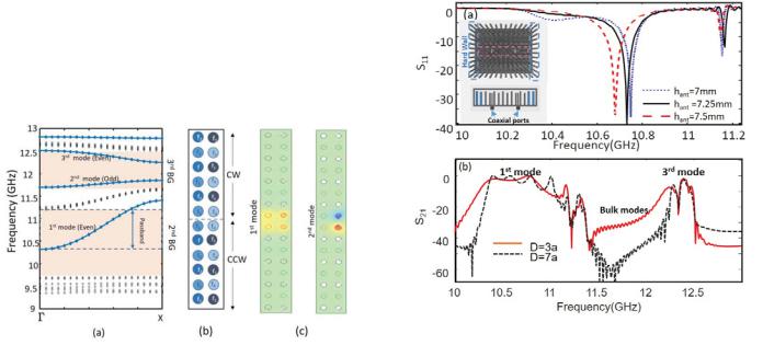
The band diagram of such a chiral waveguide formed by a crystal interface in the ΓX direction, which is obtained by considering a supercell with a size of a×6a in the xy plane (Fig. 3(a)), shows some interface-localized modes in the second and third bandgaps (solid lines), as well as the bulk modes (open circles). Looking at the field distribution of the localized modes in the bandgap, we now classify them to be of monopolar or dipolar nature (even and odd transverse symmetries). While one monopole guided-mode appears in the second bandgap, two modes with distinct symmetries exist in the third gap. As shown in Fig. 3(b), the second mode has dipolar symmetry, and hence the first monopolar mode cannot couple to it. However, coupling with the 3rd mode is possible. If we use the first monopolar mode as a basis for a filter, the third mode will create a parasitic mode in the out- of-band region, which must be suppressed.
B. Coaxial Coupling to the Chiral Waveguide
For exciting the passband in the full-wave simulation of the chiral waveguide, we employ an E-plane coaxial transition, so-called orthogonal transition, by entering the probes from cylindrical perforated coaxial ports through the bottom plate of the box, shown in Fig. 4(a). Due to the symmetry of the radiation pattern of coaxial wires, we can efficiently couple to the first mode after adjusting the radius, height, and position of the probes without adding any bulky adaptor. The two tiny probes with a diameter of 0.6mm, avoiding the generation of higher-order modes, are separated by a distance of D=3a=15mm along the waveguide. Our studies have shown that a coax wire penetrating with hp=7.25mm into the box can match well to considered guided-mode (Fig. 4(a)). In addition, to force the energy to propagate between the probes, a short-circuiting wall (socalled “back short”), need to be located at a certain distance from the probe. The back short reflects back the EM energy propagating in the wrong way towards the probe, where it interferes with the incident wave. Therefore, the distance between the back shorts and the probes should be a quarter of the wavelength (λc/4=6.25mm).
Here, the back shorts are made from artificial bandgap materials, created by inserting two rows of wires with a periodicity of c, prohibiting wave propagation in the frequency range of interest. We have checked that two layers of wires with a height hsh=7.25mm can work as a hard wall for this filter. The transfer scattering coefficient (S21) of this structure, shown in Fig. 4(b), exhibits the influence of the bulk and the third mode (the monopole mode in the third gap) in the out-of-band region of the filter. It also shows that increasing the distance between the coaxial ports (D) results in rejection of the bulk modes and inherently steeper roll-off. Although the longer distance between the ports reduces the strength of the bulk modes, it is not able to make a perfect rejection in the stopband due to the existence of the 3rd mode. In the next sections, considering the small structure (D=3a), we will propose two techniques to design of a higher-order bandpass filter, comprising the improved frequency selection and high level of rejection in the stopband.
C.High-order Chiral Filter with Improved Stopband Using Subwavelength Resonators Doping
Here, for improving the order of the system, the frequency selection, and the rejection strength, instead of increasing the distance between the ports or cascading additional segments, we propose to exploit the robustness of the guiding mechanism and dope the active region of the filter with sub- λ resonant wires (e.g. screws), essentially increasing the order of the filter (Fig. 5a). These added pins, when properly coupled to the transmission line, are able to suppress the spurious bands, relying on their induced bandgap. Their effect is equivalent to adding zeros in the out of band region of the system.
Fig. 3. a) The band diagram for a chiral waveguide in ΓX direction, the gray regions show the second and third bandgaps and the solid lines indicate the localized modes in the interface, b) The corresponding supercell, c) The mode profile of the monopole and dipole modes.
Fig. 4. a) The S11 for the two-port chiral filter inserted in a copper box for different probe sizes (hant). The inset is a schematic of the structure, the blue and pink dashed line respectively indicate the hard wall and interface zones. b) The S21 for short and long structures, showing the passband, regarding the 1st mode, and the parasitic modes (bulk and 3rd modes).
Authorized licensed use limited to: FLORIDA INTERNATIONAL UNIVERSITY. Downloaded on July 24,2020 at 14:01:50 UTC from IEEE Xplore. Restrictions apply.
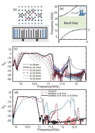
Figure 5(b) recalls the induced bandgap of a simple wire medium (h=6.1mm, a=5mm) along the propagation axis (ΓX), which could be used to suppress the parasitic modes without interfering with the waveguide functionality. Therefore, in order to obtain improved filtering properties, we investigate the effect of adding sub-λ resonant wires with different positions, resonance frequencies, and sizes. We have found that by inserting one set of three resonant wires, in the interface line with the periodicity of a=5mm and height of hi (around 6.25mm), we can reject the parasitic modes around 12GHz and enhance the frequency selection of the filter. The S21 spectra for different values of hi, shown in Fig. 5(c), demonstrates that by increasing the heights of the resonators (reducing their resonance frequency), i.e. shifting the lower edge of the bandgap to lower frequencies, improves the rejection at the expense of destroying the passband. Hence, by tuning the size of these internal pins at hi=6.1mm, a steeper roll-off can be obtained, while the rejection still has to be improved in a subsequent step. For this purpose, we employ supplemental pins adjacent to the interface.
Fig. 5. a) The top view of the modified bandpass filter, b) The induced bandgap of a resonant lattice of wires (h=6.1mm). b) The scattering coefficients S21 for different lengths of internal resonators (hi) c) The S21 spectra of the modified filter with optimal values for internal and adjacent resonators (hi=6.1mm and hj=6.38mm) in comparison with the modified structured with hi=6.1mm and the primary chiral waveguide.
Our simulations have shown that inserting an array of three resonant wires, at a distance of c from the interface line with a periodicity of c=2.5mm, on both sides of the waveguide, can remove the spurious band around 11.7GHz) and create an even steeper roll-off. By adjusting the hj=6.38mm and hi=6.1mm, a band-pass filter with improved frequency selection in fractional bandwidth of 9% and a high level of rejection, more than 40dB, can be obtained in this modified LRMC-based chiral structure, as demonstrated in Fig. 5(d).
D.Bandpass Filter in Dispersion-Engineered Chiral Waveguide (DECW)
As discussed in the previous sections, the main limitation for realizing a compact bandpass filter from a chiral waveguide is the presence of the parasitic modes, emerging in the vicinity of the passband. To improve the passband and stopband properties of the filter, we propose now another method, based on engineering the band diagram of the chiral metamaterial. In this method, the meta-molecules of the entire lattice and in the interface zone are engineered so that the 2nd bandgap be optimally enlarged, and so that the parasitic modes be pushed to higher frequencies. Figure 6(a) shows the initial state we considered for the supercell and guided modes of the chiral waveguide, including the bulk modes (dashed line) and the monopole and dipole modes, respectively shown by full and open circles. Here, by altering the parameters of the supercell, we can control the position of the modes to achieve a larger bandgap. As discussed in section A, is the major parameter of each meta molecule , indicating the frequency separation of the resonant atoms. Altering makes the biggest influence on the sizes of the gaps; a larger results in a wider bandgap. Considering the fact that we avoid increasing the maximum height of the
structure (h1), determined by f1, we propose to define a parameter 2=3Δ=3.6GHz> , to rearrange the resonance
frequencies of the two shorter wires (f3 and f4). While the f1 and f2 are still calculated by fc-2 and fc- , the modified parameters of f’3 and f’4 are respectively determined by fc+ 2, fc+2 2, leading to smaller pins, shown by orange circles in Fig. 6(b). This modification pushes f3 and f4 to higher frequencies and accordingly enlarges the 2nd bandgap, while the lower side of the 2nd bandgap remains at the same position (f2). Since the interface mode is similarly moved to the higher frequencies, we need to pull it back to the targeted frequency range around 11 GHz. Thus, we exclusively modify the interface section, shown by the blue dashed square in Fig. 6(b), and increase the height of the wires in this section by an optimal value of δh=0.8mm. Figure. 6(b) shows that these modifications in the dispersion engineered chiral waveguide (DECW) results in the monopole and the dipole interface mode living a much wider bandgap than before. Since the monopole excitation by coaxial cable naturally has no significant matching to the dipole guided modes, we expect no spurious band in the out of band region. Figure. 7(a) shows the S21 spectrum of the unmodified chiral
Authorized licensed use limited to: FLORIDA INTERNATIONAL UNIVERSITY. Downloaded on July 24,2020 at 14:01:50 UTC from IEEE Xplore. Restrictions apply.

waveguide in comparison with the DECW, confirming the absence of parasitic modes in the stopband. Finally, for the sake of improving the passband of the DECW, we then increase the order of the system by inserting some sub-λ resonators, with the same approach as we have followed in the previous section. As shown in Fig. 7(b), by employing the optimally positioned pins in the DECW (modified structure), with respectively optimal lengths of hi=6mm and hj=6.3mm, the passband and stopband are upgraded. Therefore, by using a DECW, we achieve a strong frequency selection and a high level of rejection (>40dB) in a fractional bandwidth of 8%.
In summary, we have shown the potentiality of a chiral waveguide for realizing an ultra-compact microwave filter in Ku band. The obtained results have demonstrated that by employing sub-λ resonators and also exploiting the dispersion engineering methods, the acceptable RF parameters can be achieved.
Fig. 6. The dispersion curves of monopole (full circles), dipole (open circles), and bulk modes (dashed lines) for a) the primary chiral waveguide, and b) the dispersion engineered chiral waveguide (DECW).
Fig. 7. a) The S21 spectra of the primary chiral waveguide and the DECW. b) The S21 and S11 spectra of the unmodified DECW and the modified DECW created by inserting the subwavelength resonators with the optimal values of hi=6mm and hj=6.3mm
ACKNOWLEDGMENT
M.K.M acknowledges the Hassler foundation for their financial support. The authors would like to thank Dr. Bakhtiyar Orazbayev for useful discussions about the chiral waveguides.
REFERENCES
[1]David M. Pozar, Microwave Engineering, 4th ed. 1998.
[2]V. E. Boria and B. Gimeno, “Waveguide filters for satellites,” IEEE Microw. Mag., vol. 8, no. 5, pp. 60–70, 2007.
[3]O. A. Peverini et al., “Enhanced topology of E-plane resonators for high-power satellite applications,” IEEE Trans. Microw. Theory Tech., vol. 63, no. 10, pp. 3361–3373, 2015.
[4]E. Alfonso et al., “New waveguide technology for antennas and circuits,” Waves, no. 1, pp. 65–75, 2011.
[5]Z. Liu, “Locally Resonant Sonic Materials,” Science, vol. 289, no. 5485, pp. 1734–1736, 2000.
[6]F. Lemoult, N. Kaina, M. Fink, and G. Lerosey, “Wave propagation control at the deep subwavelength scale in metamaterials,” Nat. Phys., vol. 9, no. 1, pp. 55–60, 2013.
[7]S. Papantonis, S. Lucyszyn, and E. Shamonina, “Dispersion effects in Fakir’s bed of nails metamaterial waveguides,” J. Appl. Phys., vol. 115, no. 5, 2014.
[8]J. B. Pendry, A. J. Holden, W. J. Stewart, and I. Young, “extremely low frequency plasmons in metallic mesostructures,” Phys. Rev. Lett., vol. 76, no. 25, pp. 4773–4776, 1996.
[9]C. R. Simovski et al., “Strong spatial dispersion in wire media in the very large wavelength limit,” Phys. Rev. B - Condens. Matter Mater. Phys., vol. 67, no. 11, p. 4, 2003.
[10]N. Kaina, A. Causier, Y. Bourlier, M. Fink, T. Berthelot, and G. Lerosey, “Slow waves in locally resonant metamaterials line defect waveguides,” Sci. Rep., vol. 7, no. 1, pp. 1–11, 2017.
[11]B. Orazbayev, N. Kaina, and R. Fleury, “Chiral Waveguides for Robust Waveguiding at the Deep Subwavelength Scale,” Phys. Rev. Appl., vol. 10, no. 5, p. 1, 2018.
[12]S. Yves, R. Fleury, T. Berthelot, M. Fink, F. Lemoult, and G. Lerosey, “Crystalline metamaterials for topological properties at subwavelength scales,” Nat. Commun., vol. 8, no. May, pp. 1–10, 2017.
[13]B. Orazbayev and R. Fleury, “Quantitative robustness analysis of topological edge modes in C6 and valley-Hall metamaterial waveguides,” Nanophotonics, vol. 8, no. 8, pp. 1433–1441, 2019.
[14]S. Yves, R. Fleury, F. Lemoult, M. Fink, and G. Lerosey, “Topological acoustic polaritons: Robust sound manipulation at the subwavelength scale,” New J. Phys., vol. 19, no. 7, 2017.
[15]E. Martini, M. G. Silveirinha, and S. Maci, “Exact solution for the protected TEM edge mode in a PTD-Symmetric parallel-plate waveguide,” IEEE Trans. Antennas Propag., vol. 67, no. 2, pp. 1035–1044, 2019.
[16]P. S. Kildal, E. Alfonso, A. Valero-Nogueira, and E. Rajo-Iglesias, “Local metamaterial-based waveguides in gaps between parallel metal plates,” IEEE Antennas Wirel. Propag. Lett., vol. 8, no. February, pp. 84–87, 2009.
[17]M. Le Roy, A. Pérennec, S. Toutain, and L. C. Calvez, “Continuously varying coupled transmission lines applied to design band-pass filters,” Int. J. RF Microw. Comput. Eng., vol. 12, no. 3, pp. 288–295, 2002.
[18]S. K. Padhi and N. C. Karmakar, “Spurious harmonics suppression of tapered SIR Band-pass filter using electromagnetic bandgap (EBG) structure,” IEEE Antennas Propag. Soc. AP-S Int. Symp., vol. 4, pp. 3561–3564, 2004.
[19]D. A. Nesic and B. M. Kolundzija, “EBG band-stop filter with suppression of 6 spurious stop-bands,” 2011 10th Int. Conf. Telecommun. Mod. Satell. Cable Broadcast. Serv. TELSIKS 2011 - Proc. Pap., vol. 2, no. 4, pp. 387–390, 2011.
[20]F. Huang, “Suppression of harmonics in microstrip filters using a combination of techniques,” IEEE Trans. Microw. Theory Tech., vol. 63, no. 10, pp. 3453–3461, 2015.
Authorized licensed use limited to: FLORIDA INTERNATIONAL UNIVERSITY. Downloaded on July 24,2020 at 14:01:50 UTC from IEEE Xplore. Restrictions apply.