

диафрагмированные волноводные фильтры / 09b91d16-15e3-4167-b077-084be97496a3
.pdfPrime Archives in Sensors: 2nd Edition
(b)
Figure 6: Proposed chip to waveguide transition: (a) the top view of the transition and the associated important dimension parameters; (b) The perspective view split in half.
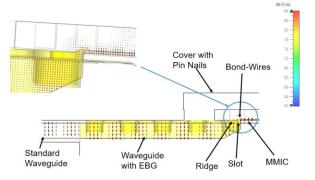
In this paper, a novel transition for chip-to-waveguide interconnection via direct gold wirebonding is proposed. In this approach, there is no need for any intermediate probe or transfer substrate between the chip and the GWG line. The proposed substrate-less transition working at D-band is illustrated in Figure 6. A GWG line is designed at the left side, and the other side is a GSG pad with microstrip line on GaAs substrate which is compatible with most of MMICs. In order to force the f ields to propagate into the GWG and suppress unwanted radiation at the transition, a simple periodical nail structure is applied and designed at the top of the transition. The inner two nails are shorter than other nails for leaving enough space for the bond - wires. Two gold bond-wires using JEDEC 4-point structure for a better impedance matching are used to connect the signal line of
MMIC to a ridge on GWG’s upper metal layer.
The geometry parameters of the design D-band transition are given in Table I. As can be seen in Figure 7 (a), the transition is a quasi-planar structure and the electromagnetic wave is guided into the GWG effectively.
11 |
www.videleaf.com |
Prime Archives in Sensors: 2nd Edition
Table 1: Optimum geometry parameters for MMIC to GWG based on glideholly EBG.
Parameter |
Value(mm) |
Parameter |
Value (mm) |
|
|
|
|
W1 |
0.373 |
Wm |
0.035 |
|
|
|
|
W2 |
0.1 |
tm |
0.05 |
|
|
|
|
L1 |
0.34 |
Wpin |
0.4 |
|
|
|
|
L2 |
0.15 |
Lpin |
0.4 |
|
|
|
|
Dw |
0.025 |
Hpin |
0.5 |
|
|
|
|
Hw |
0.03 |
Hpin1 |
0.4 |
|
|
|
|
D |
0.2 |
p |
0.8 |
|
|
|
|
Slot_W |
0.6 |
Slot L |
1.3 |
|
|
|
|
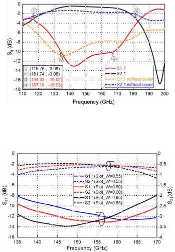
Figure 7 (a) shows the electric field distribution of the transition from the view of the middle cutting plane. It could be seen that the transmitted signal couples to the waveguide via the bond - wire. The unwanted radiation at the transition is minimized b y using the periodical pin structure. The frequency responses of the transition with and without periodical pin are shown in Figure7(b). Considering lossy aluminum of 3.56×10⁷ S/m for the GWG line, and lossless GaAs for MMIC, it is obtained a return loss above 10 dB within the 134-167 GHz band and a low insertion loss of 0.8 dB including all losses from chip to the waveguide port.
(a)
12 |
www.videleaf.com |
Prime Archives in Sensors: 2nd Edition
(b)
Figure 7: Substrate-less transition, (a) E-field distribution of the transition; (b) simulated performances of the transition.
Figure 8: Effect of the slot width (slot_W) on the designed transition frequency response.
13 |
www.videleaf.com |
Prime Archives in Sensors: 2nd Edition
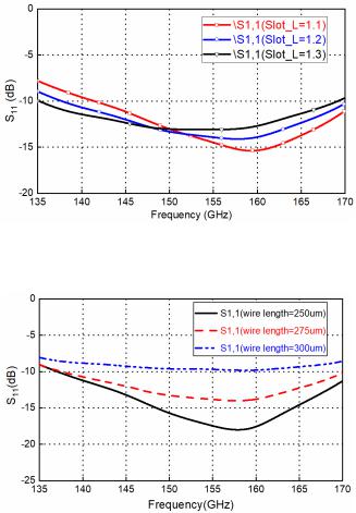
Figure 9: Effect of the slot length (slot_L) on the designed transition frequency response.
Figure 10: Effect of the bond-wire length on the designed transition frequency response.
Usually CNC milling Machine are used for the waveguide and leak proof cover. WEDM-LS are used to machining of highprecision deep hole with small diameter for the upper layer’s EBG hole. Some parameter studies for the proposed transition (focused on 135-170 GHz for acceptable return loss) are presented in this section. These parameter study could be used for the design and sensitivity analysis of the transition. Figure 8 shows the slot width (slot_W) effects on the frequency response of the transition. It can be seen the frequency response shifts
14 |
www.videleaf.com |
Prime Archives in Sensors: 2nd Edition
towards lower frequencies when increasing the width from 0 .55 mm to 0.65 mm. The transition loss is below 1 dB and shows insusceptibility with the slot width. Figure 9 shows the slot length (slot_L) effects on the frequency response of the transition. It can be seen the frequency response shifts towards lower frequencies when increasing the length f rom 1 .1 mm to 1.3 mm, while 10 dB return loss bandwidth remains basically unchanged. Using high-precision wedge-wedge wire bonder, the minimum value of wire arc height Hw is 20 μm. Under ultra-low Hw condition, the distance between two bonding pad D could be less than 150 μm. Thus the minimum wire bond-wire length is about 187.5 μm. Considering small deviation for bonding point, the bond-wire length will be changed. Figure 10 depicts the bond-wire length effects on the transition. When the length changes from 250 μm to 300 μm, great sensitivity with this parameter is observed. A shorter bond-wire would provide better return loss and better insertion loss. Precise dimensional control must be done with this parameter during the assembly.
Table 2: Optimum Dimension Parameters for MMIC to Waveguide transition based on glide-holly EBG at E band.
Parameter |
Value(mm) |
Parameter |
Value (mm) |
W1 |
0.5 |
Wm |
0.035 |
W2 |
0.18 |
tm |
0.05 |
L1 |
0.565 |
Wpin |
0.5 |
L2 |
0.15 |
Lpin |
0.5 |
Dw |
0.025 |
Hpin |
0.9 |
Hw |
0.03 |
Hpin1 |
0.8 |
D |
0.35 |
p |
1 |
Slot_W |
1.1 |
Slot L |
2.9 |
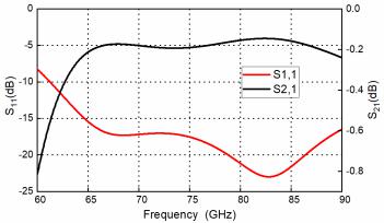
Considering the Mixer’s LO frequency of E-band, the transition with the same structure like D-band have been also investigated at E-band. The design parameters are shown in Table II, and the simulated results are shown as Figure11. The transition has an insertion loss better than 0.2 dB, and a return loss above 15 dB for almost the whole E band.
15 |
www.videleaf.com |
Prime Archives in Sensors: 2nd Edition
Figure 11: Simulated frequency response of the designed E-band transition.
Mixer Packaged Module Configuration and
Design
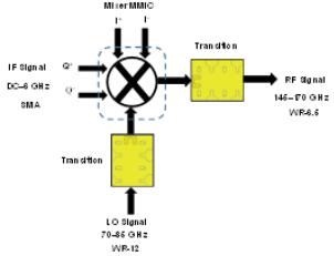
For the design of D-band mixer packaging module, we choose a subharmonic mixer chip, with part number GMDR0035A from Gotmic AB. Typical performance values for this mixer mmic are shown in Table 3. The chip is realized on GaAs substrate and operates in the 145-170 GHz band for RF with 70 -85 GHz f or LO, suitable for D-band point-to-point communication, sensing and imaging application. The basic block diagram of subharmonic mixer is shown as Figure 12. Figure 13 shows the bottom part of the design module, which houses the MMIC, the input/output waveguide channel, and PCB that provides dc and IQ lines to MMIC. LO/RF signals are transmitted in the EBG waveguides and connected with the mixer chip by wire-bonding directly. Differential I/Q IF signals (0-6 GHz)are provided with coaxial interfaces like SMA connectors. For on the PCB board, only differential I/Q signal and DC feed need to be traced, a lowcost substrate could be used. We have used the Rogers RO 4003C that provides a stable dielectric constant and low-loss tangent factor at RF band. The PCB substrate thickness is 0.508 mm and is gold plate afterward to be able to apply wire-bonding. At operating frequency, the dielectric constant of this substrate is 3.55, its loss tangent is 0.0027, and the 50Ω microstrip line
16 |
www.videleaf.com |
Prime Archives in Sensors: 2nd Edition
width is about 1 mm. The top part acts as a metal box with pin structures covering the LO and RF transitions.
Table 3: Typical performance values of chip GMDR0035A.
Parameter |
|
Min |
Typ |
Max |
Unit |
RF frequency |
|
140 |
|
170 |
GHz |
IF frequency |
|
DC |
|
6 |
GHz |
LO frequency |
|
70 |
|
85 |
GHz |
|
|
|
|
|
|
LO input power |
|
|
15 |
|
dBm |
LO multiplication |
factor |
|
2 |
|
|
Conversion loss |
|
|
12 |
|
dB |
P1dB |
|
|
-5 |
|
dBm |
RF return loss |
|
10 |
|
|
dB |
IF return loss |
|
10 |
|
|
dB |
LO return loss |
|
10 |
|
|
dB |
Figure 12: Block diagram of IQ subharmonic up-mixer.
17 |
www.videleaf.com |
Prime Archives in Sensors: 2nd Edition
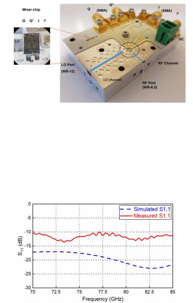
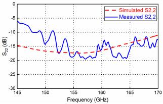
Figure 13: Fabricated D band Mixer assembly and detailed transition with the waveguide.Measurement has been performed to characterize the packaged mixer with Keysight PNA-X N5247A and a E-band frequency extender for LO port, while with Keysight PNA-X and D-band VDI frequency extender for RF port separately. The LO/RF ports measured return loss for the mixer is shown as Figure 14, and S11 is below -10 dB in most of the operating LO and RF working frequency band which is acceptable for D-band Mixer module. The simulated transition performance (ideal matching load port) and measured transition performances (real Mixer port) show apparent differences, which are mainly caused by the mismatch between transition and mixer chip
(GMDR0035A mixer presenting the port’s return loss of 10 dB).
(a)
18 |
www.videleaf.com |
Prime Archives in Sensors: 2nd Edition
(b)
Figure 14: Return loss vs frequency for LO signal port (a) and RF signal port
(b) matching load
The presented work is also compared with state-of -art packaging techniques reported in the literature in Table . The comparison shows the presented work exhibits the widest continuous working bandwidth with active MMIC, and one of the lowest insertion loss while at the same time providing a substrate-less packaging solution.
To measure the up-converter mode as a transmitter, mixer measurement mode of Keysight PNA-X N5247A and a D-band VDI frequency extender were used. IF signal with the quadrature differential input signal was generated by PNA-X through a quadrature coupler and two baluns. The LO signal is provided from an Agilent 8257D synthesizer together with a E -band x6 multiplier module. The measured conversion loss and output power of the mixer with up-converter mode as a transmitter is shown in Figure15 and Figure16. The typical gate bias voltage (Vg) for the Mixer is -1.4 V which ranging from -1.7 V to -1.1 V according to the GMDR0035A datasheet. Three bias points are chosen to examine the optimum working condition. IF is fixed at 2 GHz and LO is swept to cover RF at 145 -170 GHz upper side band). The fixed frequency response with swept IF power and several bias points is shown at Figure 17. With lower bias voltage, the mixer’s conversion loss will be better while output saturation comes earlier.
19 |
www.videleaf.com |
Prime Archives in Sensors: 2nd Edition
Table 4: Measurements Comparison of D-band Transition.
No. |
Process |
Measured Topology |
Bandwidt |
Freq |
Insertion |
Return |
|
|
|
h |
Band/GHza |
Loss/dBb |
Loss/dBc |
[6] |
SiGe BiCMOS with |
Transition Antenna |
16.95% |
135-160 |
4.2-5.5 |
>5 |
|
Heterogeneous Integration |
|
|
|
|
|
[36] |
SiC chip with |
Transition with ML |
23.7% |
125-137 |
0.7 |
~12 |
|
Nongalvanic packaging |
Back-to-Back |
|
147-170 |
|
|
[37] |
127 μm-thick quartz with |
Transition with ML |
16.4% |
144.7-170 |
2 |
10 |
|
Bonding-wire Interconnect |
Single-ended |
|
|
|
|
[38] |
eWLB with Silicon Taper |
Transition with ML |
26% |
116-151 |
3.4 |
5 |
|
Interconnect |
Single-ended |
|
|
|
|
This |
GaAs chip with |
Transition with Mixer |
21.92% |
134-167 |
0.8 |
>10 |
work |
Substrate-Less Packaging |
Single-ended |
|
|
|
|
a working frequency band with return loss better than 10 dB. b Average insertion loss.
c Maximum return loss.
20 |
www.videleaf.com |