

диафрагмированные волноводные фильтры / 2e5158a5-5cdd-4c32-9bde-0b6f5988ba74
.pdfIET Microwaves, Antennas & Propagation
Research Article
Design of a dual-band waveguide filter based on micromachining fabrication process
ISSN 1751-8725
Received on 30th July 2015 Revised on 14th November 2015 Accepted on 15th December 2015 doi: 10.1049/iet-map.2015.0489 www.ietdl.org
Xin Cao , Zongxi Tang, Jingfu Bao
School of Electronic Engineering, University of Electronic Science and Technology of China, No. 2006, Xiyuan Road, Hightech Area (west), Chengdu 611731, People’s Republic of China
E-mail: 798899759@qq.com
Abstract: In this study, a dual-band waveguide filter based on micromachining fabrication process in terahertz is proposed. The proposed filter employs a pair of four-stage rectangular waveguide resonators based on the parallel structure and the centre frequencies of the two passbands are designed at 240 and 300 GHz with the relative bandwidths of 4.2 and 3.3%. The isolation between the two passbands has been achieved over 40 dB. The simulated and measured results are in good agreement and the proposed filter can be applied in the millimetre wave communication systems.
1 |
Introduction |
|
|
|
|
|
|
|
|
|
|
|
|
The equivalent circuit based on the K-inverter is shown in Fig. 2. |
||||||||||||||||||||||||||||||||||||||||||
|
|
|
|
|
|
|
|
|
|
|
|
|
|
|
|
|
The normalised K can be defined as |
|
|
|
|
|
|
|
|
|
|
|
|
|
|
|
||||||||||||||||||||||||
The electromagnetic (EM) waves in terahertz (THz) have many |
|
|
|
|
|
|
|
|
|
|
|
|
|
|
|
|
|
|
|
|
|
|
|
|
|
|
|
|
|
|
|
|
|
|
|
|
|
|
|
|||||||||||||||||
advantages such as fast data rate transportation, great directivity, |
|
|
|
|
|
|
|
|
|
|
|
|
|
|
|
|
|
|
|
|
|
|
|
|
|
|
|
|
|
|
|
|
|
|||||||||||||||||||||||
become a |
hot |
research |
area all |
over the |
world during the years |
|
|
|
|
|
|
|
|
|
|
|
|
|
|
|
|
|
|
|
|
|
|
|
|
|
|
|
|
|
|
|
|
|||||||||||||||||||
high |
reliability |
and low |
power |
dissipation. THz technology |
has |
|
|
|
|
|
|
|
|
|
|
|
|
|
|
K = |
|
|
|
|
Z0 |
|
|
|
|
|
|
|
|
|
|
|
(3) |
|||||||||||||||||||
|
|
|
|
|
|
|
|
|
|
|
|
|
|
|
|
|
Zin |
|
|
|
|
|
|
|
|
|
|
|
||||||||||||||||||||||||||||
[1, 2]. Waveguides are widely used in filters, power dividers and |
|
|
|
|
|
|
|
|
|
|
|
|
|
|
|
|
|
|
|
|
|
|
|
|
|
|
|
|
|
|
|
|
|
|
|
|
|
|
|
|||||||||||||||||
directional couplers for their high quality factor and low radiation |
|
|
|
|
|
|
|
|
|
|
|
|
|
|
|
|
|
|
|
|
|
|
|
|
|
|
|
|
|
|
|
|
|
|
|
|
|
|
|
|||||||||||||||||
loss. Therefore, filters based on waveguides have the advantages |
Then the S-parameter of the network can be calculated as |
|
||||||||||||||||||||||||||||||||||||||||||||||||||||||
of low in-band insertion loss and excellent power capacity [3–6]. |
|
|
|
|
|
|
|
|
|
|
|
|
|
|
|
|
|
|
|
|
|
|
|
|
|
|
|
|
|
|
|
|
|
|
|
|
|
|
|
|||||||||||||||||
Filters working at THz are much smaller than those working at |
|
|
|
|
|
|
|
|
|
|
|
1 |
|
|
K2 |
j |
|
|
|
2K |
|
|
|
|
||||||||||||||||||||||||||||||||
gigahertz |
(GHz) |
or |
megahertz. |
Micromachining |
based |
on |
|
|
|
|
|
|
|
|
|
|
|
|
|
|
|
|
|
|
|
|
|
|
|
|
|
|
|
|
|
|
|
|
|
|
||||||||||||||||
|
|
|
|
|
|
|
|
|
|
1 |
+ |
|
|
|
|
|
|
|
|
|
1 |
+ |
2 |
|
|
|
|
|||||||||||||||||||||||||||||
lithography, inductively coupled plasma (ICP) etching and |
|
|
|
|
S |
|
|
|
|
|
|
|
|
|
|
|
|
|
|
|
|
|
(4) |
|||||||||||||||||||||||||||||||||
|
|
|
|
= |
− K2 |
|
|
|
|
|
|
K2 |
|
|
||||||||||||||||||||||||||||||||||||||||||
electroplating can achieve the precision up to micrometre (μm) |
|
|
|
|
|
|
|
j |
|
2K |
|
2 |
|
|
|
|
1 − K2 |
|
|
|
|
|||||||||||||||||||||||||||||||||||
|
|
|
|
|
|
|
|
|
|
|
|
|
|
|
|
|
|
|
|
|
|
|
|
|
|
|
|
|
|
|
|
|
|
|
|
|||||||||||||||||||||
scale, which is one of the development trends in THz fabrication |
|
|
|
|
|
|
|
|
|
|
1 |
+ |
K |
|
|
|
|
|
1 |
+ |
|
K |
|
|
|
|||||||||||||||||||||||||||||||
technology. In literatures [7–22], shielding wires, waveguides, |
Therefore |
|
|
|
|
|
|
|
|
|
|
|
|
|
|
|
|
|
|
|
|
|
|
|
|
|
|
|
|
|
|
|
|
|||||||||||||||||||||||
antennas, planar transmission lines and cantilever beams based on |
|
|
|
|
|
|
|
|
|
|
|
|
|
|
|
|
|
|
|
|
|
|
|
|
|
|
|
|
|
|
|
|
|
|
|
|
|
|
||||||||||||||||||
this fabrication process have realised excellent performance. |
|
|
|
|
|
|
|
|
|
|
|
|
|
|
|
|
|
|
|
|
|
|
|
|
|
|
|
|
|
|
|
|
|
|
|
2 |
|
|
|
|||||||||||||||||
In this paper, based on this micromachining fabrication process, a |
|
|
|
|
|
|
|
− |
|
|
|
|
|
|
|
|
|
|
|
|
|
|
|
|
|
|
|
|
|
|
|
|
|
|
|
|||||||||||||||||||||
|
|
|
|
|
|
|
|
|
|
|
|
|
|
|
|
|
|
|
|
|
|
|
|
|
|
|
|
|
|
|
|
|
|
|
|
|
|
|
|
|
|
|
||||||||||||||
|
|
|
|
|
|
|
|
|
|
|
|
|
|
|
|
|
|
|
|
|
|
|
|
|
|
|
|
|
|
|
|
|
|
|
|
|
|
|
|
|||||||||||||||||
|
|
|
|
|
|
|
|
|
|
|
|
|
|
|
|
|
|
|
|
|
|
1 |
|
|
|
|
|
|
|
|
|
|
|
|
|
|
|
|
|
|
|
|
|
|
|
|
|
|
|
|
||||||
dual-band waveguide filter is designed. The designed filter employs |
K |
= |
|
|
|
|
S11 |
|
= |
|
|
1 |
|
|
|
− |
|
|
|
1 |
|
− |
1 |
(5) |
||||||||||||||||||||||||||||||||
|
|
|
|
|
|
|
|
|
|
|
fi |
|
|
|
|
|
|
|
1 |
|
|
|
|
|
|
|
|
|
|
|
|
|
|
|
|
|
||||||||||||||||||||
the parallel structure and achieves two independent passbands. Also, |
|
|
+ |
S11 |
|
|
S21 |
|
|
|
S21 |
|
|
|||||||||||||||||||||||||||||||||||||||||||
the thickness and roughness of the metal layers are also taken into |
|
|
|
|
|
|
|
|
|
|
|
|
|
|
|
|
|
|
|
|
|
|
|
|
|
|
||||||||||||||||||||||||||||||
consideration during simulation. The |
lter is measured using vector |
|
|
|
|
|
|
|
|
|
|
|
|
|
|
|
|
|
|
|
|
|
|
|
|
|
and S11 |
of the |
||||||||||||||||||||||||||||
network analyser |
with |
frequency |
expansion networks and |
the |
From (5), K can be calculated based on the S21 |
|||||||||||||||||||||||||||||||||||||||||||||||||||
network. |
|
|
|
|
|
|
|
|
|
|
|
|
|
|
|
|
|
|
|
|
|
|
|
|
|
|
|
|
|
|
|
|
|
|
|
|
|
|
||||||||||||||||||
measured results are in satisfactory agreement with the simulated ones. |
|
|
|
|
|
|
|
|
|
|
|
|
|
|
|
|
|
|
|
|
|
|
|
|
|
|
|
|
|
|
|
|
|
|
|
|
|
|
||||||||||||||||||
The next step is to determine the phase shift arg(S21), which is |
||||||||||||||||||||||||||||||||||||||||||||||||||||||||
|
|
|
|
|
|
|
|
|
|
|
|
|
|
|
|
|
||||||||||||||||||||||||||||||||||||||||
|
|
|
|
|
|
|
|
|
|
|
|
|
|
|
|
|
caused by the phase delays of the irises θ0 and the metallic |
|||||||||||||||||||||||||||||||||||||||
2 Theory and design process |
|
|
|
|
|
waveguide θj. Since the irises can be seen as an inductor, then |
||||||||||||||||||||||||||||||||||||||||||||||||||
|
|
|
|
|
|
|
|
|
|
|
|
|
|
|
|
|
|
|
|
|
|
|
|
|
|
|
|
|
|
|
|
|
|
|
|
|
|
|
|
|
|
|
|
|||||||||||||
As shown in Fig. 1a, two rectangular resonant cavities are coupled |
|
|
|
|
|
|
|
|
|
|
|
|
|
|
|
u0 = 90◦ |
|
|
|
|
|
|
|
|
|
|
|
(6) |
||||||||||||||||||||||||||||
together using a pair of E-plane irises. This structure can be |
Then arg(S21) can be given as |
|
|
|
|
|
|
|
|
|
|
|
|
|
|
|
|
|
|
|
|
|
|
|
||||||||||||||||||||||||||||||||
modelled as a T-network comprised of series reactance XAj−1,j and |
|
|
|
|
|
|
|
|
|
|
|
|
|
|
|
|
|
|
|
|
|
|
|
|||||||||||||||||||||||||||||||||
parallel reactance |
XBj−1,j |
(shown |
in Fig. |
1b), and |
they can |
be |
|
|
|
|
1 |
|
|
|
|
|
|
|
|
|
|
|
|
|
|
|
|
|
|
|
|
|
|
1 |
|
|
|
|
|
|
|
|
||||||||||||||
calculated as [23] |
|
|
|
|
|
|
|
|
|
|
|
|
|
arg (S21) = |
uj−1 |
+ uj + u0 = |
uj−1 + uj + 90◦ |
(7) |
||||||||||||||||||||||||||||||||||||||
|
|
|
|
|
|
|
|
|
|
|
|
|
|
|
|
|
||||||||||||||||||||||||||||||||||||||||
|
|
|
|
|
|
|
|
|
|
|
|
|
|
|
|
|
2 |
2 |
||||||||||||||||||||||||||||||||||||||
|
|
|
|
|
|
|
|
|
1 |
|
S21 |
S11 |
|
|
|
|
|
|
|
|
|
|
|
|
|
|
|
|
|
|
|
|
|
|
|
|
|
|
|
|
|
|
|
|
|
|
|
|
|
|
|
|
|
|||
|
|
|
|
XAj−1,j |
= Z0 |
1 |
− + |
|
|
|
(1) |
To realise half-wavelength resonance, each segment of the |
||||||||||||||||||||||||||||||||||||||||||||
|
|
|
|
S11 S21 |
|
|||||||||||||||||||||||||||||||||||||||||||||||||||
|
|
|
|
|
|
|
|
|
|
− |
+ |
|
|
|
|
|
waveguide should be added an amended length len, which can be |
|||||||||||||||||||||||||||||||||||||||
|
|
|
XBj−1,j = Z0 |
|
|
|
|
2S21 |
|
|
|
|
(2) |
decided by the following equation |
|
|
|
|
|
|
|
|
|
|
|
|
|
|
|
|||||||||||||||||||||||||||
|
|
|
1 − 2S11 + S112 − S212 |
|
|
|
len |
|
|
|
1 |
|
|
|
|
|
|
|
|
|
|
|
|
|
|
|
|
|
|
|
|
|
|
|
|
|
|
|
|
|
||||||||||||||||
|
360◦ |
|
|
− |
|
|
arg |
|
S21 |
j−1 |
+ arg |
|
S21 j = 90◦ |
(8) |
||||||||||||||||||||||||||||||||||||||||||
As for E-plane irises, XBj−1,j > 0, therefore, this component can be |
lg |
2 |
|
|
||||||||||||||||||||||||||||||||||||||||||||||||||||
seen as an inductor, and the type of this coupling structure is |
|
|
|
|
|
|
|
|
|
|
|
|
|
|
|
|
|
|
|
|
|
|
|
|
|
|
|
|
|
|
|
|
|
|
|
|||||||||||||||||||||
parallel inductance coupling. |
|
|
|
|
|
|
|
|
where lg is the guided wavelength at the frequency f0, and it can be |
|||||||||||||||||||||||||||||||||||||||||||||||
IET Microw. Antennas Propag., 2016, Vol. 10, Iss. 4, pp. 459–463 |
|
|
|
|
|
|
|
|
|
|
|
|
|
|
|
|
|
|
|
|
|
|
|
|
|
|
|
|
|
|
|
|
|
|
|
|
|
|
|
|||||||||||||||||
& The Institution of Engineering and Technology 2016 |
|
|
|
|
|
|
|
|
|
|
|
|
|
|
|
|
|
|
|
|
|
|
|
|
|
|
|
|
|
|
|
|
|
|
|
|
|
|
|
459 |
||||||||||||||||
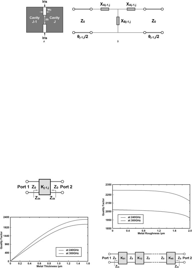
Fig. 1 Two coupled resonant cavities
a Physical structure b Equivalent circuit
calculated as
lg |
= |
|
|
|
1 |
|
|
f0/c |
2 |
− 1/2a |
2 |
||
|
|
|
||||
|
|
|
|
|
|
|
convenience of simulation process, the width of the irises w0 is fixed at 50 μm.
For n = 4, the element values for Chebyshev low-pass filter
(9)prototypes (0.01 dB ripple) are g1 = 0.7128, g2 = 1.2003, g3 =
1.3212, g4 = 0.6476, g5 = 1.1007. Based on the K-inverter transformation, it can be calculated that
The first step is to simulate the unloaded quality factor with different metal thickness and roughness. The metal type is set as Au with its corresponding conductivity of 4.1 × 10⁷ S/m. The EM simulation software used is HFSS and the solution type is set to be eigenmode. The quality factor is calculated based on the TE101 resonant mode of the rectangular metallic cavity. As shown in Fig. 3, with the increase of the metal thickness, the skin effect becomes less dominant. Above 1.4 μm, the quality factor is almost not affected by the thickness and the target Au thickness in the fabrication process is about 3 μm. As shown in Fig. 4, the quality factor drops dramatically after 1.6 μm, this is because surface roughness can increase the resistance of the metal layer, and high resistance causes more conductor loss, which eventually lowers the quality factor. Based on the fabrication process data provided by the manufacturer, the roughness can be controlled below 0.8 μm. Hence, from the analysis above, the fabricated Au layer can satisfy the quality factor requirements based on simulation.
The next step is to determine the coupling coefficients and the phase shift of the irises. In our design, four resonators are employed and coupled together for each one passband, as shown in Fig. 5. The standard waveguide WR-3 with the width of 0.8636 mm and height 0.4318 mm is chosen, and for the
K01 = K45 = 0.439, K12 = K34 = 0.149, K23 = 0.109 (10)
Let m be the gap width between two irises, and the coupling coefficient and the phase shift are simulated from m = 200–550 μm at 240 GHz. The simulated results are shown in Fig. 6. To satisfy (10), three points m1 = 535 μm, m2 = 390 μm and m3 = 360 μm can be found, then their corresponding phase shifts are arg(S21)1 = −148.6°, arg(S21)2 = −115.0° and arg(S21)3 = −148.6°. Based on (9), at 240 GHz, lg = 1.810 mm, and then from (8), the two amended
lengths can be calculated as len1 = 0.571 mm and len2 = 0.665 mm. Then, the simulated S-parameters of the first passband are shown in
Fig. 7. In this figure, it is shown that S11 is below 15 dB, therefore the results need further optimisation.
The design of the second passband is quite similar to the design of the first one. The K-inverters can be calculated as
K01′ = K45′ = 0.333, K12′ = K34′ = 0.085, K23′ = 0.063 (11)
The coupling coefficient and the phase shift are simulated from m = 200–450 μm at 300 GHz. The simulated results are shown in Fig. 8. Also in order to satisfy (11), three points m1′ = 430 μm, m2′ = 290 μm and m3′ = 360 μm can be found, then their corresponding
Fig. 2 Equivalent network based on the K-inverter
Fig. 4 Simulated quality factor with different metal roughness
Fig. 3 Simulated quality factor with different metal thickness |
Fig. 5 Equivalent circuit of one passband based on the K-inverter |
|
IET Microw. Antennas Propag., 2016, Vol. 10, Iss. 4, pp. 459–463 |
460 |
& The Institution of Engineering and Technology 2016 |
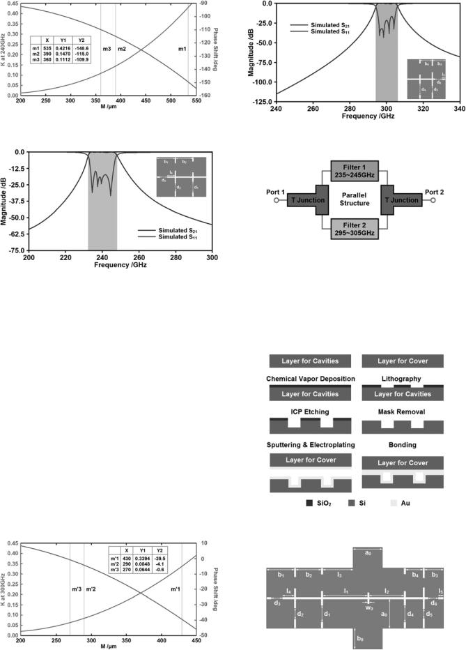
Fig. 6 Simulated K and arg(S21) with m from 200 to 550 μm
Fig. 9 Simulated S-parameters of the second passband
Fig. 10 Structure of the proposed filter
Fig. 7 Simulated S-parameters of the first passband
phase shifts are arg(S21)11′ = −39.5°, arg(S21)′2 = −4.1° and arg(S21)′3 = −0.6°. Based on (9), at 300 GHz, l′g = 1.225 mm, and then from
(8), the two amended lengths can be calculated as l′en1 = 0.213 mm
and l′en2 = 0.152 mm. Then, the simulated S-parameters of the second passband are shown in Fig. 9. Still, these results need
further optimisation.
The final step is to connect these two separate filters with input and output T-junctions based on the parallel structure to build up two passbands, as shown in Fig. 10. The advantage of this parallel structure is that each branch of the filter can be optimised separately, without major influence on the other branch. The final step in the design process is tuning and optimisation using EM simulation software HFSS. After satisfactory simulated results are obtained, the fabrication process then can be started.
3 Fabrication and measurement
The fabrication process is based on micromachining in micro-electromechanical systems (MEMS) technology (shown in Fig. 11). Two pieces of Si layers are prepared for fabrication. One is for cavities and the other is for the cover. First, a thin layer SiO2 is deposited on the Si layer using chemical vapour
deposition. The next step is lithography, etching the SiO2 to the desired pattern with no influence on the Si layer. Then, ICP etching is applied. The parts of the Si layer that are exposed to air are etched to the thickness of 0.4318 mm (the height of the standard waveguide WR-3), while the other parts of the Si layer are protected by SiO2 from etching. After the ICP etching process,
Fig. 11 Micromachining fabrication process
Fig. 8 Simulated K and arg(S21) with m from 200 to 450 μm |
Fig. 12 Topology of the proposed filter |
IET Microw. Antennas Propag., 2016, Vol. 10, Iss. 4, pp. 459–463 |
|
& The Institution of Engineering and Technology 2016 |
461 |
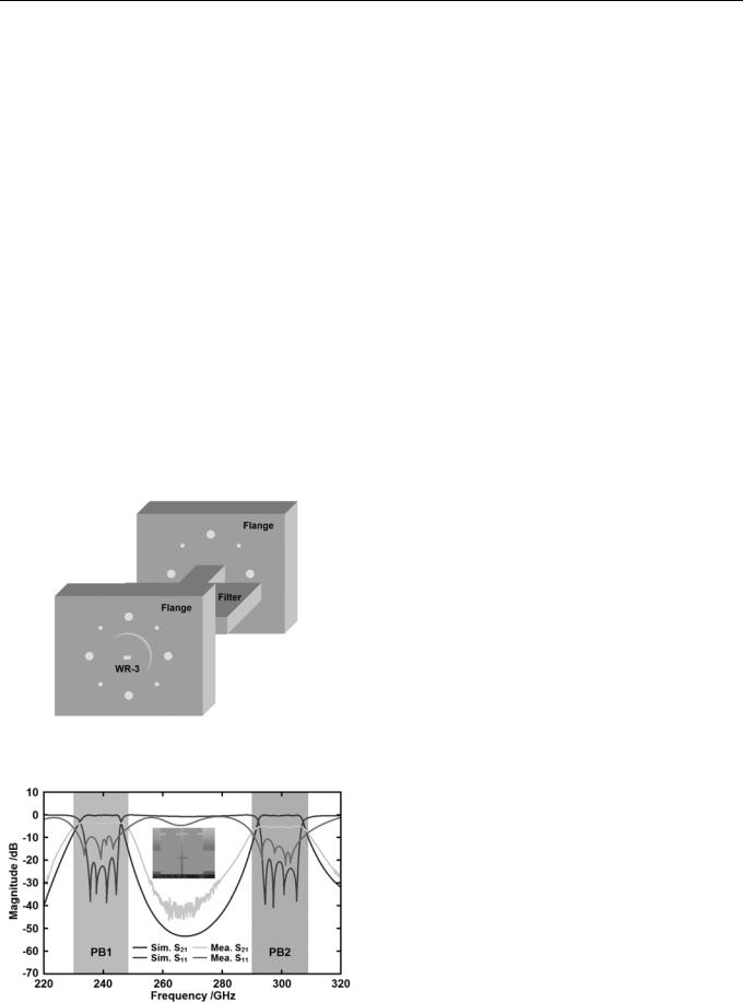
Table 1 Geometric parameters of the proposed filter (in mm)
Parameter |
Value |
Parameter |
Value |
Parameter |
Value |
Parameter |
Value |
|
|
|
|
|
|
|
|
w0 |
0.050 |
a0 |
0.864 |
b0 |
1.133 |
l1 |
1.320 |
l2 |
0.779 |
l3 |
0.893 |
l4 |
0.345 |
l5 |
0.155 |
b1 |
0.820 |
b2 |
0.744 |
b3 |
0.560 |
b4 |
0.507 |
d1 |
0.493 |
d2 |
0.339 |
d3 |
0.335 |
d4 |
0.506 |
d5 |
0.284 |
d6 |
0.301 |
|
|
|
|
the SiO2 is removed from Si. Then after mask removal, a thin layer of Au is sputtered and electroplated on the surfaces of the etched Si layer and the cover layer. The target thickness of the Au layer is about 3 μm. The final step is bonding these two layers to form the metallic waveguide.
The topology of the proposed filter is shown in Fig. 12 and the geometric parameters are listed in Table 1. The final simulated, measured results and the photograph of the fabricated filter under microscope are shown in Fig. 13. In the simulation process, Au boundary condition with the thickness of 3 μm and the roughness of 0.8 μm has been used. The simulated insertion losses of the first and the second passbands are 0.745 and 0.960 dB, respectively. The filter is measured in a fixture using vector network analyser with a pair of frequency expansion devices. The input and output ports of the fabricated filter are connected to the WR-3 waveguides using a pair of flanges, as shown in Fig. 14. The insertion loss of the first passband is about 3 dB with the relative
3 dB bandwidth of 4.2%, and the |
in-band return loss is over |
10 dB. As for the second passband, |
the insertion loss is around |
5 dB with the relative 3 dB bandwidth of 3.3%, and the return loss is also over 10 dB. The insertion loss is caused by the EM wave leakage due to the imperfect contact between the cover and the cavities, and by the roughness of the ICP etching process. The
measurement fixture can also bring about additional insertion loss. The isolation between the two passbands is about 40 dB. In general, the simulated and measured results are in good agreement.
4 Conclusion
In this paper, a dual-band waveguide filter based on micromachining fabrication process in THz is simulated, fabricated and measured. The proposed filter is based on the parallel structure with a pair of four-stage rectangular waveguide resonators. The measured results agree well with the simulated ones and good performance has been achieved, and the proposed filter can be applied in modern millimetre wave communication systems.
5 Acknowledgment
This work was supported by the National Natural Science Foundation of China (grant no. U1430102).
Fig. 13 Final simulated and measured results
Fig. 14 Structure of the test fixture
462
6References
1Nagatsuma, T.: ‘Terahertz technologies: present and future’, IEICE Electron. Express, 2011, 8, (14), pp. 1127–1142
2Fitch, M.J., Osiander, R.: ‘Terahertz waves for communications and sensing’, John Hopkins APL Tech. Dig., 2004, 25, (4), pp. 348–355
3Meng, H., Wu, K.L.: ‘Direct optimal synthesis of a microwave bandpass filter with
general loading effect’, IEEE Trans. Microw. Theory Tech., 2013, 61, (7), pp. 2566–2573
4Zhao, X.H., Bao, J.F., Shan, G.C., et al.: ‘D-band micromachined silicon rectangular waveguide filter’, IEEE Microw. Wirel. Compon. Lett., 2012, 22, (5), pp. 230–232
5Shi, Y.M., Barnet, L.R., Gamzina, D., et al.: ‘Terahertz vacuum electronic circuits fabricated by UV lithography molding and deep reactive ion etching’, Appl. Phys. Lett., 2009, 95, (18), p. 181505
6Leong, K.M.K.H., Henning, K., Zhang, C., et al.: ‘WR1.5 silicon micromachined waveguide components and active circuit integration methodology’, IEEE Trans. Microw. Theory Tech., 2012, 60, (4), pp. 998–1005
7Baghchehsaraei, Z., Vorobyov, A., Aberg, J., et al.: ‘Waveguide-integrated MEMS-based phase shifter for phased array antenna’, IET Microw. Antennas Propag., 2014, 8, (4), pp. 235–243
8Karim, M.F., Liu, A.Q., Ong, L.C., et al.: ‘Micromachined based narrow band Fabry–Perot tunable bandpass filter’, IET Microw. Antennas Propag., 2012, 6, (5), pp. 562–568
9Han, Z.L., Kohno, K., Fujita, H., et al.: ‘Tunable terahertz filter and modulator based on electrostatic MEMS reconfigurable SRR array’, IEEE J. Sel. Top. Quantum Electron., 2015, 21, (4), p. 2700809
10Angira, M., Rangra, K.: ‘Performance improvement of RF-MEMS capacitive
switch via asymmetric structure design’, Microsyst. Technol., 2015, 21, (7), pp. 1447–1452
11Xue, L., Wang, L., Xiong, T., et al.: ‘Analysis of dynamic performance of a Kalman filter for combining multiple MEMS gyroscopes’, Micromachines, 2014, 5, (4), pp. 1034–1050
12Lubecke, V.M., Mizuno, K., Rebeiz, G.M.: ‘Micromachining for terahertz applications’, IEEE Trans. Microw. Theory Tech., 1998, 46, (11), pp. 1821–1831
13Hyun, D., Yang, H.S., Park, H.S., et al.: ‘Dead-reckoning sensor system and
tracking algorithm for 3-D pipeline mapping’, Mechatronics, 2010, 20, (2), pp. 213–223
14Zhou, X.Y., Zhang, Z.Y., Fan, D.P.: ‘Improved angular velocity estimation using MEMS sensors with applications in miniature inertially stabilized platforms’, Chin. J. Aeronaut., 2011, 24, (5), pp. 648–656
15Liu, Y.M., Xu, J., Zhong, S.L., et al.: ‘Large size MEMS scanning mirror with vertical comb drive for tunable optical filter’, Opt. Lasers Eng., 2013, 51, (1), pp. 54–60
16Zhou, M., Meng, X., Qin, J.: ‘Building an EDM process model by an instrumental variable approach based on two interactive Kalman filters’, Precis. Eng., 2013, 37, (1), pp. 146–158
IET Microw. Antennas Propag., 2016, Vol. 10, Iss. 4, pp. 459–463 & The Institution of Engineering and Technology 2016
17Yan, J.Z., Seshia, A.A., Phan, K.L.: ‘Internal electrical and mechanical phase inversion for coupled resonator-array MEMS filters’, Sens. Actuators A, Phys., 2010, 158, (1), pp. 18–29
18Holzwarth, C.W., Khilo, A., Dahlem, M., et al.: ‘Device architecture and
precision |
nanofabrication |
of |
microring-resonator |
filter |
banks |
for |
integrated photonic systems’, |
J. |
Nanosci. Nanotechnol., 2010, 10, |
(3), |
|||
pp. 2044–2052 |
|
|
|
|
|
|
19Liu, Y., Zhao, D., Zhang, Y., et al.: ‘Research of autonomous navigation path planning based on the Sage_Husa adaptive filter for mobile robot’, Appl. Mech. Mater., 2013, 433–435, pp. 1567–1571
IET Microw. Antennas Propag., 2016, Vol. 10, Iss. 4, pp. 459–463 & The Institution of Engineering and Technology 2016
20Zuo, C., Sinha, N., Piazza, G.: ‘Very high frequency channel-select MEMS filters based on self-coupled piezoelectric ALN contour-mode resonators’, Sens. Actuators A, Phys., 2010, 160, (1-2), pp. 132–140
21Giner, J., Uranga, A., Torres, F., et al.: ‘Fully CMOS integrated bandpass filter based on mechanical coupling of two RF MEMS resonators’, Electron. Lett., 2010, 46, (9), pp. 640–641
22Groppi, C.E., Love, B., Underhill, M., et al.: ‘Automated CNC micromachining for integrated THz waveguide circuits’. 21st Int. Symp. on Space Terahertz Technology, Oxford, UK, March 2010, pp. 291–294
23Pozar, D.M.: ‘Microwave engineering’ (Wiley, 2011, 4th edn.)
463