

диафрагмированные волноводные фильтры / f2ca998f-84c3-4e01-89fa-fb28c258050f
.pdfIEEE TRANSACTIONS ON MICROWAVE THEORY AND TECHNIQUES, VOL. 47, NO. 12, DECEMBER 1999 |
2325 |
Millimeter-Wave Ka-Band  -Plane
Diplexers and Multiplexers |
|
Yu Rong, Senior Member, IEEE, Hui-wen Yao, Senior Member, IEEE, Kawthar A. Zaki, Fellow, IEEE, and Tim G. Dolan |
|
AbstractÐMillimeter-wave H-plane diplexers/multiplexers are |
|
designed using modified H-plane waveguide T-junctions and |
|
modified inductive window bandpass filters. Modeling of the |
|
diplexers/multiplexers are performed using the full-wave mode- |
|
matching method to obtain the generalized scattering matrices of |
|
the building blocks and by the cascading procedure to provide the |
|
overall frequency response. A complete systematic optimization |
|
procedure leads to the desired diplexer/multiplexer design. The |
(a) |
validity of employing the modified H-plane T-junctions in the |
|
diplexer/multiplexer configurations are demonstrated by the design examples. A millimeter-wave Ka upper band diplexer based on the simulated results was built and tested. Without any tuning, excellent experimental results are obtained, which verified the full-wave mode-matching-based precise design.
I. INTRODUCTION
THE increasing development of millimeter-wave technology greatly stimulates the need for compact lowloss millimeter-wave diplexing or multiplexing components,
which serve as channel separators.  -plane T-junction connected diplexers/multiplexers, shown in Fig. 1, are commonly used [1], [2], where the channel filters are either inductivewindow or metal-insert bandpass filters. In the literature, the diplexer/multiplexer design is usually performed by following one of two methods. For each of these two methods, the channel filters are usually designed first to achieve the required channel performances before they are plugged into the diplexer/multiplexer configurations. In the first method [1], the channel filters are re-optimized within the diplexer/multiplexer environment, which includes the T-junction discontinuity effect as well as the interaction between the channel filters. For the second method [2], the original channel filter designs are maintained and additional matching elements are incorporated into the channel paths to obtain an acceptable return loss of the diplexer/multiplexer unit.
The standard  -plane T-junction, shown in Fig. 2(a), has poor characteristics in the upper band that present problems in the diplexer/multiplexer design. The conventional design is not successful for upper band frequency if the above-mentioned first method is used [2]. On the other hand, the overall dimension of the designed diplexer/multiplexer using the second
Manuscript received March 26, 1999; revised July 15, 1999.
Y. Rong was with the Department of Electrical Engineering, University of Maryland at College Park, College Park, MD 20742 USA. He is now with Paratek Microwave Inc., Columbia, MD 21045 USA.
H. Yao is with Orbital Sciences Inc., Germantown, MD 20874 USA.
K. A. Zaki is with the Department of Electrical Engineering, University of Maryland at College Park, College Park, MD 20742 USA.
T. G. Dolan is with K&L Microwave Inc., Salisbury, MD 21801 USA. Publisher Item Identifier S 0018-9480(99)08427-6.
(b)
(c) |
|
Fig. 1. Configurations of the millimeter-wave |
H-plane diplexers/ |
multiplexers. |
|
method is too long due to the matching elements, especially for wide-band applications. Recent contributions [3], [4] may be applied to the design of the  -plane diplexers/multiplexers, however, the resultant structures are cumbersome and cannot meet the system compactness requirement for certain applications. The round corners in the
  -plane, resulting from the manufacturing process in the inductive windows channel filters, as shown in Fig. 2(b), are unavoidable due to the finite tool radius. This problem is not serious for diplexers/multiplexers operating at lower frequency bands. As the operation frequency increases, especially to millimeterwave frequency, the dimension of the diplexer/multiplexer is small. The influence of these round corners on the performance of the diplexer/multiplexer becomes critical. Very small radius for these corners is required; otherwise the performance of
0018±9480/99$10.00 ã 1999 IEEE

2326 |
IEEE TRANSACTIONS ON MICROWAVE THEORY AND TECHNIQUES, VOL. 47, NO. 12, DECEMBER 1999 |
(a)
(b)
Fig. 2. (a) Standard H-plane T-junction. (b) Standard inductive window bandpass filters.
(a)
(b)
Fig. 3. (a) Modified H-plane T-junction. (b) Modified inductive window bandpass filters with round corners in the E-plane.
becoming possible. The inclusion of the  -plane round corners of the modified inductive window bandpass filters in the modeling allows the use of relatively large radius tools, and thus avoids the manufacturing difficulty for these corners.
A full-wave mode-matching method is employed in the analysis of the diplexer/multiplexers. By computing the generalized scattering matrices of all the discontinuities involved and cascading the generalized scattering matrices of all the building blocks, the performance of the diplexers/multiplexers can be obtained. In order to drastically reduce the computation time, special techniques [7] are applied. A systematic optimization approach leads to the desired multiplexer design. Design examples of optimized diplexers /multiplexers operating in the 
 upper band are given to demonstrate the validity of employing the modified
  -plane T-junction in the diplexer/multiplexer configurations. Based on the simulation, a
 upper band diplexer was manufactured and tested. Measurements showed excellent agreement with the theoretical results. Without any tuning, all the specifications are met and
20-dB return losses in both of the channels of the diplexer are obtained.
II. T-JUNCTION DESIGN CRITERIA
The basic building block of the configurations shown in Fig. 1 is a lossless reciprocal three-port network, whose two ports (ports 1 and 2) are connected by the two channel filters: Filters 1 and 2. Suppose that the lossless reciprocal three-port junction, i.e., generalized T-junction, is characterized by its dominant mode scattering matrix 


 . By following the same arguments used in [4], it can be easily shown that if the generalized T-junction has the following properties, channel filters of the desired building block will have maximum bandwidths:
1) |
, |
, and |
, where the |
|
prime indicates derivative with respect to |
; |
|
2) |
larger transmissions |
and |
and |
|
; |
|
|
3) reflections 


 .
.
The above conditions are the same as [4], where symmetrical T-junctions are considered.
III. MODELING
the diplexer/multiplexer will deteriorate. However, this often presents problems in practice, especially for the applications where production in quantity is needed.
To overcome the above-mentioned problems, the following strategies are proposed for the design. The standard  -plane T-junction, shown in Fig. 2(a), in the diplexer/multiplexer configurations is replaced by the modified T-junction, shown in Fig. 3(a), which is preferred to the structures described in [5] and [6] because it avoids complexities of manufacturing. The standard inductive window bandpass filters, shown in Fig. 2(b), are replaced by the modified inductive window bandpass filters, as shown in Fig. 3(b). The performance of the modified T-junction can be controlled by varying the dimension of the inserted metal slab. This leads to the design of the diplexers/multiplexers with wider band channel filters
The first step in modeling the diplexer/multiplexer is to model the key building blocks, i.e., the modified  -plane T-junction and modified inductive window channel filters, individually to find their generalized scattering matrices.
To model the modified  -plane T-junction, the three-plane mode-matching method [8] was employed. In this method, the side arm (port 3) of the T-junction is terminated by three different lengths of shorted waveguide. The resultant structures are three two-port waveguide networks. Each of the three twoport networks is a cascade of waveguide step discontinuities. The three-port scattering matrix of the T-junction can be extracted from the scattering matrices of the three two-port waveguide networks. Based on the T-junction design criteria given above, appropriate values of
  and
and  in Fig. 3(a) are obtained by simple optimization. Fig. 4 shows the computed

RONG et al.: MILLIMETER-WAVE -BAND -PLANE DIPLEXERS AND MULTIPLEXERS |
2327 |
(a)
(b)
Fig. 4. Performance comparison of: (a) the standard waveguide WR28 H-plane T-junction and (b) the modified waveguide WR28 H-plane T-junction, where w = 0:08 in, t = 0:14 in.
 -parameters of the standard and designed modified
  -plane T-junctions. Much better characteristics of the modified T- junction approximating the desired design criteria have been obtained.
To model the modified inductive window bandpass filter, the  -plane round-corner inductive windows, shown in Fig. 3(b), should be modeled first. To do that, the
  -plane round corners are discritized as a number of waveguide steps, as shown in Fig. 5. This discontinuity can then be regarded as a cascade of several waveguide steps connected by waveguide sections with different heights. Modeling of this discontinuity can be performed by using the cascading algorithm [9]. By following the same way, the generalized scattering matrices of the whole filter can be derived.
The final step of modeling the diplexers/multiplexers is to get the return losses at all ports and the transmissions from the common port to channel filters. To do that, matching
Fig. 5. Configuration of the waveguide step with E-plane round corners, where the round corners are discretized for analysis.
loads should be connected to the corresponding ports in the configurations. Since the three-port modified  -plane T-junction and the modified inductive window channel filters
2328 |
IEEE TRANSACTIONS ON MICROWAVE THEORY AND TECHNIQUES, VOL. 47, NO. 12, DECEMBER 1999 |
are characterized by their generalized  -parameters, the overall
  -parameters of the resultant networks can be obtained by cascading their network parameters, where terminal connection
conditions between networks can be applied.
IV. OPTIMUM DESIGN
The optimum design of the generalized diplexer/multiplexer is primarily based on the optimization. A carefully constructed objective function and a prudent strategy of the optimization are necessary. The objective function must be constructed in such a way that the error between the computed performance of the designed diplexer and the required specifications must be efficiently expressed. Assume that the required specifications for the  th channel input reflection in the passband and transmissions in the transition/stopband are


 and
and 


 , respectively. The computed return loss and the transmission of the
  th channel are


 and
and 


 , respectively, where
  are a set of diplexer/multiplexer parameters. The following objective function can be defined in the meansquare sense:
where


 , the sets of the lower bounds and upper bounds of the optimization variables.
  and
and  are the sample points taken in the
  th passband and transition/stopband of the diplexer/multiplexer, respectively.
  equals zero if the computed values at the sampled frequencies satisfy the specification, otherwise one.


 and
and 


 are corresponding weighting factors.
  is the total number of the multiplexer channels (for diplexers,

 ).
).  is the total number of the sampled frequency points. Obviously, the design becomes a constrained nonlinear optimization problem.
The computer-aided design is carried out in a two-step optimization procedure by using an IMSL1 optimization program, where the quasi-Newton gradient algorithm is applied. To apply the optimization to the design of the diplexers/multiplexers, initial values of the diplexers/multiplexers must be provided. The initial dimensions of the channel filters can be obtained based on the individual filter designs satisfying the given specifications using the procedures in [9]. The initial lengths of the connecting waveguides in the manifold are chosen based on [2]. In the first step of the optimization, only the manifold parameters, i.e., lengths of the connecting waveguides, are optimized. In the second step of optimization, more diplexer parameters are needed to be included in the optimization. The resonators and inverters in the channel filters closer to the modified  -plane T-junctions in the manifold should be included earlier in the optimization. The obtained parameters
1 IMSL Math/Library User's Manual, version 1.0, IMSL, Houston, TX, 1987.
(a)
(b)
(c)
Fig. 6. The frequency responses (a)±(c) of H-plane diplexers of the configurations shown in Fig. 1(a)±(c), respectively. [First step optimization: reflection (dashed±dotted line), transmission (dotted line). Final optimization: reflection (solid line), transmission (dashed line)].
of the resonators and inverters after the present iteration are used as the initial values of the following iteration of the optimization. This step is repeated until all the required diplexer/multiplexer specifications are satisfied.
V. NUMERICAL RESULTS
To verify the validity of employing the modified  -plane T-junction in the multiplexer configurations, diplexer designs of the three configurations shown in Fig. 1 are performed first to achieve the following specifications:
Center frequencies |
37.8 GHz for Ch. 1; |
|
|
|
39.1 GHz for Ch. 2; |
Passband ripple |
|
less than 0.2 dB; |
0.2 dB bandwidth |
450 MHz excluding; |
|
Rejection at |
1.1 GHz |
larger than 65 dB; |
Insertion loss at |
|
less than 1.2 dB; |
VSWR at all ports in the passbands |
18 dB min. |
|
The first optimization step requires less than 1 min of execution time on a SUN ultra-10 work station. The second optimization step requires additional several minutes. The

RONG et al.: MILLIMETER-WAVE -BAND -PLANE DIPLEXERS AND MULTIPLEXERS |
2329 |
(a)
(a)
(b)
(b)
Fig. 7. Frequency response of the H-plane triplexer of the configurations shown in Figs. 1(b) and (c), respectively. [First step optimization: reflection (dashed±dotted line), transmission (dotted line), final optimization: reflection (solid line), transmission (dashed line)].
computed frequency responses of the diplexers are presented in Fig. 6. The optimized diplexers of the three configurations
have better than |
25-dB return loss in the |
passbands of |
the channels. All |
of the three configurations |
have 10-dB |
return loss in the passbands of the channels after the first optimization step. This indicates that good initial values of diplexer parameters are obtained through the process described above.
The triplexer designs is performed to demonstrate the validity of employing the modified  -plane T-junction in the upper band multiplexer design. The center frequency and bandwidth of the additional channel is 36.5 GHz and 450 MHz, respectively. The rejection and return-loss requirements maintain the same as those for the diplexer design. Following the fullwave mode-matching-based design procedures, the designs of two upper band
  -plane triplexers of the configurations, shown in Figs. 1(b) and (c), respectively, can also be readily
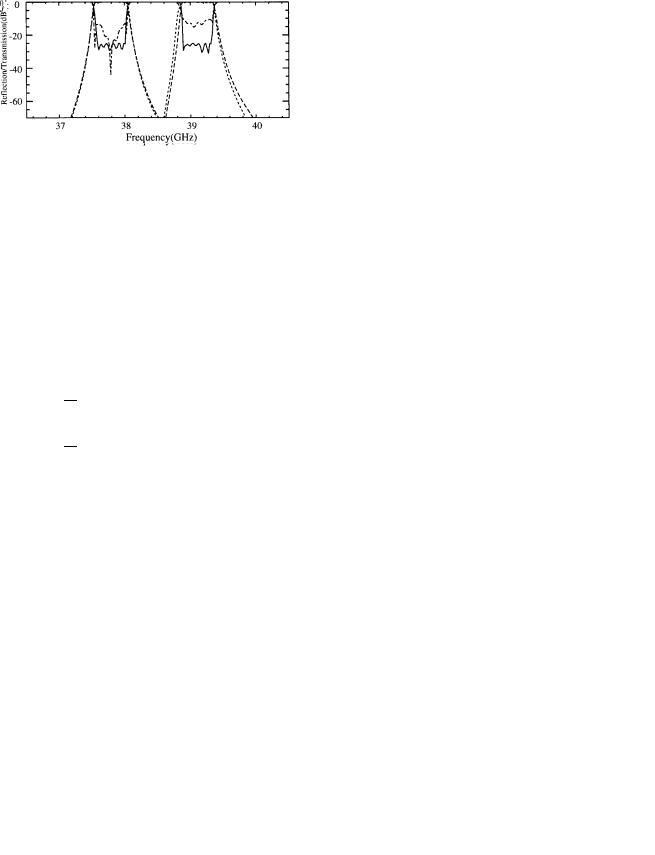
Fig. 8. (a) Simulated performance and (b) experimental performance of the no tuning H-plane diplexer of the configuration shown in Fig. 1(a).
obtained. Both of the triplexers have better than 25-dB return losses in the channels, as shown in Fig. 7. By performing the first optimization step, almost 10-dB return losses in the passbands of the triplexers are obtained.
To verify the accuracy of the design process, the above designed diplexer of the configuration, shown in Fig. 1(a), was built and tested. The measured results of the built diplexer is presented in Fig. 8. Excellent agreement between the theory and experiment is observed. All the required specifications are satisfied and 20-dB return losses in the passbands of the diplexer channels in this millimeter-wave upper band are obtained without any tuning.
VI. CONCLUSION
Millimeter-wave  -plane diplexers or multiplexers constructed by using modified
  -plane waveguide T-junctions and modified inductive window channel filters are described.
A full-wave mode-matching method is performed to model the diplexers/multiplexers, rigorously taking into account the curvature in the corners of the inductive window bandpass filters. An efficient design algorithm for diplexers/multiplexers

2330 |
IEEE TRANSACTIONS ON MICROWAVE THEORY AND TECHNIQUES, VOL. 47, NO. 12, DECEMBER 1999 |
are presented. Validation of employing the modified  -plane T-junction in the diplexer/multiplexer configurations is demonstrated by design examples. A millimeter wave
 upper band diplexer was simulated, built, and tested. Excellent experimental results of the designed diplexers are obtained without any tuning, which confirms the accuracy of the optimum design.
ACKNOWLEDGMENT
The authors thank Dr. Ali E. Atia, Orbital Sciences Corporation, Germantown, MD, for his kind review of this paper.
REFERENCES
[1]G. L. Matthaei, L. Young, and E. M. T. Jones, Microwave Filters, Impedance-Matching Networks, and Coupling Structures. New York: McGraw-Hill, 1964, chs. 13 and 16.
[2]J. Uher, J. Bornemann, and U. Rosenberg, Waveguide Components for Antenna Feed Systems: Theory and CAD. Norwood, MA: Artech House, 1993, ch. 3.
[3]A. Morini, T. Rozzi, and M. Mongiardo, ªEfficient CAD of wide-band contiguous channel multiplexers,º in IEEE MTT-S Int. Microwave Symp. Dig., 1996, pp. 1651±1654.
[4]A. Morini and T. Rozzi, ªConstraints to the optimum performance and bandwidth limitations of diplexer employing symmetric three-port junction,º IEEE Trans. Microwave Theory Tech., vol. 46, pp. 242±248, Feb. 1996.
[5]K. Ogusu, ªDielectric waveguide corner and power divider with a metallic reflector,º IEEE Trans. Microwave Theory Tech., vol. MTT-32, pp. 113±116, Jan. 1984.
[6]J. Hirokawa, K. Sakurai, M. Ando, and N. Goto, ªAn analysis of waveguide T-junction with an inductive post,º IEEE Trans. Microwave Theory Tech., vol. 39, pp. 563±566, Mar. 1991.
[7]J.-F. Liang and K. A. Zaki, ªCAD of microwave junctions by polynomial curve fitting,º in IEEE MTT-S Int. Microwave Symp. Dig., 1993, pp. 451±454.
[8]X.-P. Liang, K. A. Zaki, and A. E. Atia, ªA rigorous three plane mode-matching technique for characterizing waveguide T-junctions, and its application in multiplexer design,º IEEE Trans. Microwave Theory
Tech., vol. 29, pp. 2138±2147, Dec. 1991.
[9] H.-W. Yao, A. E. Abdelmonem, J.-F. Liang, X.-P. Liang, and K. A. Zaki, ªWide-band waveguide and ridge waveguide T-junctions for diplexer applications,º IEEE Trans. Microwave Theory Tech., vol. 41, pp. 2166±2173, Dec. 1993.
Yu Rong (S'97±SM'99), for photograph and biography, see this issue, p. 2324.
Hui-wen Yao (S'92±M'95±SM'97) received the B.S. and M.S. degrees from Beijing Institute of Technology, Beijing, China, in 1983 and 1986, respectively, and the Ph.D. degree from the University of Maryland at College Park, in 1995, all in electrical engineering.
From 1986 to 1991, he was a Lecturer in the Department of Electrical Engineering, Beijing Institute of Technology, where his research dealt mainly with electromagnetic (EM) radiation, scattering, and antenna design. From 1991 to 1992,
he was a Teaching Assistant in the Electrical Engineering Department, Wright State University, Dayton, OH, where he was involved with microstrip circuits and transient scattering by cylinders. From 1992 to 1995, he was a Research Assistant in the Department of Electrical Engineering, Microwave Laboratory, University of Maryland at College Park, where he was involved with the analysis, modeling, and design of microwave and millimeter-wave devices and circuits. From December 1995 to August 1997, he was with the Space System Group, CTA Inc., Rockville, MD. Since August 1997, he has been with Orbital Sciences Corporation, Germantown, MD, where he is involved with telecommunications and satellite communications.
Kawthar A. Zaki (SM'85-F'91), for photograph and biography, see this issue, p. 2324.
Tim G. Dolan received the B.S. degree in electrical engineering from Pennsylvania State University, University Park, in 1982.
He possesses over 15 years experience in the electronics field. Since 1994, he has been with K&L Microwave Inc., Salisbury, MD, where he is currently the Vice President of Engineering. His responsibilities include research and development and corporate administration of the engineering department, and is also involved in the design of components and systems.