

- •1 System and Memory
- •1.1 Introduction
- •1.2 Features
- •1.3 Functional Description
- •1.3.1 Address Mapping
- •1.3.2 Embedded Memory
- •1.3.3 External Memory
- •1.3.5 Peripherals
- •2 Interrupt Matrix (INTERRUPT)
- •2.1 Overview
- •2.2 Features
- •2.3 Functional Description
- •2.3.1 Peripheral Interrupt Source
- •2.3.2 CPU Interrupt
- •2.3.3 Allocate Peripheral Interrupt Sources to Peripheral Interrupt on CPU
- •2.3.4 CPU NMI Interrupt Mask
- •2.3.5 Query Current Interrupt Status of Peripheral Interrupt Source
- •2.4 Registers
- •3 Reset and Clock
- •3.1 System Reset
- •3.1.1 Introduction
- •3.1.2 Reset Source
- •3.2 System Clock
- •3.2.1 Introduction
- •3.2.3 CPU Clock
- •3.2.4 Peripheral Clock
- •3.2.7 Audio PLL
- •3.3 Register Summary
- •3.4 Registers
- •4.1 Overview
- •4.2 Peripheral Input via GPIO Matrix
- •4.2.1 Summary
- •4.2.2 Functional Description
- •4.2.3 Simple GPIO Input
- •4.3 Peripheral Output via GPIO Matrix
- •4.3.1 Summary
- •4.3.3 Simple GPIO Output
- •4.4 Direct I/O via IO_MUX
- •4.4.1 Summary
- •4.4.2 Functional Description
- •4.5 RTC IO_MUX for Low Power and Analog I/O
- •4.5.1 Summary
- •4.5.2 Analog Function Description
- •4.7 Pad Hold Feature
- •4.8 I/O Pad Power Supplies
- •4.8.1 VDD_SDIO Power Domain
- •4.9 Peripheral Signal List
- •4.10 IO_MUX Pad List
- •4.11 RTC_MUX Pin List
- •4.12 Register Summary
- •4.12.1 GPIO Matrix Register Summary
- •4.12.2 IO MUX Register Summary
- •4.12.3 RTC IO MUX Register Summary
- •4.13 Registers
- •4.13.1 GPIO Matrix Registers
- •4.13.2 IO MUX Registers
- •4.13.3 RTC IO MUX Registers
- •5 DPort Registers
- •5.1 Introduction
- •5.2 Features
- •5.3 Functional Description
- •5.3.1 System and Memory Register
- •5.3.2 Reset and Clock Registers
- •5.3.3 Interrupt Matrix Register
- •5.3.4 DMA Registers
- •5.3.5 MPU/MMU Registers
- •5.3.7 Peripheral Clock Gating and Reset
- •5.4 Register Summary
- •5.5 Registers
- •6 DMA Controller (DMA)
- •6.1 Overview
- •6.2 Features
- •6.3 Functional Description
- •6.3.1 DMA Engine Architecture
- •6.3.2 Linked List
- •6.4 UART DMA (UDMA)
- •7 SPI Controller (SPI)
- •7.1 Overview
- •7.5 Parallel QSPI
- •7.5.1 Communication Format of Parallel QSPI
- •7.6.1 SPI Interrupts
- •7.6.2 DMA Interrupts
- •7.7 Register Summary
- •7.8 Registers
- •8 SDIO Slave Controller
- •8.1 Overview
- •8.2 Features
- •8.3 Functional Description
- •8.3.1 SDIO Slave Block Diagram
- •8.3.3 Register Access
- •8.3.6 SDIO Bus Timing
- •8.3.7 Interrupt
- •8.4 Register Summary
- •8.5 SLC Registers
- •8.6 SLC Host Registers
- •8.7 HINF Registers
- •9 SD/MMC Host Controller
- •9.1 Overview
- •9.2 Features
- •9.3 SD/MMC External Interface Signals
- •9.4 Functional Description
- •9.4.1 SD/MMC Host Controller Architecture
- •9.4.2 Command Path
- •9.4.3 Data Path
- •9.5 Software Restrictions for Proper CIU Operation
- •9.6 RAM for Receiving and Sending Data
- •9.6.1 Transmit RAM Module
- •9.6.2 Receive RAM Module
- •9.8 The Structure of a Linked List
- •9.9 Initialization
- •9.9.1 DMAC Initialization
- •9.9.2 DMAC Transmission Initialization
- •9.9.3 DMAC Reception Initialization
- •9.11 Interrupt
- •9.12 Register Summary
- •9.13 Registers
- •10 Ethernet Media Access Controller (MAC)
- •10.1 Overview
- •10.2 EMAC_CORE
- •10.2.1 Transmit Operation
- •10.2.2 Receive Operation
- •10.3 MAC Interrupt Controller
- •10.4 MAC Address Filtering
- •10.4.1 Unicast Destination Address Filtering
- •10.4.2 Multicast Destination Address Filtering
- •10.4.3 Broadcast Address Filtering
- •10.4.4 Unicast Source Address Filtering
- •10.4.5 Inverse Filtering Operation
- •10.4.6 Good Transmitted Frames and Received Frames
- •10.5 EMAC_MTL (MAC Transaction Layer)
- •10.6 PHY Interface
- •10.6.1 MII (Media Independent Interface)
- •10.6.3 Station Management Agent (SMA) Interface
- •10.6.4 RMII Timing
- •10.7 Ethernet DMA Features
- •10.8 Linked List Descriptors
- •10.8.1 Transmit Descriptors
- •10.8.2 Receive Descriptors
- •10.9 Register Summary
- •10.10 Registers
- •11 I2C Controller (I2C)
- •11.1 Overview
- •11.2 Features
- •11.3 Functional Description
- •11.3.1 Introduction
- •11.3.2 Architecture
- •11.3.3 I2C Bus Timing
- •11.3.7 Interrupts
- •11.4 Register Summary
- •11.5 Registers
- •12 I2S Controller (I2S)
- •12.1 Overview
- •12.2 Features
- •12.3 The Clock of I2S Module
- •12.4 I2S Mode
- •12.4.1 Supported Audio Standards
- •12.4.2 Module Reset
- •12.4.3 FIFO Operation
- •12.4.5 Receiving Data
- •12.5.1 LCD Master Transmitting Mode
- •12.5.2 Camera Slave Receiving Mode
- •12.5.3 ADC/DAC mode
- •12.6 I2S Interrupts
- •12.6.1 FIFO Interrupts
- •12.6.2 DMA Interrupts
- •12.7 Register Summary
- •12.8 Registers
- •13 UART Controller (UART)
- •13.1 Overview
- •13.2 UART Features
- •13.3 Functional Description
- •13.3.1 Introduction
- •13.3.3 UART RAM
- •13.3.5 UART Data Frame
- •13.3.7 Flow Control
- •13.3.8 UART DMA
- •13.3.9 UART Interrupts
- •13.3.10 UHCI Interrupts
- •13.4 Register Summary
- •13.4.1 UART Register Summary
- •13.5 Registers
- •13.5.1 UART Registers
- •13.5.2 UHCI Registers
- •14 LED PWM Controller (LEDC)
- •14.1 Introduction
- •14.2 Functional Description
- •14.2.1 Architecture
- •14.2.3 Channels
- •14.2.4 Interrupts
- •14.3 Register Summary
- •14.4 Registers
- •15 Remote Control Peripheral (RMT)
- •15.1 Introduction
- •15.2 Functional Description
- •15.2.1 RMT Architecture
- •15.2.3 Clock
- •15.2.4 Transmitter
- •15.2.5 Receiver
- •15.2.6 Interrupts
- •15.3 Register Summary
- •15.4 Registers
- •16 Motor Control PWM (PWM)
- •16.1 Introduction
- •16.2 Features
- •16.3 Submodules
- •16.3.1 Overview
- •16.3.2 PWM Timer Submodule
- •16.3.3 PWM Operator Submodule
- •16.3.4 Capture Submodule
- •16.4 Register Summary
- •16.5 Registers
- •17 Pulse Count Controller (PCNT)
- •17.1 Overview
- •17.2 Functional Description
- •17.2.1 Architecture
- •17.2.2 Counter Channel Inputs
- •17.2.3 Watchpoints
- •17.2.4 Examples
- •17.2.5 Interrupts
- •18 Timer Group (TIMG)
- •18.1 Introduction
- •18.2 Functional Description
- •18.2.2 64-bit Time-base Counter
- •18.2.3 Alarm Generation
- •18.2.4 MWDT
- •18.2.5 Interrupts
- •18.3 Register Summary
- •18.4 Registers
- •19 Watchdog Timers (WDT)
- •19.1 Introduction
- •19.2 Features
- •19.3 Functional Description
- •19.3.1 Clock
- •20 eFuse Controller
- •20.1 Introduction
- •20.2 Features
- •20.3 Functional Description
- •20.3.1 Structure
- •20.3.3 Software Reading of System Parameters
- •20.3.4 The Use of System Parameters by Hardware Modules
- •20.3.5 Interrupts
- •20.4 Register Summary
- •20.5 Registers
- •21 Two-wire Automotive Interface (TWAI)
- •21.1 Overview
- •21.2 Features
- •21.3 Functional Protocol
- •21.3.1 TWAI Properties
- •21.3.2 TWAI Messages
- •21.3.3 TWAI Errors
- •21.3.4 TWAI Bit Timing
- •21.4 Architectural Overview
- •21.4.1 Registers Block
- •21.4.2 Bit Stream Processor
- •21.4.3 Error Management Logic
- •21.4.4 Bit Timing Logic
- •21.4.5 Acceptance Filter
- •21.5 Functional Description
- •21.5.1 Modes
- •21.5.2 Bit Timing
- •21.5.3 Interrupt Management
- •21.5.4 Transmit and Receive Buffers
- •21.5.5 Receive FIFO and Data Overruns
- •21.5.6 Acceptance Filter
- •21.5.8 Error Code Capture
- •21.5.9 Arbitration Lost Capture
- •21.6 Register Summary
- •21.7 Registers
- •22 AES Accelerator (AES)
- •22.1 Introduction
- •22.2 Features
- •22.3 Functional Description
- •22.3.1 AES Algorithm Operations
- •22.3.2 Key, Plaintext and Ciphertext
- •22.3.3 Endianness
- •22.3.4 Encryption and Decryption Operations
- •22.3.5 Speed
- •22.4 Register Summary
- •22.5 Registers
- •23 SHA Accelerator (SHA)
- •23.1 Introduction
- •23.2 Features
- •23.3 Functional Description
- •23.3.1 Padding and Parsing the Message
- •23.3.2 Message Digest
- •23.3.3 Hash Operation
- •23.3.4 Speed
- •23.4 Register Summary
- •23.5 Registers
- •24 RSA Accelerator (RSA)
- •24.1 Introduction
- •24.2 Features
- •24.3 Functional Description
- •24.3.1 Initialization
- •24.3.2 Large Number Modular Exponentiation
- •24.3.4 Large Number Multiplication
- •24.4 Register Summary
- •24.5 Registers
- •25 Random Number Generator (RNG)
- •25.1 Introduction
- •25.2 Feature
- •25.3 Functional Description
- •25.5 Register Summary
- •25.6 Register
- •26 External Memory Encryption and Decryption (FLASH)
- •26.1 Overview
- •26.2 Features
- •26.3 Functional Description
- •26.3.1 Key Generator
- •26.3.2 Flash Encryption Block
- •26.3.3 Flash Decryption Block
- •26.4 Register Summary
- •26.5 Register
- •27 Memory Management and Protection Units (MMU, MPU)
- •27.1 Introduction
- •27.2 Features
- •27.3 Functional Description
- •27.3.1 PID Controller
- •28 Process ID Controller (PID)
- •28.1 Overview
- •28.2 Features
- •28.3 Functional Description
- •28.3.1 Interrupt Identification
- •28.3.2 Information Recording
- •28.3.3 Proactive Process Switching
- •28.4 Register Summary
- •28.5 Registers
- •29 On-Chip Sensors and Analog Signal Processing
- •29.1 Introduction
- •29.2 Capacitive Touch Sensor
- •29.2.1 Introduction
- •29.2.2 Features
- •29.2.3 Available GPIOs
- •29.2.4 Functional Description
- •29.2.5 Touch FSM
- •29.3.1 Introduction
- •29.3.2 Features
- •29.3.3 Outline of Function
- •29.3.4 RTC SAR ADC Controllers
- •29.3.5 DIG SAR ADC Controllers
- •29.4.1 Introduction
- •29.4.2 Features
- •29.4.4 Cosine Waveform Generator
- •29.5 Register Summary
- •29.5.1 Sensors
- •29.5.2 Advanced Peripheral Bus
- •29.6 Registers
- •29.6.1 Sensors
- •29.6.2 Advanced Peripheral Bus
- •30 ULP Coprocessor (ULP)
- •30.1 Introduction
- •30.2 Features
- •30.4 Instruction Set
- •30.4.2 ST – Store Data in Memory
- •30.4.3 LD – Load Data from Memory
- •30.4.4 JUMP – Jump to an Absolute Address
- •30.4.5 JUMPR – Jump to a Relative Offset (Conditional upon R0)
- •30.4.7 HALT – End the Program
- •30.4.8 WAKE – Wake up the Chip
- •30.4.10 WAIT – Wait for a Number of Cycles
- •30.4.12 I2C_RD/I2C_WR – Read/Write I²C
- •30.4.13 REG_RD – Read from Peripheral Register
- •30.5 ULP Program Execution
- •30.6 RTC_I2C Controller
- •30.6.1 Configuring RTC_I2C
- •30.6.2 Using RTC_I2C
- •30.7 Register Summary
- •30.7.1 SENS_ULP Address Space
- •30.7.2 RTC_I2C Address Space
- •30.8 Registers
- •30.8.1 SENS_ULP Address Space
- •30.8.2 RTC_I2C Address Space
- •31 Low-Power Management (RTC_CNTL)
- •31.1 Introduction
- •31.2 Features
- •31.3 Functional Description
- •31.3.2 Digital Core Voltage Regulator
- •31.3.4 Flash Voltage Regulator
- •31.3.5 Brownout Detector
- •31.3.6 RTC Module
- •31.3.9 Predefined Power Modes
- •31.3.10 Wakeup Source
- •31.3.12 RTC Timer
- •31.3.13 RTC Boot
- •31.4 Register Summary
- •31.5 Registers
- •Glossary
- •Abbreviations for Peripherals
- •Abbreviations for Registers
- •Revision History
29 On-Chip Sensors and Analog Signal Processing
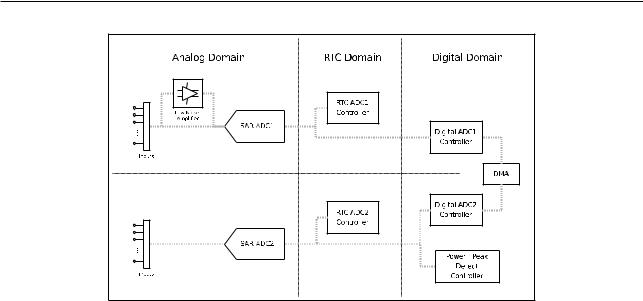
Figure 295. SAR ADC Depiction
29.3.2 Features
•Two SAR ADCs, with simultaneous sampling and conversion
•Up to five SAR ADC controllers for different purposes (e.g. high performance, low power or PWDET / PKDET).
•Up to 18 analog input pads
•12-bit, 11-bit, 10-bit, 9-bit configurable resolution
•DMA support (available on one controller)
•Multiple channel-scanning modes (available on two controllers)
•Operation during Deep-sleep (available on one controller)
•Controlled by a ULP coprocessor (available on two controllers)
29.3.3 Outline of Function
The SAR ADC module’s major components, and their interconnections, are shown in Figure 29-6.
Espressif Systems |
632 |
ESP32 TRM (Version 5.0) |
Submit Documentation Feedback
29 On-Chip Sensors and Analog Signal Processing
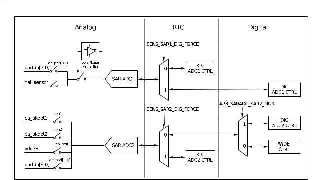
Figure 296. SAR ADC Outline of Function
Table 29-2 lists all the analog signals that may be sent to the SAR ADC module via the ADC channels.
Espressif Systems |
633 |
ESP32 TRM (Version 5.0) |
Submit Documentation Feedback

29 On-Chip Sensors and Analog Signal Processing
Table 292. Inputs of SAR ADC
Signal Name |
ADC Channel # |
Processed by |
|
VDET_2 |
7 |
|
|
|
|
|
|
VDET_1 |
6 |
|
|
|
|
|
|
32K_XN |
5 |
|
|
|
|
|
|
32K_XP |
4 |
SAR ADC1 |
|
|
|
||
SENSOR_VN |
3 |
||
|
|||
|
|
|
|
SENSOR_CAPN |
2 |
|
|
|
|
|
|
SENSOR_CAPP |
1 |
|
|
|
|
|
|
SENSOR_VP |
0 |
|
|
|
|
|
|
GPIO26 |
9 |
|
|
|
|
|
|
GPIO25 |
8 |
|
|
|
|
|
|
GPIO27 |
7 |
|
|
|
|
|
|
MTMS |
6 |
|
|
|
|
|
|
MTDI |
5 |
SAR ADC2 |
|
|
|
||
MTCK |
4 |
||
|
|||
|
|
|
|
MTDO |
3 |
|
|
|
|
|
|
GPIO2 |
2 |
|
|
|
|
|
|
GPIO0 |
1 |
|
|
|
|
|
|
GPIO4 |
0 |
|
|
|
|
|
Note:
• Some of the SAR ADC2 pins are used as strapping pins (GPIO0, GPIO2, and GPIO15), thus can not be used freely.
There are five ADC controllers in ESP32: RTC ADC1 CTRL, RTC ADC2 CTRL, DIG ADC1 CTRL, DIG ADC2 CTRL and PWDET CTRL. The differences between them are summarized in Table 29-3.
Table 293. ESP32 SAR ADC Controllers
|
RTC ADC1 |
RTC ADC2 |
DIG ADC1 |
DIG ADC2 |
PWDET |
DAC |
Y |
- |
- |
- |
- |
|
|
|
|
|
|
Support deep sleep |
Y |
Y |
- |
- |
- |
|
|
|
|
|
|
ULP coprocessor |
Y |
Y |
- |
- |
- |
|
|
|
|
|
|
PWDET/PKDET |
- |
- |
- |
- |
Y |
|
|
|
|
|
|
DMA |
- |
- |
Y |
- |
- |
|
|
|
|
|
|
29.3.4 RTC SAR ADC Controllers
The purpose of SAR ADC controllers in the RTC power domain – RTC ADC1 CTRL and RTC ADC2 CTRL – is to provide ADC measurement with minimal power consumption in a low frequency.
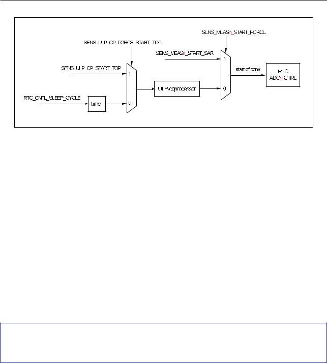
The outline of a single controller’s function is shown in Figure 29-7. For each controller, the start of analog-to- digital conversion can be triggered by register SENS_SAR_MEASn_START_SAR. The measurement’s result can be obtained from register SENS_SAR_MEASn_DATA_SAR.
The controllers are intertwined with the ULP coprocessor, as the ULP coprocessor has a built-in instruction to start an ADC measurement. In many cases, the controllers need to cooperate with the ULP coprocessor, e.g.:
Espressif Systems |
634 |
ESP32 TRM (Version 5.0) |
Submit Documentation Feedback
29 On-Chip Sensors and Analog Signal Processing
Figure 297. RTC SAR ADC Outline of Function
•when periodically monitoring a channel during deep sleep, where the ULP coprocessor is the only trigger source during this mode;
•when scanning channels continuously in a sequence. Continuous scanning or DMA is not supported by the controllers. However, it is possible with the help of the ULP coprocessor.
29.3.5 DIG SAR ADC Controllers
Compared to RTC SAR ADC controllers, DIG SAR ADC controllers have optimized performance and throughput.
Some of their features are:
•High performance; the clock is much faster, therefore, the sample rate is highly increased.
•Multiple-channel scanning mode; there is a pattern table that defines the measurement rule for each SAR ADC. The scanning mode can be configured as a single mode, double mode, or alternate mode.
•The scanning can be started by software or I2S.
•DMA support; an interrupt will be generated when scanning is finished.
Note:
We do not use the term “start of conversion” in this section, because there is no direct access to starting a single SAR analog-to-digital conversion. We use “start of scan” instead, which implies that we expect to scan a sequence of channels with DIG ADC controllers.
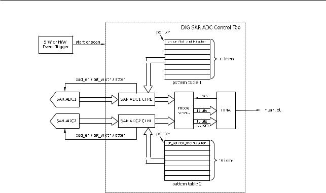
Figure 29-8 shows a diagram of DIG SAR ADC controllers.
Espressif Systems |
635 |
ESP32 TRM (Version 5.0) |
Submit Documentation Feedback
29 On-Chip Sensors and Analog Signal Processing
Figure 298. Diagram of DIG SAR ADC Controllers
The pattern tables contain the measurement rules mentioned above. Each table has 16 items which store information on channel selection, resolution and attenuation. When scanning starts, the controller reads measurement rules one-by-one from a pattern table. For each controller the scanning sequence includes 16 different rules at most, before repeating itself.
The 8-bit item (the pattern table register) is composed of three fields that contain channel, resolution and attenuation information, as shown in Table 29-4.
|
Table 294. Fields of the Pattern Table Register |
|||
|
|
|
|
|
|
|
Pattern Table Register [7:0] |
|
|
ch_sel[3:0] |
|
bit_width[1:0] |
atten[1:0] |
|
|
|
|
|
|
channel to be scanned |
|
resolution |
attenuation |
|
|
|
|
|
|
There are three scanning modes: single mode, double mode and alternate mode.
•Single mode: channels of either SAR ADC1 or SAR ADC2 will be scanned.
•Double mode: channels of SAR ADC1 and SAR ADC2 will be scanned simultaneously.
•Alternate mode: channels of SAR ADC1 and SAR ADC2 will be scanned alternately.
ESP32 supports up to a 12-bit SAR ADC resolution. The 16-bit data in DMA is composed of the ADC result and
some necessary information related to the scanning mode:
•For single mode, only 4-bit information on channel selection is added.
•For double mode or alternate mode, 4-bit information on channel selection is added plus one extra bit indicating which SAR ADC was selected.
Espressif Systems |
636 |
ESP32 TRM (Version 5.0) |
Submit Documentation Feedback