

- •1 System and Memory
- •1.1 Introduction
- •1.2 Features
- •1.3 Functional Description
- •1.3.1 Address Mapping
- •1.3.2 Embedded Memory
- •1.3.3 External Memory
- •1.3.5 Peripherals
- •2 Interrupt Matrix (INTERRUPT)
- •2.1 Overview
- •2.2 Features
- •2.3 Functional Description
- •2.3.1 Peripheral Interrupt Source
- •2.3.2 CPU Interrupt
- •2.3.3 Allocate Peripheral Interrupt Sources to Peripheral Interrupt on CPU
- •2.3.4 CPU NMI Interrupt Mask
- •2.3.5 Query Current Interrupt Status of Peripheral Interrupt Source
- •2.4 Registers
- •3 Reset and Clock
- •3.1 System Reset
- •3.1.1 Introduction
- •3.1.2 Reset Source
- •3.2 System Clock
- •3.2.1 Introduction
- •3.2.3 CPU Clock
- •3.2.4 Peripheral Clock
- •3.2.7 Audio PLL
- •3.3 Register Summary
- •3.4 Registers
- •4.1 Overview
- •4.2 Peripheral Input via GPIO Matrix
- •4.2.1 Summary
- •4.2.2 Functional Description
- •4.2.3 Simple GPIO Input
- •4.3 Peripheral Output via GPIO Matrix
- •4.3.1 Summary
- •4.3.3 Simple GPIO Output
- •4.4 Direct I/O via IO_MUX
- •4.4.1 Summary
- •4.4.2 Functional Description
- •4.5 RTC IO_MUX for Low Power and Analog I/O
- •4.5.1 Summary
- •4.5.2 Analog Function Description
- •4.7 Pad Hold Feature
- •4.8 I/O Pad Power Supplies
- •4.8.1 VDD_SDIO Power Domain
- •4.9 Peripheral Signal List
- •4.10 IO_MUX Pad List
- •4.11 RTC_MUX Pin List
- •4.12 Register Summary
- •4.12.1 GPIO Matrix Register Summary
- •4.12.2 IO MUX Register Summary
- •4.12.3 RTC IO MUX Register Summary
- •4.13 Registers
- •4.13.1 GPIO Matrix Registers
- •4.13.2 IO MUX Registers
- •4.13.3 RTC IO MUX Registers
- •5 DPort Registers
- •5.1 Introduction
- •5.2 Features
- •5.3 Functional Description
- •5.3.1 System and Memory Register
- •5.3.2 Reset and Clock Registers
- •5.3.3 Interrupt Matrix Register
- •5.3.4 DMA Registers
- •5.3.5 MPU/MMU Registers
- •5.3.7 Peripheral Clock Gating and Reset
- •5.4 Register Summary
- •5.5 Registers
- •6 DMA Controller (DMA)
- •6.1 Overview
- •6.2 Features
- •6.3 Functional Description
- •6.3.1 DMA Engine Architecture
- •6.3.2 Linked List
- •6.4 UART DMA (UDMA)
- •7 SPI Controller (SPI)
- •7.1 Overview
- •7.5 Parallel QSPI
- •7.5.1 Communication Format of Parallel QSPI
- •7.6.1 SPI Interrupts
- •7.6.2 DMA Interrupts
- •7.7 Register Summary
- •7.8 Registers
- •8 SDIO Slave Controller
- •8.1 Overview
- •8.2 Features
- •8.3 Functional Description
- •8.3.1 SDIO Slave Block Diagram
- •8.3.3 Register Access
- •8.3.6 SDIO Bus Timing
- •8.3.7 Interrupt
- •8.4 Register Summary
- •8.5 SLC Registers
- •8.6 SLC Host Registers
- •8.7 HINF Registers
- •9 SD/MMC Host Controller
- •9.1 Overview
- •9.2 Features
- •9.3 SD/MMC External Interface Signals
- •9.4 Functional Description
- •9.4.1 SD/MMC Host Controller Architecture
- •9.4.2 Command Path
- •9.4.3 Data Path
- •9.5 Software Restrictions for Proper CIU Operation
- •9.6 RAM for Receiving and Sending Data
- •9.6.1 Transmit RAM Module
- •9.6.2 Receive RAM Module
- •9.8 The Structure of a Linked List
- •9.9 Initialization
- •9.9.1 DMAC Initialization
- •9.9.2 DMAC Transmission Initialization
- •9.9.3 DMAC Reception Initialization
- •9.11 Interrupt
- •9.12 Register Summary
- •9.13 Registers
- •10 Ethernet Media Access Controller (MAC)
- •10.1 Overview
- •10.2 EMAC_CORE
- •10.2.1 Transmit Operation
- •10.2.2 Receive Operation
- •10.3 MAC Interrupt Controller
- •10.4 MAC Address Filtering
- •10.4.1 Unicast Destination Address Filtering
- •10.4.2 Multicast Destination Address Filtering
- •10.4.3 Broadcast Address Filtering
- •10.4.4 Unicast Source Address Filtering
- •10.4.5 Inverse Filtering Operation
- •10.4.6 Good Transmitted Frames and Received Frames
- •10.5 EMAC_MTL (MAC Transaction Layer)
- •10.6 PHY Interface
- •10.6.1 MII (Media Independent Interface)
- •10.6.3 Station Management Agent (SMA) Interface
- •10.6.4 RMII Timing
- •10.7 Ethernet DMA Features
- •10.8 Linked List Descriptors
- •10.8.1 Transmit Descriptors
- •10.8.2 Receive Descriptors
- •10.9 Register Summary
- •10.10 Registers
- •11 I2C Controller (I2C)
- •11.1 Overview
- •11.2 Features
- •11.3 Functional Description
- •11.3.1 Introduction
- •11.3.2 Architecture
- •11.3.3 I2C Bus Timing
- •11.3.7 Interrupts
- •11.4 Register Summary
- •11.5 Registers
- •12 I2S Controller (I2S)
- •12.1 Overview
- •12.2 Features
- •12.3 The Clock of I2S Module
- •12.4 I2S Mode
- •12.4.1 Supported Audio Standards
- •12.4.2 Module Reset
- •12.4.3 FIFO Operation
- •12.4.5 Receiving Data
- •12.5.1 LCD Master Transmitting Mode
- •12.5.2 Camera Slave Receiving Mode
- •12.5.3 ADC/DAC mode
- •12.6 I2S Interrupts
- •12.6.1 FIFO Interrupts
- •12.6.2 DMA Interrupts
- •12.7 Register Summary
- •12.8 Registers
- •13 UART Controller (UART)
- •13.1 Overview
- •13.2 UART Features
- •13.3 Functional Description
- •13.3.1 Introduction
- •13.3.3 UART RAM
- •13.3.5 UART Data Frame
- •13.3.7 Flow Control
- •13.3.8 UART DMA
- •13.3.9 UART Interrupts
- •13.3.10 UHCI Interrupts
- •13.4 Register Summary
- •13.4.1 UART Register Summary
- •13.5 Registers
- •13.5.1 UART Registers
- •13.5.2 UHCI Registers
- •14 LED PWM Controller (LEDC)
- •14.1 Introduction
- •14.2 Functional Description
- •14.2.1 Architecture
- •14.2.3 Channels
- •14.2.4 Interrupts
- •14.3 Register Summary
- •14.4 Registers
- •15 Remote Control Peripheral (RMT)
- •15.1 Introduction
- •15.2 Functional Description
- •15.2.1 RMT Architecture
- •15.2.3 Clock
- •15.2.4 Transmitter
- •15.2.5 Receiver
- •15.2.6 Interrupts
- •15.3 Register Summary
- •15.4 Registers
- •16 Motor Control PWM (PWM)
- •16.1 Introduction
- •16.2 Features
- •16.3 Submodules
- •16.3.1 Overview
- •16.3.2 PWM Timer Submodule
- •16.3.3 PWM Operator Submodule
- •16.3.4 Capture Submodule
- •16.4 Register Summary
- •16.5 Registers
- •17 Pulse Count Controller (PCNT)
- •17.1 Overview
- •17.2 Functional Description
- •17.2.1 Architecture
- •17.2.2 Counter Channel Inputs
- •17.2.3 Watchpoints
- •17.2.4 Examples
- •17.2.5 Interrupts
- •18 Timer Group (TIMG)
- •18.1 Introduction
- •18.2 Functional Description
- •18.2.2 64-bit Time-base Counter
- •18.2.3 Alarm Generation
- •18.2.4 MWDT
- •18.2.5 Interrupts
- •18.3 Register Summary
- •18.4 Registers
- •19 Watchdog Timers (WDT)
- •19.1 Introduction
- •19.2 Features
- •19.3 Functional Description
- •19.3.1 Clock
- •20 eFuse Controller
- •20.1 Introduction
- •20.2 Features
- •20.3 Functional Description
- •20.3.1 Structure
- •20.3.3 Software Reading of System Parameters
- •20.3.4 The Use of System Parameters by Hardware Modules
- •20.3.5 Interrupts
- •20.4 Register Summary
- •20.5 Registers
- •21 Two-wire Automotive Interface (TWAI)
- •21.1 Overview
- •21.2 Features
- •21.3 Functional Protocol
- •21.3.1 TWAI Properties
- •21.3.2 TWAI Messages
- •21.3.3 TWAI Errors
- •21.3.4 TWAI Bit Timing
- •21.4 Architectural Overview
- •21.4.1 Registers Block
- •21.4.2 Bit Stream Processor
- •21.4.3 Error Management Logic
- •21.4.4 Bit Timing Logic
- •21.4.5 Acceptance Filter
- •21.5 Functional Description
- •21.5.1 Modes
- •21.5.2 Bit Timing
- •21.5.3 Interrupt Management
- •21.5.4 Transmit and Receive Buffers
- •21.5.5 Receive FIFO and Data Overruns
- •21.5.6 Acceptance Filter
- •21.5.8 Error Code Capture
- •21.5.9 Arbitration Lost Capture
- •21.6 Register Summary
- •21.7 Registers
- •22 AES Accelerator (AES)
- •22.1 Introduction
- •22.2 Features
- •22.3 Functional Description
- •22.3.1 AES Algorithm Operations
- •22.3.2 Key, Plaintext and Ciphertext
- •22.3.3 Endianness
- •22.3.4 Encryption and Decryption Operations
- •22.3.5 Speed
- •22.4 Register Summary
- •22.5 Registers
- •23 SHA Accelerator (SHA)
- •23.1 Introduction
- •23.2 Features
- •23.3 Functional Description
- •23.3.1 Padding and Parsing the Message
- •23.3.2 Message Digest
- •23.3.3 Hash Operation
- •23.3.4 Speed
- •23.4 Register Summary
- •23.5 Registers
- •24 RSA Accelerator (RSA)
- •24.1 Introduction
- •24.2 Features
- •24.3 Functional Description
- •24.3.1 Initialization
- •24.3.2 Large Number Modular Exponentiation
- •24.3.4 Large Number Multiplication
- •24.4 Register Summary
- •24.5 Registers
- •25 Random Number Generator (RNG)
- •25.1 Introduction
- •25.2 Feature
- •25.3 Functional Description
- •25.5 Register Summary
- •25.6 Register
- •26 External Memory Encryption and Decryption (FLASH)
- •26.1 Overview
- •26.2 Features
- •26.3 Functional Description
- •26.3.1 Key Generator
- •26.3.2 Flash Encryption Block
- •26.3.3 Flash Decryption Block
- •26.4 Register Summary
- •26.5 Register
- •27 Memory Management and Protection Units (MMU, MPU)
- •27.1 Introduction
- •27.2 Features
- •27.3 Functional Description
- •27.3.1 PID Controller
- •28 Process ID Controller (PID)
- •28.1 Overview
- •28.2 Features
- •28.3 Functional Description
- •28.3.1 Interrupt Identification
- •28.3.2 Information Recording
- •28.3.3 Proactive Process Switching
- •28.4 Register Summary
- •28.5 Registers
- •29 On-Chip Sensors and Analog Signal Processing
- •29.1 Introduction
- •29.2 Capacitive Touch Sensor
- •29.2.1 Introduction
- •29.2.2 Features
- •29.2.3 Available GPIOs
- •29.2.4 Functional Description
- •29.2.5 Touch FSM
- •29.3.1 Introduction
- •29.3.2 Features
- •29.3.3 Outline of Function
- •29.3.4 RTC SAR ADC Controllers
- •29.3.5 DIG SAR ADC Controllers
- •29.4.1 Introduction
- •29.4.2 Features
- •29.4.4 Cosine Waveform Generator
- •29.5 Register Summary
- •29.5.1 Sensors
- •29.5.2 Advanced Peripheral Bus
- •29.6 Registers
- •29.6.1 Sensors
- •29.6.2 Advanced Peripheral Bus
- •30 ULP Coprocessor (ULP)
- •30.1 Introduction
- •30.2 Features
- •30.4 Instruction Set
- •30.4.2 ST – Store Data in Memory
- •30.4.3 LD – Load Data from Memory
- •30.4.4 JUMP – Jump to an Absolute Address
- •30.4.5 JUMPR – Jump to a Relative Offset (Conditional upon R0)
- •30.4.7 HALT – End the Program
- •30.4.8 WAKE – Wake up the Chip
- •30.4.10 WAIT – Wait for a Number of Cycles
- •30.4.12 I2C_RD/I2C_WR – Read/Write I²C
- •30.4.13 REG_RD – Read from Peripheral Register
- •30.5 ULP Program Execution
- •30.6 RTC_I2C Controller
- •30.6.1 Configuring RTC_I2C
- •30.6.2 Using RTC_I2C
- •30.7 Register Summary
- •30.7.1 SENS_ULP Address Space
- •30.7.2 RTC_I2C Address Space
- •30.8 Registers
- •30.8.1 SENS_ULP Address Space
- •30.8.2 RTC_I2C Address Space
- •31 Low-Power Management (RTC_CNTL)
- •31.1 Introduction
- •31.2 Features
- •31.3 Functional Description
- •31.3.2 Digital Core Voltage Regulator
- •31.3.4 Flash Voltage Regulator
- •31.3.5 Brownout Detector
- •31.3.6 RTC Module
- •31.3.9 Predefined Power Modes
- •31.3.10 Wakeup Source
- •31.3.12 RTC Timer
- •31.3.13 RTC Boot
- •31.4 Register Summary
- •31.5 Registers
- •Glossary
- •Abbreviations for Peripherals
- •Abbreviations for Registers
- •Revision History

27 Memory Management and Protection Units (MMU, MPU)
27 Memory Management and Protection Units (MMU, MPU)
27.1Introduction
Every peripheral and memory section in the ESP32 is accessed through either an MMU (Memory Management Unit) or an MPU (Memory Protection Unit). An MPU can allow or disallow the access of an application to a memory range or peripheral, depending on what kind of permission the OS has given to that particular application. An MMU can perform the same operation, as well as a virtual-to-physical memory address translation. This can be used to map an internal or external memory range to a certain virtual memory area. These mappings can be applicationspecific. Therefore, each application can be adjusted and have the memory configuration that is necessary for it to run properly. To differentiate between the OS and applications, there are eight Process Identifiers (or PIDs) that each application, or OS, can run. Furthermore, each application, or OS, is equipped with their own sets of mappings and rights.
27.2Features
•Eight processes in each of the PRO_CPU and APP_CPU
•MPU/MMU management of on-chip memories, off-chip memories, and peripherals, based on process ID
•On-chip memory management by MPU/MMU
•Off-chip memory management by MMU
•Peripheral management by MPU
27.3Functional Description
27.3.1 PID Controller
In the ESP32, a PID controller acts as an indicator that signals the MMU/MPU the owner PID of the code that is currently running. The intention is that the OS updates the PID in the PID controller every time it switches context to another application. The PID controller can detect interrupts and automatically switch PIDs to that of the OS, if so configured.
There are two peripheral PID controllers in the system, one for each of the two CPUs in the ESP32. Having a PID controller per CPU allows running different processes on different CPUs, if so desired.
27.3.2 MPU/MMU
The MPU and MMU manage on-chip memories, off-chip memories, and peripherals. To do this they are based on the process of accessing the peripheral or memory region. More specifically, when a code tries to access a MMU/MPU-protected memory region or peripheral, the MMU or MPU will receive the PID from the PID generator that is associated with the CPU on which the process is running.
For on-chip memory and peripherals, the decisions the MMU and MPU make are only based on this PID, whereas the specific CPU the code is running on is not taken into account. Subsequently, the MMU/MPU configuration for the internal memory and peripherals allows entries only for the eight different PIDs. In contrast, the MMU moderating access to the external memory takes not only the PID into account, but also the CPU the request is coming from. This means that MMUs have configuration options for every PID when running on the APP_CPU, as well as every PID when running on the PRO_CPU. While, in practice, accesses from both CPUs will be configured to have the same result for a specific process, doing so is not a hardware requirement.
Espressif Systems |
603 |
ESP32 TRM (Version 5.0) |
Submit Documentation Feedback

27 Memory Management and Protection Units (MMU, MPU)
The decision an MPU can make, based on this information, is to allow or deny a process to access the memory region or peripheral. An MMU has the same function, but additionally it redirects the virtual memory access, which the process acquired, into a physical memory access that can possibly reach out an entirely different physical memory region. This way, MMU-governed memory can be remapped on a process-by-process basis.
27.3.2.1 Embedded Memory
The on-chip memory is governed by fixed-function MPUs, configurable MPUs, and MMUs:
Table 271. MPU and MMU Structure for Internal Memory
Name |
Size |
Address range |
Governed by |
||
From |
To |
||||
|
|
|
|||
ROM0 |
384 KB |
0x4000_0000 |
0x4005_FFFF |
Static MPU |
|
|
|
|
|
|
|
ROM1 |
64 KB |
0x3FF9_0000 |
0x3FF9_FFFF |
Static MPU |
|
|
|
|
|
|
|
SRAM0 |
64 KB |
0x4007_0000 |
0x4007_FFFF |
Static MPU |
|
128 KB |
0x4008_0000 |
0x4009_FFFF |
SRAM0 MMU |
||
|
|||||
|
|
|
|
|
|
|
128 KB |
0x3FFE_0000 |
0x3FFF_FFFF |
Static MPU |
|
SRAM1 (aliases) |
128 KB |
0x400A_0000 |
0x400B_FFFF |
Static MPU |
|
|
32 KB |
0x4000_0000 |
0x4000_7FFF |
Static MPU |
|
|
|
|
|
|
|
SRAM2 |
72 KB |
0x3FFA_E000 |
0x3FFB_FFFF |
Static MPU |
|
128 KB |
0x3FFC_0000 |
0x3FFD_FFFF |
SRAM2 MMU |
||
|
|||||
|
|
|
|
|
|
RTC FAST (aliases) |
8 KB |
0x3FF8_0000 |
0x3FF8_1FFF |
RTC FAST MPU |
|
8 KB |
0x400C_0000 |
0x400C_1FFF |
RTC FAST MPU |
||
|
|||||
|
|
|
|
|
|
RTC SLOW |
8 KB |
0x5000_0000 |
0x5000_1FFF |
RTC SLOW MPU |
|
|
|
|
|
|
|
Static MPUs
ROM0, ROM1, the lower 64 KB of SRAM0, SRAM1 and the lower 72 KB of SRAM2 are governed by a static MPU. The behaviour of these MPUs are hardwired and cannot be configured by software. They moderate access to the memory region solely through the PID of the current process. When the PID of the process is 0 or 1, the memory can be read (and written when it is RAM) using the addresses specified in Table 27-1. When it is 2 ~ 7, the memory cannot be accessed.
RTC FAST & RTC SLOW MPU
The 8 KB RTC FAST Memory as well as the 8 KB of RTC SLOW Memory are governed by two configurable MPUs. The MPUs can be configured to allow or deny access to each individual PID, using the RTC_CNTL_RTC_PID_ CONFIG_REG and DPORT_AHBLITE_MPU_TABLE_RTC_REG registers. Setting a bit in these registers will allow the corresponding PID to read or write from the memory; clearing the bit disallows access. Access for PID 0 and 1 to RTC SLOW memory cannot be configured and is always enabled. Table 27-2 and 27-3 define the bit-to-PID mappings of the registers.
Espressif Systems |
604 |
ESP32 TRM (Version 5.0) |
Submit Documentation Feedback

27 Memory Management and Protection Units (MMU, MPU)
Table 272. MPU for RTC FAST Memory
|
|
|
Boundary address |
|
Authority |
|||||||
Size |
|
Low |
|
High |
|
|
PID |
|
|
|||
|
|
|
|
|
RTC_CNTL_RTC_PID_CONFIG bit |
|
|
|||||
|
|
|
|
|
|
|
|
|
|
|
|
|
8 KB |
|
0x3FF8_0000 |
0x3FF8_1FFF |
|
0 1 2 3 4 5 6 7 |
|
|
|||||
|
|
|
|
|
|
|
|
|
|
|
|
|
8 KB |
|
0x400C_0000 |
0x400C_1FFF |
|
0 1 2 3 4 5 6 7 |
|
|
|||||
|
|
|
|
|
|
|
|
|
|
|
|
|
|
|
|
Table 273. MPU for RTC SLOW Memory |
|||||||||
|
|
|
|
|
|
|
|
|
|
|
|
|
|
|
Boundary address |
|
|
|
|
|
|
Authority |
|||
Size |
Low |
High |
|
PID = 0/1 |
|
|
|
|
PID |
|
||
|
|
|
|
DPORT_AHBLITE_MPU_TABLE_RTC_REG bit |
|
|||||||
|
|
|
|
|
|
|
|
|
||||
8 KB |
0x5000_0000 |
0x5000_1FFF |
Read/Write |
|
2 3 4 5 6 7 |
|
|
|||||
|
0 1 2 3 4 5 |
|
|
|||||||||
|
|
|
|
|
|
|
|
|
|
|||
|
|
|
|
|
|
|
|
|
|
|
|
|
Register RTC_CNTL_RTC_PID_CONFIG_REG is part of the RTC peripheral and can only be modified by processes with a PID of 0; register DPORT_AHBLITE_MPU_TABLE_RTC_REG is a Dport register and can be changed by processes with a PID of 0 or 1.
SRAM0 and SRAM2 upper 128 KB MMUs
Both the upper 128 KB of SRAM0 and the upper 128 KB of SRAM2 are governed by an MMU. Not only can these MMUs allow or deny access to the memory they govern (just like the MPUs do), but they are also capable of translating the address a CPU reads from or writes to (which is a virtual address) to a possibly different address in memory (the physical address).
In order to accomplish this, the internal RAM MMUs divide the memory range they govern into 16 pages. The page size is configurable as 8 KB, 4 KB and 2 KB. When the page size is 8 KB, the 16 pages span the entire 128 KB memory region; when the page size is 4 KB or 2 KB, a non-MMU-covered region of 64 or 96 KB, respectively, will exist at the end of the memory space. Similar to the virtual and physical addresses, it is also possible to imagine the pages as having a virtual and physical component. The MMU can convert an address within a virtual page to an address within a physical page.
For PID 0 and 1, this mapping is 1-to-1, meaning that a read from or write to a certain virtual page will always be converted to a read from or write to the exact same physical page. This allows an operating system, running under PID 0 and/or 1, to always have access to the entire physical memory range.
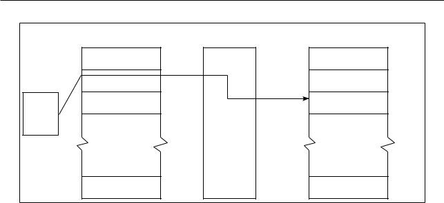
For PID 2 to 7, however, every virtual page can be reconfigured, on a per-PID basis, to map to a different physical page. This way, reads and writes to an offset within a virtual page get translated into reads and writes to the same offset within a different physical page. This is illustrated in Figure 27-1: the CPU (running a process with a PID between 2 to 7) tries to access memory address 0x3FFC_2345. This address is within the virtual Page 1 memory region, at offset 0x0345. The MMU is instructed that for this particular PID, it should translate an access to virtual page 1 into physical Page 2. This causes the memory access to be redirected to the same offset as the virtual memory access, yet in Page 2, which results in the effective access of physical memory address 0x3FFC_4345. The page size in this example is 8 KB.
Espressif Systems |
605 |
ESP32 TRM (Version 5.0) |
Submit Documentation Feedback
27 Memory Management and Protection Units (MMU, MPU)
CPU |
VIRTUAL |
MMU |
|
PHYSICAL |
|
|
3FFC_0000 |
|
3FFC_0000 |
|
PAGE 0 |
|
|
PAGE 0 |
3FFC_2345 |
|
3FFC_2000 |
|
3FFC_2000 |
PAGE 1 |
|
|
PAGE 1 |
|
|
|
3FFC_4000 |
3FFC_4345 |
3FFC_4000 |
|
PAGE 2 |
|
PAGE 2 |
|
|
|
|
||
|
|
3FFC_6000 |
|
3FFC_6000 |
|
|
3FFD_E000 |
|
3FFD_E000 |
|
PAGE 15 |
|
|
PAGE 15 |
|
|
3FFE_0000 |
|
3FFE_0000 |
Figure 271. MMU Access Example
Table 274. Page Mode of MMU for the Remaining 128 KB of Internal SRAM0 and SRAM2
DPORT_IMMU_PAGE_MODE |
DPORT_DMMU_PAGE_MODE |
Page size |
0 |
0 |
8 KB |
|
|
|
1 |
1 |
4 KB |
|
|
|
2 |
2 |
2 KB |
|
|
|
NonMMU Governed Memory
For the MMU-managed region of SRAM0 and SRAM2, the page size is configurable as 8 KB, 4 KB and 2 KB. The configuration is done by setting the DPORT_IMMU_PAGE_MODE (for SRAM0) and DPORT_DMMU_PAGE_MODE (for SRAM2) bits in registers DPORT_IMMU_PAGE_MODE_REG and DPORT_DMMU_PAGE_MODE_REG, as detailed in Table 27-4. Because the number of pages for either region is fixed at 16, the total amount of memory covered by these pages is 128 KB when 8 KB pages are selected, 64 KB when 4 KB pages are selected, and 32 KB when 2 KB pages are selected. This implies that for 8 KB pages, the entire MMU-managed range is used, but for the other page sizes there will be a part of the 128 KB memory that will not be governed by the MMU settings. Concretely, for a page size of 4 KB, these regions are 0x4009_0000 to 0x4009_FFFF and 0x3FFD_0000 to 0x3FFD_FFFF; for a page size of 2 KB, the regions are 0x4008_8000 to 0x4009_FFFF and 0x3FFC_8000 to 0x3FFD_FFFF. These ranges are readable and writable by processes with a PID of 0 or 1; processes with other PIDs cannot access this memory.
The layout of the pages in memory space is linear, namely, an SRAM0 MMU page n covers address space
0x40080000 + (pagesize n) to 0x40080000 + (pagesize (n + 1) − 1); similarily, an SRAM2 MMU page n covers
0x3F F C0000 + (pagesize n) to 0x3F F C0000 + (pagesize (n + 1) −1). Tables 27-5 and 27-6 show the resulting addresses in full.
Espressif Systems |
606 |
ESP32 TRM (Version 5.0) |
Submit Documentation Feedback

27 Memory Management and Protection Units (MMU, MPU)
Table 275. Page Boundaries for SRAM0 MMU
Page |
8 KB Pages |
4 KB Pages |
2 KB Pages |
||||
Bottom |
|
Top |
Bottom |
Top |
Bottom |
Top |
|
|
|
||||||
0 |
40080000 |
|
40081FFF |
40080000 |
40080FFF |
40080000 |
400807FF |
|
|
|
|
|
|
|
|
1 |
40082000 |
|
40083FFF |
40081000 |
40081FFF |
40080800 |
40080FFF |
|
|
|
|
|
|
|
|
2 |
40084000 |
|
40085FFF |
40082000 |
40082FFF |
40081000 |
400817FF |
|
|
|
|
|
|
|
|
3 |
40086000 |
|
40087FFF |
40083000 |
40083FFF |
40081800 |
40081FFF |
|
|
|
|
|
|
|
|
4 |
40088000 |
|
40089FFF |
40084000 |
40084FFF |
40082000 |
400827FF |
|
|
|
|
|
|
|
|
5 |
4008A000 |
|
4008BFFF |
40085000 |
40085FFF |
40082800 |
40082FFF |
|
|
|
|
|
|
|
|
6 |
4008C000 |
|
4008DFFF |
40086000 |
40086FFF |
40083000 |
400837FF |
|
|
|
|
|
|
|
|
7 |
4008E000 |
|
4008FFFF |
40087000 |
40087FFF |
40083800 |
40083FFF |
|
|
|
|
|
|
|
|
8 |
40090000 |
|
40091FFF |
40088000 |
40088FFF |
40084000 |
400847FF |
|
|
|
|
|
|
|
|
9 |
40092000 |
|
40093FFF |
40089000 |
40089FFF |
40084800 |
40084FFF |
|
|
|
|
|
|
|
|
10 |
40094000 |
|
40095FFF |
4008A000 |
4008AFFF |
40085000 |
400857FF |
|
|
|
|
|
|
|
|
11 |
40096000 |
|
40097FFF |
4008B000 |
4008BFFF |
40085800 |
40085FFF |
|
|
|
|
|
|
|
|
12 |
40098000 |
|
40099FFF |
4008C000 |
4008CFFF |
40086000 |
400867FF |
|
|
|
|
|
|
|
|
13 |
4009A000 |
|
4009BFFF |
4008D000 |
4008DFFF |
40086800 |
40086FFF |
|
|
|
|
|
|
|
|
14 |
4009C000 |
|
4009DFFF |
4008E000 |
4008EFFF |
40087000 |
400877FF |
|
|
|
|
|
|
|
|
15 |
4009E000 |
|
4009FFFF |
4008F000 |
4008FFFF |
40087800 |
40087FFF |
|
|
|
|
|
|
|
|
Rest |
- |
- |
40090000 |
4009FFFF |
4008800 |
4009FFFF |
|
|
|
|
|
|
|
|
|
|
|
|
Table 276. Page Boundaries for SRAM2 MMU |
|
|||
|
|
|
|
||||
Page |
8 KB Pages |
4 KB Pages |
2 KB Pages |
||||
Bottom |
|
Top |
Bottom |
Top |
Bottom |
Top |
|
|
|
||||||
0 |
3FFC0000 |
|
3FFC1FFF |
3FFC0000 |
3FFC0FFF |
3FFC0000 |
3FFC07FF |
|
|
|
|
|
|
|
|
1 |
3FFC2000 |
|
3FFC3FFF |
3FFC1000 |
3FFC1FFF |
3FFC0800 |
3FFC0FFF |
|
|
|
|
|
|
|
|
2 |
3FFC4000 |
|
3FFC5FFF |
3FFC2000 |
3FFC2FFF |
3FFC1000 |
3FFC17FF |
|
|
|
|
|
|
|
|
3 |
3FFC6000 |
|
3FFC7FFF |
3FFC3000 |
3FFC3FFF |
3FFC1800 |
3FFC1FFF |
|
|
|
|
|
|
|
|
4 |
3FFC8000 |
|
3FFC9FFF |
3FFC4000 |
3FFC4FFF |
3FFC2000 |
3FFC27FF |
|
|
|
|
|
|
|
|
5 |
3FFCA000 |
|
3FFCBFFF |
3FFC5000 |
3FFC5FFF |
3FFC2800 |
3FFC2FFF |
|
|
|
|
|
|
|
|
6 |
3FFCC000 |
|
3FFCDFFF |
3FFC6000 |
3FFC6FFF |
3FFC3000 |
3FFC37FF |
|
|
|
|
|
|
|
|
7 |
3FFCE000 |
|
3FFCFFFF |
3FFC7000 |
3FFC7FFF |
3FFC3800 |
3FFC3FFF |
|
|
|
|
|
|
|
|
8 |
3FFD0000 |
|
3FFD1FFF |
3FFC8000 |
3FFC8FFF |
3FFC4000 |
3FFC47FF |
|
|
|
|
|
|
|
|
9 |
3FFD2000 |
|
3FFD3FFF |
3FFC9000 |
3FFC9FFF |
3FFC4800 |
3FFC4FFF |
|
|
|
|
|
|
|
|
10 |
3FFD4000 |
|
3FFD5FFF |
3FFCA000 |
3FFCAFFF |
3FFC5000 |
3FFC57FF |
|
|
|
|
|
|
|
|
11 |
3FFD6000 |
|
3FFD7FFF |
3FFCB000 |
3FFCBFFF |
3FFC5800 |
3FFC5FFF |
|
|
|
|
|
|
|
|
12 |
3FFD8000 |
|
3FFD9FFF |
3FFCC000 |
3FFCCFFF |
3FFC6000 |
3FFC67FF |
|
|
|
|
|
|
|
|
13 |
3FFDA000 |
|
3FFDBFFF |
3FFCD000 |
3FFCDFFF |
3FFC6800 |
3FFC6FFF |
|
|
|
|
|
|
|
|
14 |
3FFDC000 |
|
3FFDDFFF |
3FFCE000 |
3FFCEFFF |
3FFC7000 |
3FFC77FF |
|
|
|
|
|
|
|
|
15 |
3FFDE000 |
|
3FFDFFFF |
3FFCF000 |
3FFCFFFF |
3FFC7800 |
3FFC7FFF |
|
|
|
|
|
|
|
|
Rest |
- |
- |
3FFD0000 |
3FFDFFFF |
3FFC8000 |
3FFDFFFF |
|
|
|
|
|
|
|
|
|
Espressif Systems |
607 |
ESP32 TRM (Version 5.0) |
Submit Documentation Feedback

27 Memory Management and Protection Units (MMU, MPU)
MMU Mapping
For each of the SRAM0 and SRAM2 MMUs, access rights and virtual to physical page mapping are done by a set of 16 registers. In contrast to most of the other MMUs, each register controls a physical page, not a virtual one. These registers control which of the PIDs have access to the physical memory, as well as which virtual page maps to this physical page. The bits in the register are described in Table 27-7. Keep in mind that these registers only govern accesses from processes with PID 2 to 7; PID 0 and 1 always have full read and write access to all pages and no virtual-to-physical mapping is done. In other words, if a process with a PID of 0 or 1 accesses virtual page x, the access will always go to physical page x, regardless of these register settings. These registers, as well as the page size selection registers DPORT_IMMU_PAGE_MODE_REG and DPORT_DMMU_PAGE_MODE_REG, are only writable from a process with PID 0 or 1.
Table 277. DPORT_DMMU_TABLEn_REG & DPORT_IMMU_TABLEn_REG
[6:4] |
Access rights for PID 2 ~ 7 |
0 |
None of PIDs 2 ~ 7 have access. |
|
|
1 |
All of PIDs 2 ~ 7 have access. |
|
|
2 |
Only PID 2 has access. |
|
|
3 |
Only PID 3 has access. |
|
|
4 |
Only PID 4 has access. |
|
|
5 |
Only PID 5 has access. |
|
|
6 |
Only PID 6 has access. |
|
|
7 |
Only PID 7 has access. |
|
|
[3:0] |
Address authority |
0x00 |
Virtual page 0 accesses this physical page. |
|
|
0x01 |
Virtual page 1 accesses this physical page. |
|
|
0x02 |
Virtual page 2 accesses this physical page. |
|
|
0x03 |
Virtual page 3 accesses this physical page. |
|
|
0x04 |
Virtual page 4 accesses this physical page. |
|
|
0x05 |
Virtual page 5 accesses this physical page. |
|
|
0x06 |
Virtual page 6 accesses this physical page. |
|
|
0x07 |
Virtual page 7 accesses this physical page. |
|
|
0x08 |
Virtual page 8 accesses this physical page. |
|
|
0x09 |
Virtual page 9 accesses this physical page. |
|
|
0x10 |
Virtual page 10 accesses this physical page. |
|
|
0x11 |
Virtual page 11 accesses this physical page. |
|
|
0x12 |
Virtual page 12 accesses this physical page. |
|
|
0x13 |
Virtual page 13 accesses this physical page. |
|
|
0x14 |
Virtual page 14 accesses this physical page. |
|
|
0x15 |
Virtual page 15 accesses this physical page. |
|
|
Differences Between SRAM0 and SRAM2 MMU
The memory governed by the SRAM0 MMU is accessed through the processors I-bus, while the processor accesses the memory governed by the SRAM2 MMU through the D-bus. Thus, the normal envisioned use is for the code to be stored in the SRAM0 MMU pages and data in the MMU pages of SRAM2. In general, applications running under a PID of 2 to 7 are not expected to modify their own code, because for these PIDs access to the MMU pages of SRAM0 is read-only. These applications must, however, be able to modify their data section, so that they are allowed to read as well as write MMU pages located in SRAM2. As stated before, processes running under PID 0 or 1 always have full read-and-write access to both memory ranges.
DMA MPU
Applications may want to configure the DMA to send data straight from or to the peripherals they can control. With access to DMA, a malicious process may also be able to copy data from or to a region it cannot normally access. In order to be secure against that scenario, there is a DMA MPU which can be used to disallow DMA transfers
Espressif Systems |
608 |
ESP32 TRM (Version 5.0) |
Submit Documentation Feedback

27 Memory Management and Protection Units (MMU, MPU)
from memory regions with sensitive data in them.
For each 8 KB region in the SRAM1 and SRAM2 regions, there is a bit in the DPORT_AHB_MPU_TABLE_n_REG registers which tells the MPU to either allow or disallow DMA access to this region. The DMA MPU uses only these bits to decide if a DMA transfer can be started; the PID of the process is not a factor. This means that when the OS wants to restrict its processes in a heterogenous fashion, it will need to re-load these registers with the values applicable to the process to be run on every context switch.
The register bits that govern access to the 8 KB regions are detailed in Table 27-8. When a register bit is set, DMA can read/write the corresponding 8 KB memory range. When the bit is cleared, access to that memory range is denied.
Table 278. MPU for DMA
Size |
Boundary address |
|
Authority |
|
|
Low |
High |
|
Register |
Bit |
|
|
|
||||
|
|
Internal SRAM 2 |
|
||
8 KB |
0x3FFA_E000 |
0x3FFA_FFFF |
|
DPORT_AHB_MPU_TABLE_0_REG |
0 |
|
|
|
|
|
|
8 KB |
0x3FFB_0000 |
0x3FFB_1FFF |
|
DPORT_AHB_MPU_TABLE_0_REG |
1 |
|
|
|
|
|
|
8 KB |
0x3FFB_2000 |
0x3FFB_3FFF |
|
DPORT_AHB_MPU_TABLE_0_REG |
2 |
|
|
|
|
|
|
8 KB |
0x3FFB_4000 |
0x3FFB_5FFF |
|
DPORT_AHB_MPU_TABLE_0_REG |
3 |
|
|
|
|
|
|
8 KB |
0x3FFB_6000 |
0x3FFB_7FFF |
|
DPORT_AHB_MPU_TABLE_0_REG |
4 |
|
|
|
|
|
|
8 KB |
0x3FFB_8000 |
0x3FFB_9FFF |
|
DPORT_AHB_MPU_TABLE_0_REG |
5 |
|
|
|
|
|
|
8 KB |
0x3FFB_A000 |
0x3FFB_BFFF |
|
DPORT_AHB_MPU_TABLE_0_REG |
6 |
|
|
|
|
|
|
8 KB |
0x3FFB_C000 |
0x3FFB_DFFF |
|
DPORT_AHB_MPU_TABLE_0_REG |
7 |
|
|
|
|
|
|
8 KB |
0x3FFB_E000 |
0x3FFB_FFFF |
|
DPORT_AHB_MPU_TABLE_0_REG |
8 |
|
|
|
|
|
|
8 KB |
0x3FFC_0000 |
0x3FFC_1FFF |
|
DPORT_AHB_MPU_TABLE_0_REG |
9 |
|
|
|
|
|
|
8 KB |
0x3FFC_2000 |
0x3FFC_3FFF |
|
DPORT_AHB_MPU_TABLE_0_REG |
10 |
|
|
|
|
|
|
8 KB |
0x3FFC_4000 |
0x3FFC_5FFF |
|
DPORT_AHB_MPU_TABLE_0_REG |
11 |
|
|
|
|
|
|
8 KB |
0x3FFC_6000 |
0x3FFC_7FFF |
|
DPORT_AHB_MPU_TABLE_0_REG |
12 |
|
|
|
|
|
|
8 KB |
0x3FFC_8000 |
0x3FFC_9FFF |
|
DPORT_AHB_MPU_TABLE_0_REG |
13 |
|
|
|
|
|
|
8 KB |
0x3FFC_A000 |
0x3FFC_BFFF |
|
DPORT_AHB_MPU_TABLE_0_REG |
14 |
|
|
|
|
|
|
8 KB |
0x3FFC_C000 |
0x3FFC_DFFF |
|
DPORT_AHB_MPU_TABLE_0_REG |
15 |
|
|
|
|
|
|
8 KB |
0x3FFC_E000 |
0x3FFC_FFFF |
|
DPORT_AHB_MPU_TABLE_0_REG |
16 |
|
|
|
|
|
|
8 KB |
0x3FFD_0000 |
0x3FFD_1FFF |
|
DPORT_AHB_MPU_TABLE_0_REG |
17 |
|
|
|
|
|
|
8 KB |
0x3FFD_2000 |
0x3FFD_3FFF |
|
DPORT_AHB_MPU_TABLE_0_REG |
18 |
|
|
|
|
|
|
8 KB |
0x3FFD_4000 |
0x3FFD_5FFF |
|
DPORT_AHB_MPU_TABLE_0_REG |
19 |
|
|
|
|
|
|
8 KB |
0x3FFD_6000 |
0x3FFD_7FFF |
|
DPORT_AHB_MPU_TABLE_0_REG |
20 |
|
|
|
|
|
|
8 KB |
0x3FFD_8000 |
0x3FFD_9FFF |
|
DPORT_AHB_MPU_TABLE_0_REG |
21 |
|
|
|
|
|
|
8 KB |
0x3FFD_A000 |
0x3FFD_BFFF |
|
DPORT_AHB_MPU_TABLE_0_REG |
22 |
|
|
|
|
|
|
8 KB |
0x3FFD_C000 |
0x3FFD_DFFF |
|
DPORT_AHB_MPU_TABLE_0_REG |
23 |
|
|
|
|
|
|
8 KB |
0x3FFD_E000 |
0x3FFD_FFFF |
|
DPORT_AHB_MPU_TABLE_0_REG |
24 |
|
|
|
|
|
|
|
|
Internal SRAM 1 |
|
||
8 KB |
0x3FFE_0000 |
0x3FFE_1FFF |
|
DPORT_AHB_MPU_TABLE_0_REG |
25 |
|
|
|
|
|
|
8 KB |
0x3FFE_2000 |
0x3FFE_3FFF |
|
DPORT_AHB_MPU_TABLE_0_REG |
26 |
|
|
|
|
|
|
8 KB |
0x3FFE_4000 |
0x3FFE_5FFF |
|
DPORT_AHB_MPU_TABLE_0_REG |
27 |
|
|
|
|
|
|
8 KB |
0x3FFE_6000 |
0x3FFE_7FFF |
|
DPORT_AHB_MPU_TABLE_0_REG |
28 |
|
|
|
|
|
|
Espressif Systems |
|
609 |
ESP32 TRM (Version 5.0) |
||
Submit Documentation Feedback

27 Memory Management and Protection Units (MMU, MPU)
Size |
Boundary address |
Authority |
|
||
Low |
High |
Register |
Bit |
||
|
|||||
8 KB |
0x3FFE_8000 |
0x3FFE_9FFF |
DPORT_AHB_MPU_TABLE_0_REG |
29 |
|
|
|
|
|
|
|
8 KB |
0x3FFE_A000 |
0x3FFE_BFFF |
DPORT_AHB_MPU_TABLE_0_REG |
30 |
|
|
|
|
|
|
|
8 KB |
0x3FFE_C000 |
0x3FFE_DFFF |
DPORT_AHB_MPU_TABLE_0_REG |
31 |
|
|
|
|
|
|
|
8 KB |
0x3FFE_E000 |
0x3FFE_FFFF |
DPORT_AHB_MPU_TABLE_1_REG |
0 |
|
|
|
|
|
|
|
8 KB |
0x3FFF_0000 |
0x3FFF_1FFF |
DPORT_AHB_MPU_TABLE_1_REG |
1 |
|
|
|
|
|
|
|
8 KB |
0x3FFF_2000 |
0x3FFF_3FFF |
DPORT_AHB_MPU_TABLE_1_REG |
2 |
|
|
|
|
|
|
|
8 KB |
0x3FFF_4000 |
0x3FFF_5FFF |
DPORT_AHB_MPU_TABLE_1_REG |
3 |
|
|
|
|
|
|
|
8 KB |
0x3FFF_6000 |
0x3FFF_7FFF |
DPORT_AHB_MPU_TABLE_1_REG |
4 |
|
|
|
|
|
|
|
8 KB |
0x3FFF_8000 |
0x3FFF_9FFF |
DPORT_AHB_MPU_TABLE_1_REG |
5 |
|
|
|
|
|
|
|
8 KB |
0x3FFF_A000 |
0x3FFF_BFFF |
DPORT_AHB_MPU_TABLE_1_REG |
6 |
|
|
|
|
|
|
|
8 KB |
0x3FFF_C000 |
0x3FFF_DFFF |
DPORT_AHB_MPU_TABLE_1_REG |
7 |
|
|
|
|
|
|
|
8 KB |
0x3FFF_E000 |
0x3FFF_FFFF |
DPORT_AHB_MPU_TABLE_1_REG |
8 |
|
|
|
|
|
|
|
Registers DPROT_AHB_MPU_TABLE_0_REG DPROT_AHB_MPU_TABLE_1_REG are located in the DPort address space. Only processes with a PID of 0 or 1 can modify these two registers.
Note:
In hardware, there are three instruction buses corresponding to V Addr1, V Addr2, and V Addr3, respectively. These three buses can initiate load or fetch accesses simultaneously, but only one access is true. If more than one unmasked instruction buses are present, then bit8 of all MMU entries should be set to zero. Otherwise, when an invalid MMU entry is used by an access, the cache will be stalled even if there is no program at this access.
27.3.2.2 External Memory
Accesses to the external flash and external SPI RAM are done through a cache and are also handled by an MMU. This Cache MMU can apply different mappings, depending on the PID of the process as well as the CPU the process is running on. The MMU does this in a way that is similar to the internal memory MMU, that is, for every page of virtual memory, it has a register detailing which physical page this virtual page should map to. There are differences between the MMUs governing the internal memory and the Cache MMU, though. First of all, the Cache MMU has a fixed page size (which is 64 KB for external flash and 32 KB for external RAM) and secondly, instead of specifying access rights in the MMU entries, the Cache MMU has explicit mapping tables for each PID and processor core. The MMU mapping configuration registers will be referred to as ’entries’ in the rest of this chapter. These registers are only accessible from processes with a PID of 0 or 1; processes with a PID of 2 to 7 will have to delegate to one of the above-mentioned processes to change their MMU settings.
The MMU entries, as stated before, are used for mapping a virtual memory page access to a physical memory page access. The MMU controls five regions of virtual address space, detailed in Table 27-9. V Addr1 to V Addr4 are used for accessing external flash, whereas V AddrRAM is used for accessing external RAM. Note that V Addr4 is a subset of V Addr0.
Espressif Systems |
610 |
ESP32 TRM (Version 5.0) |
Submit Documentation Feedback
27 Memory Management and Protection Units (MMU, MPU)
Table 279. Virtual Address for External Memory
Name |
Size |
|
Boundary address |
Page quantity |
|
Low |
|
High |
|||
|
|
|
|
||
V Addr0 |
4 MB |
0x3F40_0000 |
|
0x3F7F_FFFF |
64 |
|
|
|
|
|
|
V Addr1 |
4 MB |
0x4000_0000 |
|
0x403F_FFFF |
64* |
|
|
|
|
|
|
V Addr2 |
4 MB |
0x4040_0000 |
|
0x407F_FFFF |
64 |
|
|
|
|
|
|
V Addr3 |
4 MB |
0x4080_0000 |
|
0x40BF_FFFF |
64 |
|
|
|
|
|
|
V Addr4 |
1 MB |
0x3F40_0000 |
|
0x3F4F_FFFF |
16 |
|
|
|
|
|
|
V AddrRAM |
4 MB |
0x3F80_0000 |
|
0x3FBF_FFFF |
128 |
|
|
|
|
|
|
* The configuration entries for address range 0x4000_0000 ~ 0x403F_FFFF are implemented and documented as if it were a full 4 MB address range, but it is not accessible as such. Instead, the address range 0x4000_0000 ~ 0x400C_1FFF accesses on-chip memory. This means that some of the configuration entries for
V Addr1 will not be used.
External Flash
For flash, the relationships among entry numbers, virtual memory ranges, and PIDs are detailed in Tables 27-10 and 27-11, which for every memory region and PID combination specify the first MMU entry governing the mapping. This number refers to the MMU entry governing the very first page; the entire region is described by the amount of pages specified in the ’count’ column.
These two tables are essentially the same, with the sole difference being that the APP_CPU entry numbers are 2048 higher than the corresponding PRO_CPU numbers. Note that memory regions V Addr0 and V Addr1 are only accessible using PID 0 and 1, while V Addr4 can only be accessed by PID 2 ~ 7.
Table 2710. MMU Entry Numbers for PRO_CPU
VAddr |
Count |
|
|
|
First MMU entry for PID |
|
|
||
|
0/1 |
2 |
3 |
4 |
5 |
6 |
7 |
||
|
|
|
|||||||
V Addr0 |
64 |
|
0 |
- |
- |
- |
- |
- |
- |
|
|
|
|
|
|
|
|
|
|
V Addr1 |
64 |
|
64 |
- |
- |
- |
- |
- |
- |
|
|
|
|
|
|
|
|
|
|
V Addr2 |
64 |
|
128 |
256 |
384 |
512 |
640 |
768 |
896 |
V Addr3 |
64 |
|
192 |
320 |
448 |
576 |
704 |
832 |
960 |
|
|
|
|
|
|
|
|
|
|
V Addr4 |
16 |
|
- |
1056 |
1072 |
1088 |
1104 |
1120 |
1136 |
|
|
|
|
|
|
|
|
|
|
|
|
Table 2711. MMU Entry Numbers for APP_CPU |
|
|
|||||
|
|
|
|
|
|
|
|
||
VAddr |
Count |
|
|
|
First MMU entry for PID |
|
|
||
|
0/1 |
2 |
3 |
4 |
5 |
6 |
7 |
||
|
|
|
|||||||
V Addr0 |
64 |
|
2048 |
- |
- |
- |
- |
- |
- |
|
|
|
|
|
|
|
|
|
|
V Addr1 |
64 |
|
2112 |
- |
- |
- |
- |
- |
- |
|
|
|
|
|
|
|
|
|
|
V Addr2 |
64 |
|
2176 |
2304 |
2432 |
2560 |
2688 |
2816 |
2944 |
|
|
|
|
|
|
|
|
|
|
V Addr3 |
64 |
|
2240 |
2368 |
2496 |
2624 |
2752 |
2880 |
3008 |
|
|
|
|
|
|
|
|
|
|
V Addr4 |
16 |
|
- |
3104 |
3120 |
3136 |
3152 |
3168 |
3184 |
|
|
|
|
|
|
|
|
|
|
As these tables show, virtual address V Addr1 can only be used by processes with a PID of 0 or 1. There is
Espressif Systems 611 ESP32 TRM (Version 5.0)
Submit Documentation Feedback

27 Memory Management and Protection Units (MMU, MPU)
a special mode to allow processes with a PID of 2 to 7 to read the External Flash via address V Addr1. When the DPORT_PRO_SINGLE_IRAM_ENA bit of register DPORT_PRO_CACHE_CTRL_REG is 1, the MMU enters this special mode for PRO_CPU memory accesses. Similarily, when the DPORT_APP_SINGLE_IRAM_ENA bit of register DPORT_APP_CACHE_CTRL_REG is 1, the APP_CPU accesses memory using this special mode. In this mode, the process and virtual address page supported by each configuration entry of MMU are different. For details please see Table 27-12 and 27-13. As shown in these tables, in this special mode V Addr2 and V Addr3 cannot be used to access External Flash.
Table 2712. MMU Entry Numbers for PRO_CPU (Special Mode)
VAddr |
Count |
|
|
First MMU entry for PID |
|
|
|||
0/1 |
2 |
3 |
4 |
5 |
6 |
7 |
|||
|
|
||||||||
V Addr0 |
64 |
0 |
- |
- |
- |
- |
- |
- |
|
|
|
|
|
|
|
|
|
|
|
V Addr1 |
64 |
64 |
256 |
384 |
512 |
640 |
768 |
896 |
|
|
|
|
|
|
|
|
|
|
|
V Addr2 |
64 |
- |
- |
- |
- |
- |
- |
- |
|
|
|
|
|
|
|
|
|
|
|
V Addr3 |
64 |
- |
- |
- |
- |
- |
- |
- |
|
|
|
|
|
|
|
|
|
|
|
V Addr4 |
16 |
- |
1056 |
1072 |
1088 |
1104 |
1120 |
1136 |
|
|
|
|
|
|
|
|
|
|
|
Table 2713. MMU Entry Numbers for APP_CPU (Special Mode)
VAddr |
Count |
|
|
First MMU entry for PID |
|
|
|||
0/1 |
2 |
3 |
4 |
5 |
6 |
7 |
|||
|
|
||||||||
V Addr0 |
64 |
2048 |
- |
- |
- |
- |
- |
- |
|
|
|
|
|
|
|
|
|
|
|
V Addr1 |
64 |
2112 |
2304 |
2432 |
2560 |
2688 |
2816 |
2944 |
|
|
|
|
|
|
|
|
|
|
|
V Addr2 |
64 |
- |
- |
- |
- |
- |
- |
- |
|
|
|
|
|
|
|
|
|
|
|
V Addr3 |
64 |
- |
- |
- |
- |
- |
- |
- |
|
|
|
|
|
|
|
|
|
|
|
V Addr4 |
16 |
- |
3104 |
3120 |
3136 |
3152 |
3168 |
3184 |
|
|
|
|
|
|
|
|
|
|
|
Every configuration entry of MMU maps a virtual address page of a CPU process to a physical address page. An entry is 32 bits wide. Of these, bits 0~7 indicate the physical page the virtual page is mapped to. Bit 8 should be cleared to indicate that the MMU entry is valid; entries with this bit set will not map any physical address to the virtual address. Bits 10 to 32 are unused and should be written as zero. Because there are eight address bits in an MMU entry, and the page size for external flash is 64 KB, a maximum of 256 * 64 KB = 16 MB of external flash is supported.
Examples
Example 1. A PRO_CPU process, with a PID of 1, needs to read external flash address 0x07_2375 via virtual address 0x3F70_2375. The MMU is not in the special mode.
•According to Table 27-9, virtual address 0x3F70_2375 resides in the 0x30’th page of V Addr0.
•According to Table 27-10, the MMU entry for V Addr0 for PID 0/1 for the PRO_CPU starts at 0.
•The modified MMU entry is 0 + 0x30 = 0x30.
•Address 0x07_2375 resides in the 7’th 64 KB-sized page.
•MMU entry 0x30 needs to be set to 7 and marked as valid by setting the 8’th bit to 0. Thus, 0x007 is written to MMU entry 0x30.
Espressif Systems |
612 |
ESP32 TRM (Version 5.0) |
Submit Documentation Feedback

27 Memory Management and Protection Units (MMU, MPU)
Example 2. An APP_CPU process, with a PID of 4, needs to read external flash address 0x44_048C via virtual address 0x4044_048C. The MMU is not in special mode.
•According to Table 27-9, virtual address 0x4044_048C resides in the 0x4’th page of V Addr2.
•According to Table 27-11, the MMU entry for V Addr2 for PID 4 for the APP_CPU starts at 2560.
•The modified MMU entry is 2560 + 0x4 = 2564.
•Address 0x44_048C resides in the 0x44’th 64 KB-sized page.
•MMU entry 2564 needs to be set to 0x44 and marked as valid by setting the 8’th bit to 0. Thus, 0x044 is written to MMU entry 2564.
External RAM
Processes running on PRO_CPU and APP_CPU can read and write External SRAM via the Cache at virtual address range V AddrRAM , which is 0x3F80_0000 ~ 0x3FBF_FFFF. As with the flash MMU, the address space and the physical memory are divided into pages. For the External RAM MMU, the page size is 32 KB and the MMU is able to map 256 physical pages into the virtual address space, allowing for 32 KB * 256 = 8 MB of physical external RAM to be mapped.
The mapping of virtual pages into this memory range depends on the mode this MMU is in: Low-High mode, EvenOdd mode, or Normal mode. In all cases, the DPORT_PRO_DRAM_HL bit and DPORT_PRO_DRAM_SPLIT bit in register DPORT_PRO_CACHE_CTRL_REG, the DPORT_APP_DRAM_HL bit and DPORT_APP_DRAM_SPLIT bit in register DPORT_APP_CACHE_CTRL_REG determine the virtual address mode for External SRAM. For details, please see Table 27-14. If a different mapping for the PRO_CPU and APP_CPU is required, the Normal Mode should be selected, as it is the only mode that can provide this. If it is allowable for the PRO_CPU and the APP_CPU to share the same mapping, using either High-Low or Even-Odd mode can give a speed gain when both CPUs access memory frequently.
In case the APP_CPU cache is disabled, which renders the region of 0x4007_8000 to 0x4007_FFFF usable as normal internal RAM, the usability of the various cache modes changes. Normal mode will allow PRO_CPU access to external RAM to keep functioning, but the APP_CPU will be unable to access the external RAM. High-Low mode allows both CPUs to use external RAM, but only for the 2 MB virtual memory addresses from 0x3F80_0000 to 0x3F9F_FFFF. It is not advised to use Even-Odd mode with the APP_CPU cache region disabled.
Table 2714. Virtual Address Mode for External SRAM
Mode |
|
DPORT_PRO_DRAM_HL |
|
|
DPORT_PRO_DRAM_SPLIT |
|
|
|
|
|
|||
|
DPORT_APP_DRAM_HL |
|
|
DPORT_APP_DRAM_SPLIT |
|
|
|
|
|
|
|
||
Low-High |
1 |
|
|
0 |
|
|
|
|
|
|
|
|
|
Even-Odd |
0 |
|
|
1 |
|
|
|
|
|
|
|
|
|
Normal |
0 |
|
|
0 |
|
|
|
|
|
|
|
|
|
In normal mode, the virtual-to-physical page mapping can be different for both CPUs. Page mappings for PRO_CPU are set using the MMU entries for LV AddrRAM , and page mappings for the APP_CPU can be configured using the MMU entries for RV AddrRAM . In this mode, all 128 pages of both LV Addr and RV Addr are fully used, allowing a maximum of 8 MB of memory to be mapped; 4 MB into PRO_CPU address space and a possibly different 4 MB into the APP_CPU address space, as can be seen in Table 27-15.
Espressif Systems |
613 |
ESP32 TRM (Version 5.0) |
Submit Documentation Feedback

27 Memory Management and Protection Units (MMU, MPU)
Table 2715. Virtual Address for External SRAM ( Normal Mode )
Virtual address |
Size |
|
PRO_CPU address |
|
Low |
|
High |
||
|
|
|
||
LV AddrRAM |
4 MB |
0x3F80_0000 |
|
0x3FBF_FFFF |
Virtual address |
Size |
|
APP_CPU address |
|
Low |
|
High |
||
|
|
|
||
RV AddrRAM |
4 MB |
0x3F80_0000 |
|
0x3FBF_FFFF |
In Low-High mode, both the PRO_CPU and the APP_CPU use the same mapping entries. In this mode LV AddrRAM is used for the lower 2 MB of the virtual address space, while RV AddrRAM is used for the upper 2 MB. This also means that the upper 64 MMU entries for LV AddrRAM , as well as the lower 64 entries for RV AddrRAM , are unused. Table 27-16 details these address ranges.
Table 2716. Virtual Address for External SRAM ( LowHigh Mode )
Virtual address |
Size |
|
PRO_CPU/APP_CPU address |
|
Low |
|
High |
||
|
|
|
||
LV AddrRAM |
2 MB |
0x3F80_0000 |
|
0x3F9F_FFFF |
RV AddrRAM |
2 MB |
0x3FA0_0000 |
|
0x3FBF_FFFF |
In Even-Odd memory, the VRAM is split into 32-byte chunks. The even chunks are resolved through the MMU entries for LV AddrRAM , the odd chunks through the entries for RV AddrRAM . Generally, the MMU entries for LV AddrRAM and RV AddrRAM are set to the same values, so that the virtual pages map to a contiguous region of physical memory. Table 27-17 details this mode.
Table 2717. Virtual Address for External SRAM (EvenOdd Mode)
Virtual address |
Size |
|
PRO_CPU/APP_CPU address |
|
Low |
|
High |
||
|
|
|
||
LV AddrRAM |
32 Bytes |
0x3F80_0000 |
|
0x3F80_001F |
RV AddrRAM |
32 Bytes |
0x3F80_0020 |
|
0x3F80_003F |
LV AddrRAM |
32 Bytes |
0x3F80_0040 |
|
0x3F80_005F |
RV AddrRAM |
32 Bytes |
0x3F80_0060 |
|
0x3F80_007F |
|
|
... |
|
|
|
|
|
|
|
LV AddrRAM |
32 Bytes |
0x3FBF_FFC0 |
|
0x3FBF_FFDF |
RV AddrRAM |
32 Bytes |
0x3FBF_FFE0 |
|
0x3FBF_FFFF |
The bit configuration of the External RAM MMU entries is the same as for the flash memory: the entries are 32-bit registers, with the lower nine bits being used. Bits 0~7 contain the physical page the entry should map its associate virtual page address to, while bit 8 is cleared when the entry is valid and set when it is not. Table 27-18 details the first MMU entry number for LV AddrRAM and RV AddrRAM for all PIDs.
Espressif Systems |
614 |
ESP32 TRM (Version 5.0) |
Submit Documentation Feedback

27 Memory Management and Protection Units (MMU, MPU)
Table 2718. MMU Entry Numbers for External RAM
VAddr |
Count |
|
|
First MMU entry for PID |
|
|
|||
0/1 |
2 |
3 |
4 |
5 |
6 |
7 |
|||
|
|
||||||||
LV AddrRAM |
128 |
1152 |
1280 |
1408 |
1536 |
1664 |
1792 |
1920 |
|
RV AddrRAM |
128 |
3200 |
3328 |
3456 |
3584 |
3712 |
3840 |
3968 |
|
Examples
Example 1. A PRO_CPU process, with a PID of 7, needs to read or write external RAM address 0x7F_A375 via virtual address 0x3FA7_2375. The MMU is in Low-High mode.
•According to Table 27-9, virtual address 0x3FA7_2375 resides in the 0x4E’th 32-KB-page of V AddrRAM .
•According to Table 27-16, virtual address 0x3FA7_2375 is governed by RV AddrRAM .
•According to Table 27-18, the MMU entry for RV AddrRAM for PID 7 for the PRO_CPU starts at 3968.
•The modified MMU entry is 3968 + 0x4E = 4046.
•Address 0x7F_A375 resides in the 255’th 32 KB-sized page.
•MMU entry 4046 needs to be set to 255 and marked as valid by clearing the 8’th bit. Thus, 0x0FF is written to MMU entry 4046.
Example 2. An APP_CPU process, with a PID of 5, needs to read or write external RAM address 0x55_5805 up to 0x55_5823 starting at virtual address 0x3F85_5805. The MMU is in Even-Odd mode.
• |
According to Table 27-9, virtual address 0x3F85_5805 resides in the 0x0A’th 32-KB-page of V AddrRAM . |
• |
According to Table 27-17, the range to be read/written spans both a 32-byte region in RV AddrRAM and |
|
LV AddrRAM . |
•According to Table 27-18, the MMU entry for LV AddrRAM for PID 5 starts at 1664.
•According to Table 27-18, the MMU entry for RV AddrRAM for PID 5 starts at 3712.
•The modified MMU entries are 1664 + 0x0A = 1674 and 3712 + 0x0A = 3722.
•The addresses 0x55_5805 to 0x55_5823 reside in the 0xAA’th 32 KB-sized page.
•MMU entries 1674 and 3722 need to be set to 0xAA and marked as valid by setting the 8’th bit to 0. Thus, 0x0AA is written to MMU entries 1674 and 3722. This mapping applies to both the PRO_CPU and the APP_CPU.
Example 3. A PRO_CPU process, with a PID of 1, and an APP_CPU process whose PID is also 1, need to read or write external RAM using virtual address 0x3F80_0876. The PRO_CPU needs this region to access physical address 0x10_0876, while the APP_CPU wants to access physical address 0x20_0876 through this virtual address. The MMU is in Normal mode.
•According to Table 27-9, virtual address 0x3F80_0876 resides in the 0’th 32-KB-page of V AddrRAM .
•According to Table 27-18, the MMU entry for PID 1 for the PRO_CPU starts at 1152.
•According to Table 27-18, the MMU entry for PID 1 for the APP_CPU starts at 3200.
•The MMU entries that are modified are 1152 + 0 = 1152 for the PRO_CPU and 3200 + 0 = 3200 for the APP_CPU.
•Address 0x10_0876 resides in the 0x20’th 32 KB-sized page.
•Address 0x20_0876 resides in the 0x40’th 32 KB-sized page.
•For the PRO_CPU, MMU entry 1152 needs to be set to 0x20 and marked as valid by clearing the 8’th bit. Thus, 0x020 is written to MMU entry 1152.
Espressif Systems |
615 |
ESP32 TRM (Version 5.0) |
Submit Documentation Feedback

27Memory Management and Protection Units (MMU, MPU)
•For the APP_CPU, MMU entry 3200 needs to be set to 0x40 and marked as valid by clearing the 8’th bit. Thus, 0x040 is written to MMU entry 3200.
•Now, the PRO_CPU and the APP_CPU can access different physical memory regions through the same virtual address.
27.3.2.3 Peripheral
The Peripheral MPU manages the 39 peripheral modules. This MMU can be configured per peripheral to only allow access from a process with a certain PID. The registers to configure this are detailed in Table 27-19.
Table 2719. MPU for Peripheral
|
Peripheral |
|
|
Authority |
|
|
|
PID = 0/1 |
PID = 2 ~ 7 |
|
|
|
|
|
|
|
|
|
||
|
DPort Register |
Access |
Forbidden |
|
|
|
|
|
|
|
|
|
|
|
AES Accelerator |
Access |
Forbidden |
|
|
|
|
|
|
|
|
|
|
|
RSA Accelerator |
Access |
Forbidden |
|
|
|
|
|
|
|
|
|
|
|
SHA Accelerator |
Access |
Forbidden |
|
|
|
|
|
|
|
|
|
|
|
Secure Boot |
Access |
Forbidden |
|
|
|
|
|
|
|
|
|
|
|
Cache MMU Table |
Access |
Forbidden |
|
|
|
|
|
|
|
|
|
|
|
PID Controller |
Access |
Forbidden |
|
|
|
|
|
|
|
|
||
|
UART0 |
Access |
DPORT_AHBLITE_MPU_TABLE_UART_REG |
|
||
|
|
|
|
|
||
|
SPI1 |
Access |
DPORT_AHBLITE_MPU_TABLE_SPI1_REG |
|
||
|
|
|
|
|
||
|
SPI0 |
Access |
DPORT_AHBLITE_MPU_TABLE_SPI0_REG |
|
||
|
|
|
|
|
||
|
GPIO |
Access |
DPORT_AHBLITE_MPU_TABLE_GPIO_REG |
|
||
|
|
|
|
|
||
|
RTC |
Access |
DPORT_AHBLITE_MPU_TABLE_RTC_REG |
|
||
|
|
|
|
|
||
|
IO MUX |
Access |
DPORT_AHBLITE_MPU_TABLE_IO_MUX_REG |
|
||
|
|
|
|
|
||
|
SDIO Slave |
Access |
DPORT_AHBLITE_MPU_TABLE_HINF_REG |
|
||
|
|
|
|
|
||
|
UDMA1 |
Access |
DPORT_AHBLITE_MPU_TABLE_UHCI1_REG |
|
||
|
|
|
|
|
||
|
I2S0 |
Access |
DPORT_AHBLITE_MPU_TABLE_I2S0_REG |
|
||
|
|
|
|
|
||
|
UART1 |
Access |
DPORT_AHBLITE_MPU_TABLE_UART1_REG |
|
||
|
|
|
|
|
||
|
I2C0 |
Access |
DPORT_AHBLITE_MPU_TABLE_I2C_EXT0_REG |
|
||
|
|
|
|
|
||
|
UDMA0 |
Access |
DPORT_AHBLITE_MPU_TABLE_UHCI0_REG |
|
||
|
|
|
|
|
||
|
SDIO Slave |
Access |
DPORT_AHBLITE_MPU_TABLE_SLCHOST_REG |
|
||
|
|
|
|
|
||
|
RMT |
Access |
DPORT_AHBLITE_MPU_TABLE_RMT_REG |
|
||
|
|
|
|
|
||
|
PCNT |
Access |
DPORT_AHBLITE_MPU_TABLE_PCNT_REG |
|
||
|
|
|
|
|
||
|
SDIO Slave |
Access |
DPORT_AHBLITE_MPU_TABLE_SLC_REG |
|
||
|
|
|
|
|
||
|
LED PWM |
Access |
DPORT_AHBLITE_MPU_TABLE_LEDC_REG |
|
||
|
|
|
|
|
||
|
Efuse Controller |
Access |
DPORT_AHBLITE_MPU_TABLE_EFUSE_REG |
|
||
|
|
|
|
|
||
|
Flash Encryption |
Access |
DPORT_AHBLITE_MPU_TABLE_SPI_ENCRYPT_REG |
|
||
|
|
|
|
|
||
|
PWM0 |
Access |
DPORT_AHBLITE_MPU_TABLE_PWM0_REG |
|
||
|
|
|
|
|
||
|
TIMG0 |
Access |
DPORT_AHBLITE_MPU_TABLE_TIMERGROUP_REG |
|
||
|
|
|
|
|
||
|
TIMG1 |
Access |
DPORT_AHBLITE_MPU_TABLE_TIMERGROUP1_REG |
|
||
|
|
|
|
|
||
|
SPI2 |
Access |
DPORT_AHBLITE_MPU_TABLE_SPI2_REG |
|
||
|
|
|
|
|
||
|
SPI3 |
Access |
DPORT_AHBLITE_MPU_TABLE_SPI3_REG |
|
||
|
|
|
|
|
||
|
SYSCON |
Access |
DPORT_AHBLITE_MPU_TABLE_APB_CTRL_REG |
|
||
|
|
|
|
|
|
|
Espressif Systems |
|
616 |
ESP32 TRM (Version 5.0) |
|||
Submit Documentation Feedback

27 Memory Management and Protection Units (MMU, MPU)
Peripheral |
|
Authority |
|
PID = 0/1 |
PID = 2 ~ 7 |
|
|
|
|
||
I2C1 |
Access |
DPORT_AHBLITE_MPU_TABLE_I2C_EXT1_REG |
|
|
|
|
|
SDMMC |
Access |
DPORT_AHBLITE_MPU_TABLE_SDIO_HOST_REG |
|
|
|
|
|
EMAC |
Access |
DPORT_AHBLITE_MPU_TABLE_EMAC_REG |
|
|
|
|
|
PWM1 |
Access |
DPORT_AHBLITE_MPU_TABLE_PWM1_REG |
|
|
|
|
|
I2S1 |
Access |
DPORT_AHBLITE_MPU_TABLE_I2S1_REG |
|
|
|
|
|
UART2 |
Access |
DPORT_AHBLITE_MPU_TABLE_UART2_REG |
|
|
|
|
|
RNG |
Access |
DPORT_AHBLITE_MPU_TABLE_PWR_REG |
|
|
|
|
|
Each bit of register DPORT_AHBLITE_MPU_TABLE_X_REG determines whether each process can access the peripherals managed by the register. For details please see Table 27-20. When a bit of register DPORT_AHBLITE_ MPU_TABLE_X_REG is 1, it means that a process with the corresponding PID can access the corresponding peripheral of the register. Otherwise, the process cannot access the corresponding peripheral.
Table 2720. DPORT_AHBLITE_MPU_TABLE_X_REG
PID |
2 3 4 5 6 7 |
DPORT_AHBLITE_MPU_TABLE_X_REG bit |
0 1 2 3 4 5 |
|
|
All the DPORT_AHBLITE_MPU_TABLE_X_REG registers are in peripheral DPort Register. Only processes with PID 0/1 can modify these registers.
Espressif Systems |
617 |
ESP32 TRM (Version 5.0) |
Submit Documentation Feedback