

- •1 System and Memory
- •1.1 Introduction
- •1.2 Features
- •1.3 Functional Description
- •1.3.1 Address Mapping
- •1.3.2 Embedded Memory
- •1.3.3 External Memory
- •1.3.5 Peripherals
- •2 Interrupt Matrix (INTERRUPT)
- •2.1 Overview
- •2.2 Features
- •2.3 Functional Description
- •2.3.1 Peripheral Interrupt Source
- •2.3.2 CPU Interrupt
- •2.3.3 Allocate Peripheral Interrupt Sources to Peripheral Interrupt on CPU
- •2.3.4 CPU NMI Interrupt Mask
- •2.3.5 Query Current Interrupt Status of Peripheral Interrupt Source
- •2.4 Registers
- •3 Reset and Clock
- •3.1 System Reset
- •3.1.1 Introduction
- •3.1.2 Reset Source
- •3.2 System Clock
- •3.2.1 Introduction
- •3.2.3 CPU Clock
- •3.2.4 Peripheral Clock
- •3.2.7 Audio PLL
- •3.3 Register Summary
- •3.4 Registers
- •4.1 Overview
- •4.2 Peripheral Input via GPIO Matrix
- •4.2.1 Summary
- •4.2.2 Functional Description
- •4.2.3 Simple GPIO Input
- •4.3 Peripheral Output via GPIO Matrix
- •4.3.1 Summary
- •4.3.3 Simple GPIO Output
- •4.4 Direct I/O via IO_MUX
- •4.4.1 Summary
- •4.4.2 Functional Description
- •4.5 RTC IO_MUX for Low Power and Analog I/O
- •4.5.1 Summary
- •4.5.2 Analog Function Description
- •4.7 Pad Hold Feature
- •4.8 I/O Pad Power Supplies
- •4.8.1 VDD_SDIO Power Domain
- •4.9 Peripheral Signal List
- •4.10 IO_MUX Pad List
- •4.11 RTC_MUX Pin List
- •4.12 Register Summary
- •4.12.1 GPIO Matrix Register Summary
- •4.12.2 IO MUX Register Summary
- •4.12.3 RTC IO MUX Register Summary
- •4.13 Registers
- •4.13.1 GPIO Matrix Registers
- •4.13.2 IO MUX Registers
- •4.13.3 RTC IO MUX Registers
- •5 DPort Registers
- •5.1 Introduction
- •5.2 Features
- •5.3 Functional Description
- •5.3.1 System and Memory Register
- •5.3.2 Reset and Clock Registers
- •5.3.3 Interrupt Matrix Register
- •5.3.4 DMA Registers
- •5.3.5 MPU/MMU Registers
- •5.3.7 Peripheral Clock Gating and Reset
- •5.4 Register Summary
- •5.5 Registers
- •6 DMA Controller (DMA)
- •6.1 Overview
- •6.2 Features
- •6.3 Functional Description
- •6.3.1 DMA Engine Architecture
- •6.3.2 Linked List
- •6.4 UART DMA (UDMA)
- •7 SPI Controller (SPI)
- •7.1 Overview
- •7.5 Parallel QSPI
- •7.5.1 Communication Format of Parallel QSPI
- •7.6.1 SPI Interrupts
- •7.6.2 DMA Interrupts
- •7.7 Register Summary
- •7.8 Registers
- •8 SDIO Slave Controller
- •8.1 Overview
- •8.2 Features
- •8.3 Functional Description
- •8.3.1 SDIO Slave Block Diagram
- •8.3.3 Register Access
- •8.3.6 SDIO Bus Timing
- •8.3.7 Interrupt
- •8.4 Register Summary
- •8.5 SLC Registers
- •8.6 SLC Host Registers
- •8.7 HINF Registers
- •9 SD/MMC Host Controller
- •9.1 Overview
- •9.2 Features
- •9.3 SD/MMC External Interface Signals
- •9.4 Functional Description
- •9.4.1 SD/MMC Host Controller Architecture
- •9.4.2 Command Path
- •9.4.3 Data Path
- •9.5 Software Restrictions for Proper CIU Operation
- •9.6 RAM for Receiving and Sending Data
- •9.6.1 Transmit RAM Module
- •9.6.2 Receive RAM Module
- •9.8 The Structure of a Linked List
- •9.9 Initialization
- •9.9.1 DMAC Initialization
- •9.9.2 DMAC Transmission Initialization
- •9.9.3 DMAC Reception Initialization
- •9.11 Interrupt
- •9.12 Register Summary
- •9.13 Registers
- •10 Ethernet Media Access Controller (MAC)
- •10.1 Overview
- •10.2 EMAC_CORE
- •10.2.1 Transmit Operation
- •10.2.2 Receive Operation
- •10.3 MAC Interrupt Controller
- •10.4 MAC Address Filtering
- •10.4.1 Unicast Destination Address Filtering
- •10.4.2 Multicast Destination Address Filtering
- •10.4.3 Broadcast Address Filtering
- •10.4.4 Unicast Source Address Filtering
- •10.4.5 Inverse Filtering Operation
- •10.4.6 Good Transmitted Frames and Received Frames
- •10.5 EMAC_MTL (MAC Transaction Layer)
- •10.6 PHY Interface
- •10.6.1 MII (Media Independent Interface)
- •10.6.3 Station Management Agent (SMA) Interface
- •10.6.4 RMII Timing
- •10.7 Ethernet DMA Features
- •10.8 Linked List Descriptors
- •10.8.1 Transmit Descriptors
- •10.8.2 Receive Descriptors
- •10.9 Register Summary
- •10.10 Registers
- •11 I2C Controller (I2C)
- •11.1 Overview
- •11.2 Features
- •11.3 Functional Description
- •11.3.1 Introduction
- •11.3.2 Architecture
- •11.3.3 I2C Bus Timing
- •11.3.7 Interrupts
- •11.4 Register Summary
- •11.5 Registers
- •12 I2S Controller (I2S)
- •12.1 Overview
- •12.2 Features
- •12.3 The Clock of I2S Module
- •12.4 I2S Mode
- •12.4.1 Supported Audio Standards
- •12.4.2 Module Reset
- •12.4.3 FIFO Operation
- •12.4.5 Receiving Data
- •12.5.1 LCD Master Transmitting Mode
- •12.5.2 Camera Slave Receiving Mode
- •12.5.3 ADC/DAC mode
- •12.6 I2S Interrupts
- •12.6.1 FIFO Interrupts
- •12.6.2 DMA Interrupts
- •12.7 Register Summary
- •12.8 Registers
- •13 UART Controller (UART)
- •13.1 Overview
- •13.2 UART Features
- •13.3 Functional Description
- •13.3.1 Introduction
- •13.3.3 UART RAM
- •13.3.5 UART Data Frame
- •13.3.7 Flow Control
- •13.3.8 UART DMA
- •13.3.9 UART Interrupts
- •13.3.10 UHCI Interrupts
- •13.4 Register Summary
- •13.4.1 UART Register Summary
- •13.5 Registers
- •13.5.1 UART Registers
- •13.5.2 UHCI Registers
- •14 LED PWM Controller (LEDC)
- •14.1 Introduction
- •14.2 Functional Description
- •14.2.1 Architecture
- •14.2.3 Channels
- •14.2.4 Interrupts
- •14.3 Register Summary
- •14.4 Registers
- •15 Remote Control Peripheral (RMT)
- •15.1 Introduction
- •15.2 Functional Description
- •15.2.1 RMT Architecture
- •15.2.3 Clock
- •15.2.4 Transmitter
- •15.2.5 Receiver
- •15.2.6 Interrupts
- •15.3 Register Summary
- •15.4 Registers
- •16 Motor Control PWM (PWM)
- •16.1 Introduction
- •16.2 Features
- •16.3 Submodules
- •16.3.1 Overview
- •16.3.2 PWM Timer Submodule
- •16.3.3 PWM Operator Submodule
- •16.3.4 Capture Submodule
- •16.4 Register Summary
- •16.5 Registers
- •17 Pulse Count Controller (PCNT)
- •17.1 Overview
- •17.2 Functional Description
- •17.2.1 Architecture
- •17.2.2 Counter Channel Inputs
- •17.2.3 Watchpoints
- •17.2.4 Examples
- •17.2.5 Interrupts
- •18 Timer Group (TIMG)
- •18.1 Introduction
- •18.2 Functional Description
- •18.2.2 64-bit Time-base Counter
- •18.2.3 Alarm Generation
- •18.2.4 MWDT
- •18.2.5 Interrupts
- •18.3 Register Summary
- •18.4 Registers
- •19 Watchdog Timers (WDT)
- •19.1 Introduction
- •19.2 Features
- •19.3 Functional Description
- •19.3.1 Clock
- •20 eFuse Controller
- •20.1 Introduction
- •20.2 Features
- •20.3 Functional Description
- •20.3.1 Structure
- •20.3.3 Software Reading of System Parameters
- •20.3.4 The Use of System Parameters by Hardware Modules
- •20.3.5 Interrupts
- •20.4 Register Summary
- •20.5 Registers
- •21 Two-wire Automotive Interface (TWAI)
- •21.1 Overview
- •21.2 Features
- •21.3 Functional Protocol
- •21.3.1 TWAI Properties
- •21.3.2 TWAI Messages
- •21.3.3 TWAI Errors
- •21.3.4 TWAI Bit Timing
- •21.4 Architectural Overview
- •21.4.1 Registers Block
- •21.4.2 Bit Stream Processor
- •21.4.3 Error Management Logic
- •21.4.4 Bit Timing Logic
- •21.4.5 Acceptance Filter
- •21.5 Functional Description
- •21.5.1 Modes
- •21.5.2 Bit Timing
- •21.5.3 Interrupt Management
- •21.5.4 Transmit and Receive Buffers
- •21.5.5 Receive FIFO and Data Overruns
- •21.5.6 Acceptance Filter
- •21.5.8 Error Code Capture
- •21.5.9 Arbitration Lost Capture
- •21.6 Register Summary
- •21.7 Registers
- •22 AES Accelerator (AES)
- •22.1 Introduction
- •22.2 Features
- •22.3 Functional Description
- •22.3.1 AES Algorithm Operations
- •22.3.2 Key, Plaintext and Ciphertext
- •22.3.3 Endianness
- •22.3.4 Encryption and Decryption Operations
- •22.3.5 Speed
- •22.4 Register Summary
- •22.5 Registers
- •23 SHA Accelerator (SHA)
- •23.1 Introduction
- •23.2 Features
- •23.3 Functional Description
- •23.3.1 Padding and Parsing the Message
- •23.3.2 Message Digest
- •23.3.3 Hash Operation
- •23.3.4 Speed
- •23.4 Register Summary
- •23.5 Registers
- •24 RSA Accelerator (RSA)
- •24.1 Introduction
- •24.2 Features
- •24.3 Functional Description
- •24.3.1 Initialization
- •24.3.2 Large Number Modular Exponentiation
- •24.3.4 Large Number Multiplication
- •24.4 Register Summary
- •24.5 Registers
- •25 Random Number Generator (RNG)
- •25.1 Introduction
- •25.2 Feature
- •25.3 Functional Description
- •25.5 Register Summary
- •25.6 Register
- •26 External Memory Encryption and Decryption (FLASH)
- •26.1 Overview
- •26.2 Features
- •26.3 Functional Description
- •26.3.1 Key Generator
- •26.3.2 Flash Encryption Block
- •26.3.3 Flash Decryption Block
- •26.4 Register Summary
- •26.5 Register
- •27 Memory Management and Protection Units (MMU, MPU)
- •27.1 Introduction
- •27.2 Features
- •27.3 Functional Description
- •27.3.1 PID Controller
- •28 Process ID Controller (PID)
- •28.1 Overview
- •28.2 Features
- •28.3 Functional Description
- •28.3.1 Interrupt Identification
- •28.3.2 Information Recording
- •28.3.3 Proactive Process Switching
- •28.4 Register Summary
- •28.5 Registers
- •29 On-Chip Sensors and Analog Signal Processing
- •29.1 Introduction
- •29.2 Capacitive Touch Sensor
- •29.2.1 Introduction
- •29.2.2 Features
- •29.2.3 Available GPIOs
- •29.2.4 Functional Description
- •29.2.5 Touch FSM
- •29.3.1 Introduction
- •29.3.2 Features
- •29.3.3 Outline of Function
- •29.3.4 RTC SAR ADC Controllers
- •29.3.5 DIG SAR ADC Controllers
- •29.4.1 Introduction
- •29.4.2 Features
- •29.4.4 Cosine Waveform Generator
- •29.5 Register Summary
- •29.5.1 Sensors
- •29.5.2 Advanced Peripheral Bus
- •29.6 Registers
- •29.6.1 Sensors
- •29.6.2 Advanced Peripheral Bus
- •30 ULP Coprocessor (ULP)
- •30.1 Introduction
- •30.2 Features
- •30.4 Instruction Set
- •30.4.2 ST – Store Data in Memory
- •30.4.3 LD – Load Data from Memory
- •30.4.4 JUMP – Jump to an Absolute Address
- •30.4.5 JUMPR – Jump to a Relative Offset (Conditional upon R0)
- •30.4.7 HALT – End the Program
- •30.4.8 WAKE – Wake up the Chip
- •30.4.10 WAIT – Wait for a Number of Cycles
- •30.4.12 I2C_RD/I2C_WR – Read/Write I²C
- •30.4.13 REG_RD – Read from Peripheral Register
- •30.5 ULP Program Execution
- •30.6 RTC_I2C Controller
- •30.6.1 Configuring RTC_I2C
- •30.6.2 Using RTC_I2C
- •30.7 Register Summary
- •30.7.1 SENS_ULP Address Space
- •30.7.2 RTC_I2C Address Space
- •30.8 Registers
- •30.8.1 SENS_ULP Address Space
- •30.8.2 RTC_I2C Address Space
- •31 Low-Power Management (RTC_CNTL)
- •31.1 Introduction
- •31.2 Features
- •31.3 Functional Description
- •31.3.2 Digital Core Voltage Regulator
- •31.3.4 Flash Voltage Regulator
- •31.3.5 Brownout Detector
- •31.3.6 RTC Module
- •31.3.9 Predefined Power Modes
- •31.3.10 Wakeup Source
- •31.3.12 RTC Timer
- •31.3.13 RTC Boot
- •31.4 Register Summary
- •31.5 Registers
- •Glossary
- •Abbreviations for Peripherals
- •Abbreviations for Registers
- •Revision History

21 Two-wire Automotive Interface (TWAI)
Table 2110. TX/RX Identifier 1 (SFF); TWAI Address 0x44
Bit 31-8 |
Bit 7 |
Bit 6 |
Bit 5 |
|
Bit 4 |
Bit 3 |
|
Bit 2 |
|
Bit 1 |
Bit 0 |
Reserved |
ID.28 |
ID.27 |
ID.26 |
|
ID.25 |
ID.24 |
|
ID.23 |
|
ID.22 |
ID.21 |
|
|
|
|
|
|
|
|
|
|
||
|
|
Table 2111. TX/RX Identifier 2 (SFF); TWAI Address 0x48 |
|
|
|||||||
|
|
|
|
|
|
|
|
|
|
|
|
Bit 31-8 |
Bit 7 |
Bit 6 |
Bit 5 |
|
Bit 4 |
Bit 3 |
|
Bit 2 |
|
Bit 1 |
Bit 0 |
Reserved |
ID.20 |
ID.19 |
ID.18 |
|
X1 |
X2 |
|
X2 |
|
X2 |
X2 |
The Frame Identifier fields for an EFF (29-bits) message is shown in Table 21-12-21-15.
Table 2112. TX/RX Identifier 1 (EFF); TWAI Address 0x44
Bit 31-8 |
Bit 7 |
|
Bit 6 |
Bit 5 |
|
Bit 4 |
Bit 3 |
|
Bit 2 |
|
Bit 1 |
Bit 0 |
Reserved |
ID.28 |
|
ID.27 |
ID.26 |
|
ID.25 |
ID.24 |
|
ID.23 |
|
ID.22 |
ID.21 |
|
|
|
|
|
|
|
|
|
|
|
||
|
|
Table 2113. TX/RX Identifier 2 (EFF); TWAI Address 0x48 |
|
|
||||||||
|
|
|
|
|
|
|
|
|
|
|
|
|
Bit 31-8 |
Bit 7 |
|
Bit 6 |
Bit 5 |
|
Bit 4 |
Bit 3 |
|
Bit 2 |
|
Bit 1 |
Bit 0 |
Reserved |
ID.20 |
|
ID.19 |
ID.18 |
|
ID.17 |
ID.16 |
|
ID.15 |
|
ID.14 |
ID.13 |
|
|
|
|
|
|
|
|
|
|
|||
|
|
Table 2114. TX/RX Identifier 3 (EFF); TWAI Address 0x4c |
|
|
||||||||
|
|
|
|
|
|
|
|
|
|
|
|
|
Bit 31-8 |
Bit 7 |
|
Bit 6 |
Bit 5 |
|
Bit 4 |
Bit 3 |
|
Bit 2 |
|
Bit 1 |
Bit 0 |
Reserved |
ID.12 |
|
ID.11 |
ID.10 |
|
ID.9 |
ID.8 |
|
ID.7 |
|
ID.6 |
ID.5 |
|
|
|
|
|
|
|
|
|
|
|||
|
|
Table 2115. TX/RX Identifier 4 (EFF); TWAI Address 0x50 |
|
|
||||||||
|
|
|
|
|
|
|
|
|
|
|
|
|
Bit 31-8 |
Bit 7 |
|
Bit 6 |
Bit 5 |
|
Bit 4 |
Bit 3 |
|
Bit 2 |
|
Bit 1 |
Bit 0 |
Reserved |
ID.4 |
|
ID.3 |
ID.2 |
|
ID.1 |
ID.0 |
|
X1 |
|
X2 |
X2 |
21.5.4.4 Frame Data
The Frame Data fields contains the payload of transmitted or received a Data Frame, and can range from 0 to 8 bytes. The number of valid bytes should be equal to the DLC. However, if the DLC is larger than 8, the number of valid bytes would still be limited to 8. Remote Frames do not have data payloads, thus the Frame Data fields will be unused.
For example, when transmitting a Data Frame with 5 data bytes, the CPU should write a value of 5 to the DLC field, and then fill in data bytes 1 to 5 in the Frame Data fields. Likewise, when receiving a Data Frame with a DLC of 5, only data bytes 1 to 5 will contain valid payload data for the CPU to read.
21.5.5 Receive FIFO and Data Overruns
The Receive FIFO is a 64-byte internal buffer used to store received messages in First In First Out order. A single received message can occupy between 3 to 13-bytes of space in the Receive FIFO, and their byte layout is identical
Espressif Systems |
555 |
ESP32 TRM (Version 5.0) |
Submit Documentation Feedback
21 Two-wire Automotive Interface (TWAI)
to the register layout of the Receive Buffer registers. The Receive Buffer registers are mapped to the bytes of the first message in the Receive FIFO. When the TWAI controller receives a message, it will increment the value of TWAI_RX_MESSAGE_COUNTER up to a maximum of 64. If there is adequate space in the Receive FIFO, the message contents will be written into the Receive FIFO. Once a message has been read from the Receive Buffer, the TWAI_RELEASE_BUF bit should be set. This will decrement TWAI_RX_MESSAGE_COUNTER and free the space occupied by the first message in the Receive FIFO. The Receive Buffer will then map to the next message in the Receive FIFO.
When the TWAI controller receives a message, but the Receive FIFO lacks the adequate free space to store the received message in its entirety (either due to the message contents being larger than the free space in the Receive FIFO, or the Receive FIFO being completely full), the Receive FIFO will internally mark overrun messages as invalid. Subsequent overrun messages will still increment the TWAI_RX_MESSAGE_COUNTER up to a maximum of 64.
To clear an overrun Receive FIFO, the TWAI_RELEASE_BUF must be called repeatedly called until TWAI_RX_ MESSAGE_COUNTER is 0. This has the effect of freeing all valid messages in the Receive FIFO and clearing all overrun messages.
21.5.6 Acceptance Filter
The Acceptance Filter allows the TWAI controller to filter out received messages based on their ID (and optionally their first data byte and frame type). Only accepted messages are passed on to the Receive FIFO. The use of Acceptance Filters allows for a more lightweight operation of the TWAI controller (e.g., less use of Receive FIFO, fewer Receive Interrupts) due to the TWAI Controller only needing to handle a subset of messages.
The Acceptance Filter configuration registers can only be accessed whilst the TWAI controller is in Reset Mode, due to those registers sharing the same address space as the Transmit Buffer and Receive Buffer registers.
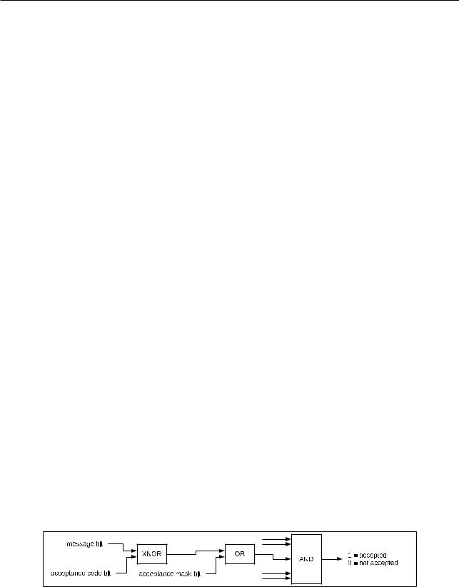
The registers consist of a 32-bit Acceptance Code Value and a 32-bit Acceptance Mask Value. The Code value specifies a bit pattern in which each filtered bit of the message must match in order for the message to be accepted. The Mask value is able to mask out certain bits of the Code value (i.e., set as “Don’t Care” bits). Each filtered bit of the message must either match the acceptance code or be masked in order for the message to be accepted, as demonstrated in Figure 21-7.
The TWAI Controller Acceptance Filter allows the 32-bit Code and Mask values to either define a single filter (i.e., Single Filter Mode), or two filters (i.e., Dual Filter Mode). How the Acceptance Filter interprets the 32-bit code and mask values is dependent on whether Single Filter Mode is enabled, and the received message (i.e., SFF or EFF).
Figure 217. Acceptance Filter
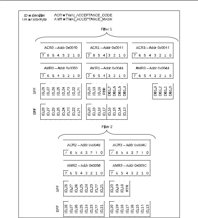
21.5.6.1 Single Filter Mode
Single Filter Mode is enabled by setting the TWAI_RX_FILTER_MODE bit to 1. This will cause the 32-bit code and mask values to define a single filter. The single filter can filter the following bits of a Data or Remote Frame:
• SFF
Espressif Systems |
556 |
ESP32 TRM (Version 5.0) |
Submit Documentation Feedback
21Two-wire Automotive Interface (TWAI)
–The entire 11-bit ID
–RTR bit
–Data byte 1 and Data byte 2
•EFF
–The entire 29-bit ID
–RTR bit
The following Figure 21-8 illustrates how the 32-bit code and mask values will be interpreted under Single Filter Mode.
Figure 218. Single Filter Mode
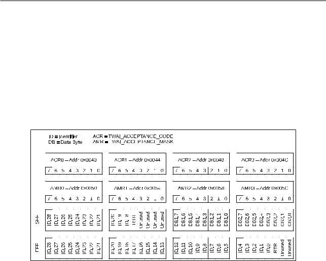
21.5.6.2 Dual FIlter Mode
Dual Filter Mode is enabled by setting the TWAI_RX_FILTER_MODE bit to 0. This will cause the 32-bit code and mask values to define a two separate filters, referred to as filter 1 or two. Under Dual Filter Mode, a message will be accepted if it is accepted by one of the two filters.
The two filters can filter the following bits of a Data or Remote Frame:
•SFF
–The entire 11-bit ID
–RTR bit
–Data byte 1 (for filter 1 only)
•EFF
–The first 16 bits of the 29-bit ID
The following Figure 21-9 illustrates how the 32-bit code and mask values will be interpreted under Dual Filter Mode.
Espressif Systems |
557 |
ESP32 TRM (Version 5.0) |
Submit Documentation Feedback
21 Two-wire Automotive Interface (TWAI)
Figure 219. Dual Filter Mode
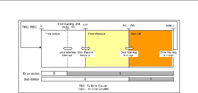
21.5.7 Error Management
The TWAI protocol requires that each TWAI node maintains the Transmit Error Count (TEC) and Receive Error Count (REC). The value of both error counts determine the current error state of the TWAI controller (i.e., Error Active, Error Passive, Bus-Off). The TWAI controller stores the TEC and REC values in the TWAI_TX_ERR_CNT_REG and TWAI_RX_ERR_CNT_REG respectively, and can be read by the CPU at anytime. In addition to the error states, the TWAI controller also offers an Error Warning Limit (EWL) feature that can warn the user regarding the occurrence of severe bus errors before the TWAI controller enters the Error Passive state.
The current error state of the TWAI controller is indicated via a combination of the following values and status bits: TEC, REC, TWAI_ERR_ST, and TWAI_BUS_OFF_ST. Certain changes to these values and bits will also trigger interrupts, thus allowing the users to be notified of error state transitions (see section 21.5.3). The following figure
Espressif Systems |
558 |
ESP32 TRM (Version 5.0) |
Submit Documentation Feedback
21 Two-wire Automotive Interface (TWAI)
21-10 shows the relation between the error states, values and bits, and error state related interrupts.
Figure 2110. Error State Transition
21.5.7.1 Error Warning Limit
The Error Warning Limit (EWL) feature is a configurable threshold value for the TEC and REC, where if exceeded, will trigger an interrupt. The EWL is intended to serve as a warning about severe TWAI bus errors, and is triggered before the TWAI controller enters the Error Passive state. The EWL is configured in the TWAI_ERR_WARNING_LIMIT_REG and can only be configured whilst the TWAI controller is in Reset Mode. The TWAI_ERR_WARNING_LIMIT_REG has a default value of 96. When the values of TEC and/or REC are larger than or equal to the EWL value, the TWAI_ERR_ST bit is immediately set to 1. Likewise, when the values of both the TEC and REC are smaller than the EWL value, the TWAI_ERR_ST bit is immediately reset to 0. The Error Warning Interrupt is triggered whenever the value of the TWAI_ERR_ST bit (or the TWAI_BUS_OFF_ST) changes.
21.5.7.2 Error Passive
The TWAI controller is in the Error Passive state when the TEC or REC value exceeds 127. Likewise, when both the TEC and REC are less than or equal to 127, the TWAI controller enters the Error Active state. The Error Passive Interrupt is triggered whenever the TWAI controller transitions from the Error Active state to the Error Passive state or vice versa.
21.5.7.3 BusOff and BusOff Recovery
The TWAI controller enters the Bus-Off state when the TEC value exceeds 255. On entering the Bus-Off state, the TWAI controller will automatically do the following:
•Set REC to 0
•Set TEC to 127
•Set the TWAI_BUS_OFF_ST bit to 1
•Enter Reset Mode
The Error Warning Interrupt is triggered whenever the value of the TWAI_BUS_OFF_ST bit (or the TWAI_ERR_ST bit) changes.
Espressif Systems |
559 |
ESP32 TRM (Version 5.0) |
Submit Documentation Feedback