

- •1 System and Memory
- •1.1 Introduction
- •1.2 Features
- •1.3 Functional Description
- •1.3.1 Address Mapping
- •1.3.2 Embedded Memory
- •1.3.3 External Memory
- •1.3.5 Peripherals
- •2 Interrupt Matrix (INTERRUPT)
- •2.1 Overview
- •2.2 Features
- •2.3 Functional Description
- •2.3.1 Peripheral Interrupt Source
- •2.3.2 CPU Interrupt
- •2.3.3 Allocate Peripheral Interrupt Sources to Peripheral Interrupt on CPU
- •2.3.4 CPU NMI Interrupt Mask
- •2.3.5 Query Current Interrupt Status of Peripheral Interrupt Source
- •2.4 Registers
- •3 Reset and Clock
- •3.1 System Reset
- •3.1.1 Introduction
- •3.1.2 Reset Source
- •3.2 System Clock
- •3.2.1 Introduction
- •3.2.3 CPU Clock
- •3.2.4 Peripheral Clock
- •3.2.7 Audio PLL
- •3.3 Register Summary
- •3.4 Registers
- •4.1 Overview
- •4.2 Peripheral Input via GPIO Matrix
- •4.2.1 Summary
- •4.2.2 Functional Description
- •4.2.3 Simple GPIO Input
- •4.3 Peripheral Output via GPIO Matrix
- •4.3.1 Summary
- •4.3.3 Simple GPIO Output
- •4.4 Direct I/O via IO_MUX
- •4.4.1 Summary
- •4.4.2 Functional Description
- •4.5 RTC IO_MUX for Low Power and Analog I/O
- •4.5.1 Summary
- •4.5.2 Analog Function Description
- •4.7 Pad Hold Feature
- •4.8 I/O Pad Power Supplies
- •4.8.1 VDD_SDIO Power Domain
- •4.9 Peripheral Signal List
- •4.10 IO_MUX Pad List
- •4.11 RTC_MUX Pin List
- •4.12 Register Summary
- •4.12.1 GPIO Matrix Register Summary
- •4.12.2 IO MUX Register Summary
- •4.12.3 RTC IO MUX Register Summary
- •4.13 Registers
- •4.13.1 GPIO Matrix Registers
- •4.13.2 IO MUX Registers
- •4.13.3 RTC IO MUX Registers
- •5 DPort Registers
- •5.1 Introduction
- •5.2 Features
- •5.3 Functional Description
- •5.3.1 System and Memory Register
- •5.3.2 Reset and Clock Registers
- •5.3.3 Interrupt Matrix Register
- •5.3.4 DMA Registers
- •5.3.5 MPU/MMU Registers
- •5.3.7 Peripheral Clock Gating and Reset
- •5.4 Register Summary
- •5.5 Registers
- •6 DMA Controller (DMA)
- •6.1 Overview
- •6.2 Features
- •6.3 Functional Description
- •6.3.1 DMA Engine Architecture
- •6.3.2 Linked List
- •6.4 UART DMA (UDMA)
- •7 SPI Controller (SPI)
- •7.1 Overview
- •7.5 Parallel QSPI
- •7.5.1 Communication Format of Parallel QSPI
- •7.6.1 SPI Interrupts
- •7.6.2 DMA Interrupts
- •7.7 Register Summary
- •7.8 Registers
- •8 SDIO Slave Controller
- •8.1 Overview
- •8.2 Features
- •8.3 Functional Description
- •8.3.1 SDIO Slave Block Diagram
- •8.3.3 Register Access
- •8.3.6 SDIO Bus Timing
- •8.3.7 Interrupt
- •8.4 Register Summary
- •8.5 SLC Registers
- •8.6 SLC Host Registers
- •8.7 HINF Registers
- •9 SD/MMC Host Controller
- •9.1 Overview
- •9.2 Features
- •9.3 SD/MMC External Interface Signals
- •9.4 Functional Description
- •9.4.1 SD/MMC Host Controller Architecture
- •9.4.2 Command Path
- •9.4.3 Data Path
- •9.5 Software Restrictions for Proper CIU Operation
- •9.6 RAM for Receiving and Sending Data
- •9.6.1 Transmit RAM Module
- •9.6.2 Receive RAM Module
- •9.8 The Structure of a Linked List
- •9.9 Initialization
- •9.9.1 DMAC Initialization
- •9.9.2 DMAC Transmission Initialization
- •9.9.3 DMAC Reception Initialization
- •9.11 Interrupt
- •9.12 Register Summary
- •9.13 Registers
- •10 Ethernet Media Access Controller (MAC)
- •10.1 Overview
- •10.2 EMAC_CORE
- •10.2.1 Transmit Operation
- •10.2.2 Receive Operation
- •10.3 MAC Interrupt Controller
- •10.4 MAC Address Filtering
- •10.4.1 Unicast Destination Address Filtering
- •10.4.2 Multicast Destination Address Filtering
- •10.4.3 Broadcast Address Filtering
- •10.4.4 Unicast Source Address Filtering
- •10.4.5 Inverse Filtering Operation
- •10.4.6 Good Transmitted Frames and Received Frames
- •10.5 EMAC_MTL (MAC Transaction Layer)
- •10.6 PHY Interface
- •10.6.1 MII (Media Independent Interface)
- •10.6.3 Station Management Agent (SMA) Interface
- •10.6.4 RMII Timing
- •10.7 Ethernet DMA Features
- •10.8 Linked List Descriptors
- •10.8.1 Transmit Descriptors
- •10.8.2 Receive Descriptors
- •10.9 Register Summary
- •10.10 Registers
- •11 I2C Controller (I2C)
- •11.1 Overview
- •11.2 Features
- •11.3 Functional Description
- •11.3.1 Introduction
- •11.3.2 Architecture
- •11.3.3 I2C Bus Timing
- •11.3.7 Interrupts
- •11.4 Register Summary
- •11.5 Registers
- •12 I2S Controller (I2S)
- •12.1 Overview
- •12.2 Features
- •12.3 The Clock of I2S Module
- •12.4 I2S Mode
- •12.4.1 Supported Audio Standards
- •12.4.2 Module Reset
- •12.4.3 FIFO Operation
- •12.4.5 Receiving Data
- •12.5.1 LCD Master Transmitting Mode
- •12.5.2 Camera Slave Receiving Mode
- •12.5.3 ADC/DAC mode
- •12.6 I2S Interrupts
- •12.6.1 FIFO Interrupts
- •12.6.2 DMA Interrupts
- •12.7 Register Summary
- •12.8 Registers
- •13 UART Controller (UART)
- •13.1 Overview
- •13.2 UART Features
- •13.3 Functional Description
- •13.3.1 Introduction
- •13.3.3 UART RAM
- •13.3.5 UART Data Frame
- •13.3.7 Flow Control
- •13.3.8 UART DMA
- •13.3.9 UART Interrupts
- •13.3.10 UHCI Interrupts
- •13.4 Register Summary
- •13.4.1 UART Register Summary
- •13.5 Registers
- •13.5.1 UART Registers
- •13.5.2 UHCI Registers
- •14 LED PWM Controller (LEDC)
- •14.1 Introduction
- •14.2 Functional Description
- •14.2.1 Architecture
- •14.2.3 Channels
- •14.2.4 Interrupts
- •14.3 Register Summary
- •14.4 Registers
- •15 Remote Control Peripheral (RMT)
- •15.1 Introduction
- •15.2 Functional Description
- •15.2.1 RMT Architecture
- •15.2.3 Clock
- •15.2.4 Transmitter
- •15.2.5 Receiver
- •15.2.6 Interrupts
- •15.3 Register Summary
- •15.4 Registers
- •16 Motor Control PWM (PWM)
- •16.1 Introduction
- •16.2 Features
- •16.3 Submodules
- •16.3.1 Overview
- •16.3.2 PWM Timer Submodule
- •16.3.3 PWM Operator Submodule
- •16.3.4 Capture Submodule
- •16.4 Register Summary
- •16.5 Registers
- •17 Pulse Count Controller (PCNT)
- •17.1 Overview
- •17.2 Functional Description
- •17.2.1 Architecture
- •17.2.2 Counter Channel Inputs
- •17.2.3 Watchpoints
- •17.2.4 Examples
- •17.2.5 Interrupts
- •18 Timer Group (TIMG)
- •18.1 Introduction
- •18.2 Functional Description
- •18.2.2 64-bit Time-base Counter
- •18.2.3 Alarm Generation
- •18.2.4 MWDT
- •18.2.5 Interrupts
- •18.3 Register Summary
- •18.4 Registers
- •19 Watchdog Timers (WDT)
- •19.1 Introduction
- •19.2 Features
- •19.3 Functional Description
- •19.3.1 Clock
- •20 eFuse Controller
- •20.1 Introduction
- •20.2 Features
- •20.3 Functional Description
- •20.3.1 Structure
- •20.3.3 Software Reading of System Parameters
- •20.3.4 The Use of System Parameters by Hardware Modules
- •20.3.5 Interrupts
- •20.4 Register Summary
- •20.5 Registers
- •21 Two-wire Automotive Interface (TWAI)
- •21.1 Overview
- •21.2 Features
- •21.3 Functional Protocol
- •21.3.1 TWAI Properties
- •21.3.2 TWAI Messages
- •21.3.3 TWAI Errors
- •21.3.4 TWAI Bit Timing
- •21.4 Architectural Overview
- •21.4.1 Registers Block
- •21.4.2 Bit Stream Processor
- •21.4.3 Error Management Logic
- •21.4.4 Bit Timing Logic
- •21.4.5 Acceptance Filter
- •21.5 Functional Description
- •21.5.1 Modes
- •21.5.2 Bit Timing
- •21.5.3 Interrupt Management
- •21.5.4 Transmit and Receive Buffers
- •21.5.5 Receive FIFO and Data Overruns
- •21.5.6 Acceptance Filter
- •21.5.8 Error Code Capture
- •21.5.9 Arbitration Lost Capture
- •21.6 Register Summary
- •21.7 Registers
- •22 AES Accelerator (AES)
- •22.1 Introduction
- •22.2 Features
- •22.3 Functional Description
- •22.3.1 AES Algorithm Operations
- •22.3.2 Key, Plaintext and Ciphertext
- •22.3.3 Endianness
- •22.3.4 Encryption and Decryption Operations
- •22.3.5 Speed
- •22.4 Register Summary
- •22.5 Registers
- •23 SHA Accelerator (SHA)
- •23.1 Introduction
- •23.2 Features
- •23.3 Functional Description
- •23.3.1 Padding and Parsing the Message
- •23.3.2 Message Digest
- •23.3.3 Hash Operation
- •23.3.4 Speed
- •23.4 Register Summary
- •23.5 Registers
- •24 RSA Accelerator (RSA)
- •24.1 Introduction
- •24.2 Features
- •24.3 Functional Description
- •24.3.1 Initialization
- •24.3.2 Large Number Modular Exponentiation
- •24.3.4 Large Number Multiplication
- •24.4 Register Summary
- •24.5 Registers
- •25 Random Number Generator (RNG)
- •25.1 Introduction
- •25.2 Feature
- •25.3 Functional Description
- •25.5 Register Summary
- •25.6 Register
- •26 External Memory Encryption and Decryption (FLASH)
- •26.1 Overview
- •26.2 Features
- •26.3 Functional Description
- •26.3.1 Key Generator
- •26.3.2 Flash Encryption Block
- •26.3.3 Flash Decryption Block
- •26.4 Register Summary
- •26.5 Register
- •27 Memory Management and Protection Units (MMU, MPU)
- •27.1 Introduction
- •27.2 Features
- •27.3 Functional Description
- •27.3.1 PID Controller
- •28 Process ID Controller (PID)
- •28.1 Overview
- •28.2 Features
- •28.3 Functional Description
- •28.3.1 Interrupt Identification
- •28.3.2 Information Recording
- •28.3.3 Proactive Process Switching
- •28.4 Register Summary
- •28.5 Registers
- •29 On-Chip Sensors and Analog Signal Processing
- •29.1 Introduction
- •29.2 Capacitive Touch Sensor
- •29.2.1 Introduction
- •29.2.2 Features
- •29.2.3 Available GPIOs
- •29.2.4 Functional Description
- •29.2.5 Touch FSM
- •29.3.1 Introduction
- •29.3.2 Features
- •29.3.3 Outline of Function
- •29.3.4 RTC SAR ADC Controllers
- •29.3.5 DIG SAR ADC Controllers
- •29.4.1 Introduction
- •29.4.2 Features
- •29.4.4 Cosine Waveform Generator
- •29.5 Register Summary
- •29.5.1 Sensors
- •29.5.2 Advanced Peripheral Bus
- •29.6 Registers
- •29.6.1 Sensors
- •29.6.2 Advanced Peripheral Bus
- •30 ULP Coprocessor (ULP)
- •30.1 Introduction
- •30.2 Features
- •30.4 Instruction Set
- •30.4.2 ST – Store Data in Memory
- •30.4.3 LD – Load Data from Memory
- •30.4.4 JUMP – Jump to an Absolute Address
- •30.4.5 JUMPR – Jump to a Relative Offset (Conditional upon R0)
- •30.4.7 HALT – End the Program
- •30.4.8 WAKE – Wake up the Chip
- •30.4.10 WAIT – Wait for a Number of Cycles
- •30.4.12 I2C_RD/I2C_WR – Read/Write I²C
- •30.4.13 REG_RD – Read from Peripheral Register
- •30.5 ULP Program Execution
- •30.6 RTC_I2C Controller
- •30.6.1 Configuring RTC_I2C
- •30.6.2 Using RTC_I2C
- •30.7 Register Summary
- •30.7.1 SENS_ULP Address Space
- •30.7.2 RTC_I2C Address Space
- •30.8 Registers
- •30.8.1 SENS_ULP Address Space
- •30.8.2 RTC_I2C Address Space
- •31 Low-Power Management (RTC_CNTL)
- •31.1 Introduction
- •31.2 Features
- •31.3 Functional Description
- •31.3.2 Digital Core Voltage Regulator
- •31.3.4 Flash Voltage Regulator
- •31.3.5 Brownout Detector
- •31.3.6 RTC Module
- •31.3.9 Predefined Power Modes
- •31.3.10 Wakeup Source
- •31.3.12 RTC Timer
- •31.3.13 RTC Boot
- •31.4 Register Summary
- •31.5 Registers
- •Glossary
- •Abbreviations for Peripherals
- •Abbreviations for Registers
- •Revision History

21 Two-wire Automotive Interface (TWAI)
21 Twowire Automotive Interface (TWAI)
21.1Overview
The Two-wire Automotive Interface (TWAI®) is a multi-master, multi-cast communication protocol with error detection and signaling and inbuilt message priorities and arbitration.The TWAI protocol is suited for automotive and industrial applications (Please see TWAI Protocol Description).
ESP32 contains a TWAI controller that can be connected to a TWAI bus via an external transceiver. The TWAI controller contains numerous advanced features, and can be utilized in a wide range of use cases such as automotive products, industrial automation controls, building automation etc.
21.2Features
ESP32 TWAI controller supports the following features:
•compatible with ISO 11898-1 protocol (CAN Specification 2.0)
•Supports Standard Frame Format (11-bit ID) and Extended Frame Format (29-bit ID)
•Bit rates:
–from 25 Kbit/s to 1 Mbit/s in chip revision v0.0/v1.0/v1.1
–from 12.5 Kbit/s to 1 Mbit/s in chip revision v3.0/v3.1
•Multiple modes of operation
–Normal
–Listen Only (no influence on bus)
–Self Test (transmissions do not require acknowledgment)
•64-byte Receive FIFO
•Special transmissions
–Single-shot transmissions (does not automatically re-transmit upon error)
–Self Reception (the TWAI controller transmits and receives messages simultaneously)
•Acceptance Filter (supports single and dual filter modes)
•Error detection and handling
–Error counters
–Configurable Error Warning Limit
–Error Code Capture
–Arbitration Lost Capture
21.3Functional Protocol
21.3.1 TWAI Properties
The TWAI protocol connects two or more nodes in a bus network, and allows for nodes to exchange messages in a latency bounded manner. A TWAI bus will has a following properties.
Espressif Systems |
538 |
ESP32 TRM (Version 5.0) |
Submit Documentation Feedback

21 Two-wire Automotive Interface (TWAI)
Single Channel and NonReturntoZero: The bus consists of a single channel to carry bits, thus communication is half-duplex. Synchronization is also derived from this channel, thus extra channels (e.g., clock or enable) are not required. The bit stream of a TWAI message is encoded using the Non-Return-to-Zero (NRZ) method.
Bit Values: The single channel can either be in a Dominant or Recessive state, representing a logical 0 and a logical 1 respectively. A node transmitting a Dominant state will always override a another node transmitting a Recessive state. The physical implementation on the bus is left to the application level to decide (e.g., differential wiring).
BitStuffing: Certain fields of TWAI messages are bit-stuffed. A Transmitter that transmits five consecutive bits of the same value should automatically insert a complementary bit. Likewise, a Receiver that receives five consecutive bits should treat the next bit as a stuff bit. Bit stuffing is applied to the following fields: SOF, Arbitration Field, Control Field, Data Field, and CRC Sequence (see Section 21.3.2 for more details).
Multicast: All nodes receive the same bits as they are connected to the same bus. Data is consistent across all nodes unless there is a bus error (See Section 21.3.3).
Multimaster: Any node can initiate a transmission. If a transmission is already ongoing, a node will wait until the current transmission is over before beginning its own transmission.
MessagePriorities and Arbitration: If two or more nodes simultaneously initiate a transmission, the TWAI protocol ensures that one node will win arbitration of the bus. The Arbitration Field of the message transmitted by each node is used to determine which node will win arbitration.
Error Detection and Signaling: Each node will actively monitor the bus for errors, and signal the detection errors by transmitting an Error Frame.
Fault Confinement: Each node will maintain a set of error counts that are incremented/decremented according to a set of rules. When the error counts surpass a certain threshold, a node will automatically eliminate itself from the network by switching itself off.
Configurable Bit Rate: The bit rate for a single TWAI bus is configurable. However, all nodes within the same bus must operate at the same bit rate.
Transmitters and Receivers: At any point in time, a TWAI node can either be a Transmitter or a Receiver.
•A node originating a message is a Transmitter. The node remains a Transmitter until the bus is idle or until the node loses arbitration. Note that multiple nodes can be Transmitter if they have yet to lose arbitration.
•All nodes that are not Transmitters are Receivers.
21.3.2 TWAI Messages
TWAI nodes use messages to transmit data, and signal errors to other nodes. Messages are split into various frame types, and some frame types will have different frame formats. The TWAI protocol has of the following frame types:
•Data Frames
•Remote Frames
•Error Frames
•Overload Frames
•Interframe Space
Espressif Systems |
539 |
ESP32 TRM (Version 5.0) |
Submit Documentation Feedback
21 Two-wire Automotive Interface (TWAI)
The TWAI protocol has the following frame formats:
•Standard Frame Format (SFF) that consists of a 11-bit identifier
•Extended Frame Format (EFF) that consists of a 29-bit identifier
21.3.2.1 Data Frames and Remote Frames
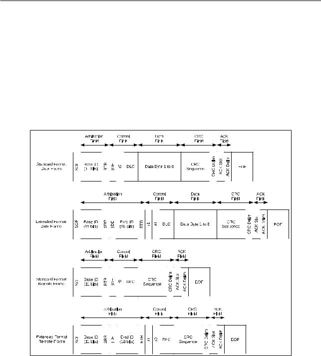
Data Frames are used by nodes to send data to other nodes, and can have a payload of 0 to 8 data bytes. Remote Frames are used to nodes to request a Data Frame with the same Identifier from another node, thus does not contain any data bytes. However, Data Frames and Remote Frames share many common fields. Figure 21-1 illustrates the fields and sub fields of the different frames and formats.
Figure 211. The bit fields of Data Frames and Remote Frames
Arbitration Field
When two or more nodes transmits a Data or Remote Frame simultaneously, the Arbitration Field is used to determine which node will win arbitration of the bus. During the Arbitration Field, if a node transmits a Recessive bit but observes a Dominant bit, this indicates that another node has overridden its Recessive bit. Therefore, the node transmitting the Recessive bit has lost arbitration of the bus and should immediately become a Receiver.
The Arbitration Field primarily consists of the Frame Identifier that is transmitted most significant bit first. Given that a Dominant bit represents a logical 0, and a Recessive bit represents a logical 1:
• A frame with the smallest ID value will always win arbitration.
Espressif Systems |
540 |
ESP32 TRM (Version 5.0) |
Submit Documentation Feedback
21Two-wire Automotive Interface (TWAI)
•Given the same ID and format, Data Frames will always prevail over RTR Frames.
•Given the same first 11 bits of ID, a Standard Format Data Frame will prevail over an Extended Format Data Frame due to the SRR being recessive.
Control Field
The control field primarily consists of the DLC (Data Length Code) which indicates the number of payload data bytes for a Data Frame, or the number of requested data bytes for a Remote Frame. The DLC is transmitted most significant bit first.
Data Field
The Data Field contains the actual payload data bytes of a Data Frame. Remote Frames do not contain a Data Field.
CRC Field
The CRC Field primarily consists of a a CRC Sequence. The CRC Sequence is a 15-bit cyclic redundancy code calculated form the de-stuffed contents (everything from the SOF to the end of the Data Field) of a Data or Remote Frame.
ACK Field
The ACK Field primarily consists of an ACK Slot and an ACK Delim. The ACK Field is mainly intended for the receiver to send a message to a transmitter, indicating it has received an effective message.
Table 211. Data Frames and Remote Frames in SFF and EFF
Data/Remote Frames |
Description |
SOF |
The SOF (Start of Frame) is a single Dominant bit used to synchronize nodes on |
|
the bus. |
|
|
Base ID |
The Base ID (ID.28 to ID.18) is the 11-bit Identifier for SFF, or the first 11-bits of |
|
the 29-bit Identifier for EFF. |
|
|
RTR |
The RTR (Remote Transmission Request) bit indicates whether the message is |
|
a Data Frame (Dominant) or a Remote Frame (Recessive). This means that a |
|
Remote Frame will always lose arbitration to a Data Frame given they have the |
|
same ID. |
|
|
SRR |
The SRR (Substitute Remote Request) bit is transmitted in EFF to substitute for |
|
the RTR bit at the same position in SFF. |
|
|
IDE |
The IDE (Identifier Extension) bit indicates whether the message is SFF (Dominant) |
|
or EFF (Recessive). This means that a SFF frame will always win arbitration over |
|
an EFF frame given they have the same Base ID. |
|
|
Extd ID |
The Extended ID (ID.17 to ID.0) is the remaining 18-bits of the 29-bit identifier for |
|
EFF. |
|
|
r1 |
The r1 (reserved bit 1) is always Dominant. |
|
|
r0 |
The r0 (reserved bit 0) is always Dominant. |
|
|
Espressif Systems |
541 |
ESP32 TRM (Version 5.0) |
Submit Documentation Feedback

21 Two-wire Automotive Interface (TWAI)
Data/Remote Frames |
Description |
DLC |
The DLC (Data Length Code) is 4-bits and should have a value from 0 to 8. |
|
Data Frames use the DLC to indicate the number data bytes in the Data Frame. |
|
Remote Frames used the DLC to indicate the number of data bytes to request |
|
from another node. |
|
|
Data Bytes |
The data payload of Data Frames. The number of bytes should match the value |
|
of DLC. Data byte 0 is transmitted first, and each data byte is transmitted most |
|
significant bit first. |
|
|
CRC Sequence |
The CRC sequence is a 15-bit cyclic redundancy code. |
|
|
CRC Delim |
The CRC Delim (CRC Delimeter) is a single Recessive bit that follows the CRC |
|
sequence. |
|
|
ACK Slot |
The ACK Slot (Acknowledgment Slot) that intended for Receiver nodes to indicate |
|
that the Data or Remote Frame was received without issue. The Transmitter node |
|
will send a Recessive bit in the ACK Slot and Receiver nodes should override the |
|
ACK Slot with a Dominant bit if the frame was received without errors. |
|
|
ACK Delim |
The ACK Delim (Acknowledgment Delimeter) is a single Recessive bit. |
|
|
EOF |
The EOF (End of Frame) marks the end of a Data or Remote Frame, and consists |
|
of seven Recessive bits. |
|
|
21.3.2.2 Error and Overload Frames
Error Frames
Error Frames are transmitted when a node detects a Bus Error. Error Frames notably consist of an Error Flag which is made up of 6 consecutive bits of the same value, thus violating the bit-stuffing rule. Therefore, when a particular node detects a Bus Error and transmits an Error Frame, all other nodes will then detect a Stuff Error and transmit their own Error Frames in response. This has the effect of propagating the detection of a Bus Error across all nodes on the bus. When a node detects a Bus Error, it will transmit an Error Frame starting on the next bit. However, if the type of Bus Error was a CRC Error, then the Error Frame will start at the bit following the ACK Delim (see Section 21.3.3). The following Figure 21-2 shows the various fields of an Error Frame:
|
Figure 212. Various Fields of an Error Frame |
||
|
|
Table 212. Error Frame |
|
|
|
|
|
Error Frame |
|
Description |
|
Error Flag |
|
The Error Flag has two forms, the Active Error Flag consisting of 6 Domi- |
|
|
|
nant bits and the Passive Error Flag consisting of 6 Recessive bits (unless |
|
|
|
overridden by Dominant bits of other nodes). Active Error Flags are sent |
|
|
|
by Error Active nodes, whilst Passive Error Flags are sent by Error Passive |
|
|
|
nodes. |
|
|
|
|
|
Espressif Systems |
542 |
ESP32 TRM (Version 5.0) |
Submit Documentation Feedback
21 Two-wire Automotive Interface (TWAI)
Error Frame |
Description |
Error Flag Superposition |
The Error Flag Superposition field meant to allow for other nodes on the |
|
bus to transmit their respective Active Error Flags. The superposition field |
|
can range from 0 to 6 bits, and ends when the first Recessive bit is de- |
|
tected (i.e., the first it of the Delimeter). |
|
|
Error Delimeter |
The Delimeter field marks the end of the Error/Overload Frame, and con- |
|
sists of 8 Recessive bits. |
|
|
Overload Frames
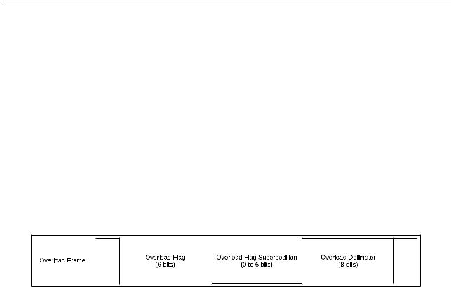
An Overload Frame has the same bit fields as an Error Frame containing an Active Error Flag. The key difference is in the conditions that can trigger the transmission of an Overload Frame. Figure 21-3 below shows the bit fields of an Overload Frame.
Figure 213. The Bit Fields of an Overload Frame
|
Table 213. Overload Frame |
|
|
|
|
Overload Frame |
Description |
|
Overload Flag |
Consists of 6 Dominant bits. Same as an Active Error Flag. |
|
|
|
|
Overload Flag Superposi- |
Allows for the superposition of Overload Flags from other nodes, similar to |
|
tion |
an Error Flag Superposition. |
|
|
|
|
Overload Delimeter |
Consists of 8 Recessive. Same as an Error Delimeter. |
|
|
|
|
Overload Frames will be transmitted under the following conditions:
1.The internal conditions of a Receiver requires a delay of the next Data or Remote Frame.
2.Detection of a Dominant bit at the first and second bit of Intermission.
3.If a Dominant bit is detected at the eighth (last) bit of an Error Delimeter. Note that in this case, TEC and REC will not be incremented (See Section 21.3.3).
Transmitting an overload frame due to one of the conditions must also satisfy the following rules:
•Transmitting an Overload Frame due to condition 1 must only be started at the first bit of Intermission.
•Transmitting an Overload Frame due to condition 2 and 3 must start one bit after the detecting the Dominant bit of the condition.
•A maximum of two Overload frames may be generated in order to delay the next Data or Remote Frame.
Espressif Systems |
543 |
ESP32 TRM (Version 5.0) |
Submit Documentation Feedback