

- •1 System and Memory
- •1.1 Introduction
- •1.2 Features
- •1.3 Functional Description
- •1.3.1 Address Mapping
- •1.3.2 Embedded Memory
- •1.3.3 External Memory
- •1.3.5 Peripherals
- •2 Interrupt Matrix (INTERRUPT)
- •2.1 Overview
- •2.2 Features
- •2.3 Functional Description
- •2.3.1 Peripheral Interrupt Source
- •2.3.2 CPU Interrupt
- •2.3.3 Allocate Peripheral Interrupt Sources to Peripheral Interrupt on CPU
- •2.3.4 CPU NMI Interrupt Mask
- •2.3.5 Query Current Interrupt Status of Peripheral Interrupt Source
- •2.4 Registers
- •3 Reset and Clock
- •3.1 System Reset
- •3.1.1 Introduction
- •3.1.2 Reset Source
- •3.2 System Clock
- •3.2.1 Introduction
- •3.2.3 CPU Clock
- •3.2.4 Peripheral Clock
- •3.2.7 Audio PLL
- •3.3 Register Summary
- •3.4 Registers
- •4.1 Overview
- •4.2 Peripheral Input via GPIO Matrix
- •4.2.1 Summary
- •4.2.2 Functional Description
- •4.2.3 Simple GPIO Input
- •4.3 Peripheral Output via GPIO Matrix
- •4.3.1 Summary
- •4.3.3 Simple GPIO Output
- •4.4 Direct I/O via IO_MUX
- •4.4.1 Summary
- •4.4.2 Functional Description
- •4.5 RTC IO_MUX for Low Power and Analog I/O
- •4.5.1 Summary
- •4.5.2 Analog Function Description
- •4.7 Pad Hold Feature
- •4.8 I/O Pad Power Supplies
- •4.8.1 VDD_SDIO Power Domain
- •4.9 Peripheral Signal List
- •4.10 IO_MUX Pad List
- •4.11 RTC_MUX Pin List
- •4.12 Register Summary
- •4.12.1 GPIO Matrix Register Summary
- •4.12.2 IO MUX Register Summary
- •4.12.3 RTC IO MUX Register Summary
- •4.13 Registers
- •4.13.1 GPIO Matrix Registers
- •4.13.2 IO MUX Registers
- •4.13.3 RTC IO MUX Registers
- •5 DPort Registers
- •5.1 Introduction
- •5.2 Features
- •5.3 Functional Description
- •5.3.1 System and Memory Register
- •5.3.2 Reset and Clock Registers
- •5.3.3 Interrupt Matrix Register
- •5.3.4 DMA Registers
- •5.3.5 MPU/MMU Registers
- •5.3.7 Peripheral Clock Gating and Reset
- •5.4 Register Summary
- •5.5 Registers
- •6 DMA Controller (DMA)
- •6.1 Overview
- •6.2 Features
- •6.3 Functional Description
- •6.3.1 DMA Engine Architecture
- •6.3.2 Linked List
- •6.4 UART DMA (UDMA)
- •7 SPI Controller (SPI)
- •7.1 Overview
- •7.5 Parallel QSPI
- •7.5.1 Communication Format of Parallel QSPI
- •7.6.1 SPI Interrupts
- •7.6.2 DMA Interrupts
- •7.7 Register Summary
- •7.8 Registers
- •8 SDIO Slave Controller
- •8.1 Overview
- •8.2 Features
- •8.3 Functional Description
- •8.3.1 SDIO Slave Block Diagram
- •8.3.3 Register Access
- •8.3.6 SDIO Bus Timing
- •8.3.7 Interrupt
- •8.4 Register Summary
- •8.5 SLC Registers
- •8.6 SLC Host Registers
- •8.7 HINF Registers
- •9 SD/MMC Host Controller
- •9.1 Overview
- •9.2 Features
- •9.3 SD/MMC External Interface Signals
- •9.4 Functional Description
- •9.4.1 SD/MMC Host Controller Architecture
- •9.4.2 Command Path
- •9.4.3 Data Path
- •9.5 Software Restrictions for Proper CIU Operation
- •9.6 RAM for Receiving and Sending Data
- •9.6.1 Transmit RAM Module
- •9.6.2 Receive RAM Module
- •9.8 The Structure of a Linked List
- •9.9 Initialization
- •9.9.1 DMAC Initialization
- •9.9.2 DMAC Transmission Initialization
- •9.9.3 DMAC Reception Initialization
- •9.11 Interrupt
- •9.12 Register Summary
- •9.13 Registers
- •10 Ethernet Media Access Controller (MAC)
- •10.1 Overview
- •10.2 EMAC_CORE
- •10.2.1 Transmit Operation
- •10.2.2 Receive Operation
- •10.3 MAC Interrupt Controller
- •10.4 MAC Address Filtering
- •10.4.1 Unicast Destination Address Filtering
- •10.4.2 Multicast Destination Address Filtering
- •10.4.3 Broadcast Address Filtering
- •10.4.4 Unicast Source Address Filtering
- •10.4.5 Inverse Filtering Operation
- •10.4.6 Good Transmitted Frames and Received Frames
- •10.5 EMAC_MTL (MAC Transaction Layer)
- •10.6 PHY Interface
- •10.6.1 MII (Media Independent Interface)
- •10.6.3 Station Management Agent (SMA) Interface
- •10.6.4 RMII Timing
- •10.7 Ethernet DMA Features
- •10.8 Linked List Descriptors
- •10.8.1 Transmit Descriptors
- •10.8.2 Receive Descriptors
- •10.9 Register Summary
- •10.10 Registers
- •11 I2C Controller (I2C)
- •11.1 Overview
- •11.2 Features
- •11.3 Functional Description
- •11.3.1 Introduction
- •11.3.2 Architecture
- •11.3.3 I2C Bus Timing
- •11.3.7 Interrupts
- •11.4 Register Summary
- •11.5 Registers
- •12 I2S Controller (I2S)
- •12.1 Overview
- •12.2 Features
- •12.3 The Clock of I2S Module
- •12.4 I2S Mode
- •12.4.1 Supported Audio Standards
- •12.4.2 Module Reset
- •12.4.3 FIFO Operation
- •12.4.5 Receiving Data
- •12.5.1 LCD Master Transmitting Mode
- •12.5.2 Camera Slave Receiving Mode
- •12.5.3 ADC/DAC mode
- •12.6 I2S Interrupts
- •12.6.1 FIFO Interrupts
- •12.6.2 DMA Interrupts
- •12.7 Register Summary
- •12.8 Registers
- •13 UART Controller (UART)
- •13.1 Overview
- •13.2 UART Features
- •13.3 Functional Description
- •13.3.1 Introduction
- •13.3.3 UART RAM
- •13.3.5 UART Data Frame
- •13.3.7 Flow Control
- •13.3.8 UART DMA
- •13.3.9 UART Interrupts
- •13.3.10 UHCI Interrupts
- •13.4 Register Summary
- •13.4.1 UART Register Summary
- •13.5 Registers
- •13.5.1 UART Registers
- •13.5.2 UHCI Registers
- •14 LED PWM Controller (LEDC)
- •14.1 Introduction
- •14.2 Functional Description
- •14.2.1 Architecture
- •14.2.3 Channels
- •14.2.4 Interrupts
- •14.3 Register Summary
- •14.4 Registers
- •15 Remote Control Peripheral (RMT)
- •15.1 Introduction
- •15.2 Functional Description
- •15.2.1 RMT Architecture
- •15.2.3 Clock
- •15.2.4 Transmitter
- •15.2.5 Receiver
- •15.2.6 Interrupts
- •15.3 Register Summary
- •15.4 Registers
- •16 Motor Control PWM (PWM)
- •16.1 Introduction
- •16.2 Features
- •16.3 Submodules
- •16.3.1 Overview
- •16.3.2 PWM Timer Submodule
- •16.3.3 PWM Operator Submodule
- •16.3.4 Capture Submodule
- •16.4 Register Summary
- •16.5 Registers
- •17 Pulse Count Controller (PCNT)
- •17.1 Overview
- •17.2 Functional Description
- •17.2.1 Architecture
- •17.2.2 Counter Channel Inputs
- •17.2.3 Watchpoints
- •17.2.4 Examples
- •17.2.5 Interrupts
- •18 Timer Group (TIMG)
- •18.1 Introduction
- •18.2 Functional Description
- •18.2.2 64-bit Time-base Counter
- •18.2.3 Alarm Generation
- •18.2.4 MWDT
- •18.2.5 Interrupts
- •18.3 Register Summary
- •18.4 Registers
- •19 Watchdog Timers (WDT)
- •19.1 Introduction
- •19.2 Features
- •19.3 Functional Description
- •19.3.1 Clock
- •20 eFuse Controller
- •20.1 Introduction
- •20.2 Features
- •20.3 Functional Description
- •20.3.1 Structure
- •20.3.3 Software Reading of System Parameters
- •20.3.4 The Use of System Parameters by Hardware Modules
- •20.3.5 Interrupts
- •20.4 Register Summary
- •20.5 Registers
- •21 Two-wire Automotive Interface (TWAI)
- •21.1 Overview
- •21.2 Features
- •21.3 Functional Protocol
- •21.3.1 TWAI Properties
- •21.3.2 TWAI Messages
- •21.3.3 TWAI Errors
- •21.3.4 TWAI Bit Timing
- •21.4 Architectural Overview
- •21.4.1 Registers Block
- •21.4.2 Bit Stream Processor
- •21.4.3 Error Management Logic
- •21.4.4 Bit Timing Logic
- •21.4.5 Acceptance Filter
- •21.5 Functional Description
- •21.5.1 Modes
- •21.5.2 Bit Timing
- •21.5.3 Interrupt Management
- •21.5.4 Transmit and Receive Buffers
- •21.5.5 Receive FIFO and Data Overruns
- •21.5.6 Acceptance Filter
- •21.5.8 Error Code Capture
- •21.5.9 Arbitration Lost Capture
- •21.6 Register Summary
- •21.7 Registers
- •22 AES Accelerator (AES)
- •22.1 Introduction
- •22.2 Features
- •22.3 Functional Description
- •22.3.1 AES Algorithm Operations
- •22.3.2 Key, Plaintext and Ciphertext
- •22.3.3 Endianness
- •22.3.4 Encryption and Decryption Operations
- •22.3.5 Speed
- •22.4 Register Summary
- •22.5 Registers
- •23 SHA Accelerator (SHA)
- •23.1 Introduction
- •23.2 Features
- •23.3 Functional Description
- •23.3.1 Padding and Parsing the Message
- •23.3.2 Message Digest
- •23.3.3 Hash Operation
- •23.3.4 Speed
- •23.4 Register Summary
- •23.5 Registers
- •24 RSA Accelerator (RSA)
- •24.1 Introduction
- •24.2 Features
- •24.3 Functional Description
- •24.3.1 Initialization
- •24.3.2 Large Number Modular Exponentiation
- •24.3.4 Large Number Multiplication
- •24.4 Register Summary
- •24.5 Registers
- •25 Random Number Generator (RNG)
- •25.1 Introduction
- •25.2 Feature
- •25.3 Functional Description
- •25.5 Register Summary
- •25.6 Register
- •26 External Memory Encryption and Decryption (FLASH)
- •26.1 Overview
- •26.2 Features
- •26.3 Functional Description
- •26.3.1 Key Generator
- •26.3.2 Flash Encryption Block
- •26.3.3 Flash Decryption Block
- •26.4 Register Summary
- •26.5 Register
- •27 Memory Management and Protection Units (MMU, MPU)
- •27.1 Introduction
- •27.2 Features
- •27.3 Functional Description
- •27.3.1 PID Controller
- •28 Process ID Controller (PID)
- •28.1 Overview
- •28.2 Features
- •28.3 Functional Description
- •28.3.1 Interrupt Identification
- •28.3.2 Information Recording
- •28.3.3 Proactive Process Switching
- •28.4 Register Summary
- •28.5 Registers
- •29 On-Chip Sensors and Analog Signal Processing
- •29.1 Introduction
- •29.2 Capacitive Touch Sensor
- •29.2.1 Introduction
- •29.2.2 Features
- •29.2.3 Available GPIOs
- •29.2.4 Functional Description
- •29.2.5 Touch FSM
- •29.3.1 Introduction
- •29.3.2 Features
- •29.3.3 Outline of Function
- •29.3.4 RTC SAR ADC Controllers
- •29.3.5 DIG SAR ADC Controllers
- •29.4.1 Introduction
- •29.4.2 Features
- •29.4.4 Cosine Waveform Generator
- •29.5 Register Summary
- •29.5.1 Sensors
- •29.5.2 Advanced Peripheral Bus
- •29.6 Registers
- •29.6.1 Sensors
- •29.6.2 Advanced Peripheral Bus
- •30 ULP Coprocessor (ULP)
- •30.1 Introduction
- •30.2 Features
- •30.4 Instruction Set
- •30.4.2 ST – Store Data in Memory
- •30.4.3 LD – Load Data from Memory
- •30.4.4 JUMP – Jump to an Absolute Address
- •30.4.5 JUMPR – Jump to a Relative Offset (Conditional upon R0)
- •30.4.7 HALT – End the Program
- •30.4.8 WAKE – Wake up the Chip
- •30.4.10 WAIT – Wait for a Number of Cycles
- •30.4.12 I2C_RD/I2C_WR – Read/Write I²C
- •30.4.13 REG_RD – Read from Peripheral Register
- •30.5 ULP Program Execution
- •30.6 RTC_I2C Controller
- •30.6.1 Configuring RTC_I2C
- •30.6.2 Using RTC_I2C
- •30.7 Register Summary
- •30.7.1 SENS_ULP Address Space
- •30.7.2 RTC_I2C Address Space
- •30.8 Registers
- •30.8.1 SENS_ULP Address Space
- •30.8.2 RTC_I2C Address Space
- •31 Low-Power Management (RTC_CNTL)
- •31.1 Introduction
- •31.2 Features
- •31.3 Functional Description
- •31.3.2 Digital Core Voltage Regulator
- •31.3.4 Flash Voltage Regulator
- •31.3.5 Brownout Detector
- •31.3.6 RTC Module
- •31.3.9 Predefined Power Modes
- •31.3.10 Wakeup Source
- •31.3.12 RTC Timer
- •31.3.13 RTC Boot
- •31.4 Register Summary
- •31.5 Registers
- •Glossary
- •Abbreviations for Peripherals
- •Abbreviations for Registers
- •Revision History

16 Motor Control PWM (PWM)
16.3.2.3 PWM Timer Shadow Register
The PWM timer’s period register and the PWM timer’s clock prescaler register have shadow registers. The purpose of a shadow register is to save a copy of the value to be written into the active register at a specific moment synchronized with the hardware. Both register types are defined as follows:
•Active Register
This register is directly responsible for controlling all actions performed by hardware.
•Shadow Register
It acts as a temporary buffer for a value to be written on the active register. Before this happens, the content of the shadow register has no direct effect on the controlled hardware. At a specific, user-configured point in time, the value saved in the shadow register is copied to the active register. This helps to prevent spurious operation of the hardware, which may happen when a register is asynchronously modified by software. Both the shadow register and the active register have the same memory address. The software always writes into, or reads from the shadow register. The moment of updating the active register is determined by its specific update method register. The update can start when the PWM timer is equal to zero, when the PWM timer is equal to period,at a synchronization moment, or immediately. Software can trigger a globally forced update which will prompt all registers in the module to be updated according to shadow registers.
16.3.2.4 PWM Timer Synchronization and Phase Locking
The PWM modules adopt a flexible synchronization method. Each PWM timer has a synchronization input and a synchronization output. The synchronization input can be selected from three synchronization outputs and three synchronization signals from the GPIO matrix. The synchronization output can be generated from the synchronization input signal, or when the PWM timer’s value is equal to period or zero. Thus, the PWM timers can be chained together with their phase locked. During synchronization, the PWM timer clock prescaler will reset its counter in order to synchronize the PWM timer clock.
16.3.3 PWM Operator Submodule
The PWM Operator submodule has the following functions:
•Generates a PWM signal pair, based on timing references obtained from the corresponding PWM timer.
•Each signal out of the PWM signal pair includes a specific pattern of dead time.
•Superimposes a carrier on the PWM signal, if configured to do so.
•Handles response under fault conditions.
Figure 16-14 shows the block diagram of a PWM operator.
Espressif Systems |
420 |
ESP32 TRM (Version 5.0) |
Submit Documentation Feedback
16 Motor Control PWM (PWM)
Figure 1614. Submodules Inside the PWM Operator
Espressif Systems |
421 |
ESP32 TRM (Version 5.0) |
Submit Documentation Feedback

16 Motor Control PWM (PWM)
16.3.3.1 PWM Generator Submodule
Purpose of the PWM Generator Submodule
In this submodule, important timing events are generated or imported. The events are then converted into specific actions to generate the desired waveforms at the PWMxA and PWMxB outputs.
The PWM generator submodule performs the following actions:
•Generation of timing events based on time stamps configured using the A and B registers. Events happen when the following conditions are satisfied:
–UTEA: the PWM timer is counting up and its value is equal to register A.
–UTEB: the PWM timer is counting up and its value is equal to register B.
–DTEA: the PWM timer is counting down and its value is equal to register A.
–DTEB: the PWM timer is counting down and its value is equal to register B.
•Generation of U/DT1, U/DT2 timing events based on fault or synchronization events.
•Management of priority when these timing events occur concurrently.
•Qualification and generation of set, clear and toggle actions, based on the timing events.
•Controlling of the PWM duty cycle, depending on configuration of the PWM generator submodule.
•Handling of new time stamp values, using shadow, registers to prevent glitches in the PWM cycle.
PWM Operator Shadow Registers
The time stamp registers A and B, as well as action configuration registers PWM_GENx_A_REG and PWM_GENx_B_REG are shadowed. Shadowing provides a way of updating registers in sync with the hardware. For a description of
the shadow registers, please see 16.3.2.3.
Timing Events
For convenience, all timing signals and events are summarized in Table 16-2.
Table 162. Timing Events Used in PWM Generator
|
Signal |
Event Description |
PWM Timer Operation |
|
DTEP |
PWM timer value is equal to the period register value |
|
|
|
|
|
|
DTEZ |
PWM timer value is equal to zero |
|
|
|
|
|
|
DTEA |
PWM timer value is equal to A register |
PWM timer counts down. |
|
|
|
|
|
DTEB |
PWM timer value is equal to B register |
|
|
|
||
|
|
|
|
|
DT0 event |
Based on fault or synchronization events |
|
|
|
|
|
|
DT1 event |
Based on fault or synchronization events |
|
|
|
|
|
|
UTEP |
PWM timer value is equal to the period register value |
|
|
|
|
|
|
UTEZ |
PWM timer value is equal to zero |
|
|
|
|
|
|
UTEA |
PWM timer value is equal to A register |
PWM timer counts up. |
|
|
|
|
|
UTEB |
PWM timer value is equal to B register |
|
|
|
||
|
|
|
|
|
UT0 event |
Based on fault or synchronization events |
|
|
|
|
|
|
UT1 event |
Based on fault or synchronization events |
|
|
|
|
|
Espressif Systems |
422 |
ESP32 TRM (Version 5.0) |
|
Submit Documentation Feedback

16 Motor Control PWM (PWM)
Signal |
Event Description |
PWM Timer Operation |
Software-force event |
Software-initiated asynchronous event |
N/A |
|
|
|
The purpose of a software-force event is to impose non-continuous or continuous changes on the PWMxA and PWMxB outputs. The change is done asynchronously. Software-force control is handled by the PWM_PWM_GENx_FORCE_REG registers.
The selection and configuration of T0/T1 in the PWM generator submodule is independent of the configuration of fault events in the fault handler submodule. A particular trip event may or may not be configured to cause trip action in the fault handler submodule, but the same event can be used by the PWM generator to trigger T0/T1 for controlling PWM waveforms.
It is important to know that when the PWM timer is in count-up-down mode, it will always decrement after a TEP event, and will always increment after a TEZ event. So when the PWM timer is in count-up-down mode, DTEP and UTEZ events will occur, while the events UTEP and DTEZ will never occur.
The PWM generator can handle multiple events at the same time. Events are prioritized by the hardware and relevant details are provided in Table 16-3 and Table 16-4. Priority levels range from 1 (the highest) to 7 (the lowest). Please note that the priority of TEP and TEZ events depends on the PWM timer’s direction.
If the value of A or B is set to be greater than the period, then U/DTEA and U/DTEB will never occur.
Table 163. Timing Events Priority When PWM Timer Increments
Priority Level |
Event |
|
1 |
(highest) |
Software-force event |
|
|
|
2 |
|
UTEP |
|
|
|
3 |
|
UT0 |
|
|
|
4 |
|
UT1 |
|
|
|
5 |
|
UTEB |
|
|
|
6 |
|
UTEA |
|
|
|
7 |
(lowest) |
UTEZ |
|
|
|
|
Table 164. Timing Events Priority when PWM Timer Decrements |
|
|
|
|
Priority level |
Event |
|
1 |
(highest) |
Software-force event |
|
|
|
2 |
|
DTEZ |
|
|
|
3 |
|
DT0 |
|
|
|
4 |
|
DT1 |
|
|
|
5 |
|
DTEB |
|
|
|
6 |
|
DTEA |
|
|
|
7 |
(lowest) |
DTEP |
|
|
|
Notes:
1.UTEP and UTEZ do not happen simultaneously. When the PWM timer is in count-up mode, UTEP will always happen one cycle earlier than UTEZ, as demonstrated in Figure 16-11, so their action on PWM signals will
Espressif Systems |
423 |
ESP32 TRM (Version 5.0) |
Submit Documentation Feedback

16 Motor Control PWM (PWM)
not interrupt each other. When the PWM timer is in count-up-down mode, UTEP will not occur.
2.DTEP and DTEZ do not happen simultaneously. When the PWM timer is in count-down mode, DTEZ will always happen one cycle earlier than DTEP, as demonstrated in Figure 16-12, so their action on PWM signals will not interrupt each other. When the PWM timer is in count-up-down mode, DTEZ will not occur.
PWM Signal Generation
The PWM generator submodule controls the behavior of outputs PWMxA and PWMxB when a particular timing event occurs. The timing events are further qualified by the PWM timer’s counting direction (up or down). Knowing the counting direction, the submodule may then perform an independent action at each stage of the PWM timer counting up or down.
The following actions may be configured on outputs PWMxA and PWMxB:
•Set High:
Set the output of PWMxA or PWMxB to a high level.
•Clear Low:
Clear the output of PWMxA or PWMxB by setting it to a low level.
•Toggle:
Change the current output level of PWMxA or PWMxB to the opposite value. If it is currently pulled high, pull it low, or vice versa.
•Do Nothing:
Keep both outputs PWMxA and PWMxB unchanged. In this state, interrupts can still be triggered.
The configuration of actions on outputs is done by using registers PWN_GENx_A_REG and PWN_GENx_B_REG. So, the action to be taken on each output is set independently. Also there is great flexibility in selecting actions to be taken on a given output based on events. More specifically, any event listed in Table 16-2 can operate on either output PWMxA or PWMxB. To check out registers for particular generator 0, 1 or 2, please refer to register description in Section 16.4.
Waveforms for Common Configurations
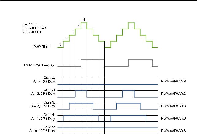
Figure 16-15 presents the symmetric PWM waveform generated when the PWM timer is counting up and down. DC 0%–100% modulation can be calculated via the formula below:
Duty = (P eriod − A) ÷ P eriod
If A matches the PWM timer value and the PWM timer is incrementing, then the PWM output is pulled up. If A matches the PWM timer value while the PWM timer is decrementing, then the PWM output is pulled low.
Espressif Systems |
424 |
ESP32 TRM (Version 5.0) |
Submit Documentation Feedback
16 Motor Control PWM (PWM)
Figure 1615. Symmetrical Waveform in CountUpDown Mode
The PWM waveforms in Figures 16-16 to 16-19 show some common PWM operator configurations. The following conventions are used in the figures:
•Period A and B refer to the values written in the corresponding registers.
•PWMxA and PWMxB are the output signals of PWM Operator x.
Espressif Systems |
425 |
ESP32 TRM (Version 5.0) |
Submit Documentation Feedback
16 Motor Control PWM (PWM)
Figure 1616. CountUp, Single Edge Asymmetric Waveform, with Independent Modulation on PWMxA and PWMxB — Active High
The duty modulation for PWMxA is set by B, active high and proportional to B.
The duty modulation for PWMxB is set by A, active high and proportional to A.
P eriod = (P W M_T IMERx_P ERIOD + 1) × TPT_clk
Espressif Systems |
426 |
ESP32 TRM (Version 5.0) |
Submit Documentation Feedback

16 Motor Control PWM (PWM)
Figure 1617. CountUp, Pulse Placement Asymmetric Waveform with Independent Modulation on PWMxA
Pulses may be generated anywhere within the PWM cycle (zero – period).
PWMxA’s high time duty is proportional to (B – A).
P eriod = (P W M_T IMERx_P ERIOD + 1) × TPT_clk
Espressif Systems |
427 |
ESP32 TRM (Version 5.0) |
Submit Documentation Feedback
16 Motor Control PWM (PWM)
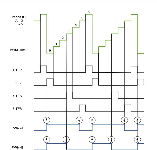
Figure 1618. CountUpDown, Dual Edge Symmetric Waveform, with Independent Modulation on PWMxA and PWMxB — Active High
The duty modulation for PWMxA is set by A, active high and proportional to A.
The duty modulation for PWMxB is set by B, active high and proportional to B.
Outputs PWMxA and PWMxB can drive independent switches.
P eriod = (2 × P W M_T IMERx_P ERIOD + 1) × TPT_clk
Espressif Systems |
428 |
ESP32 TRM (Version 5.0) |
Submit Documentation Feedback
16 Motor Control PWM (PWM)
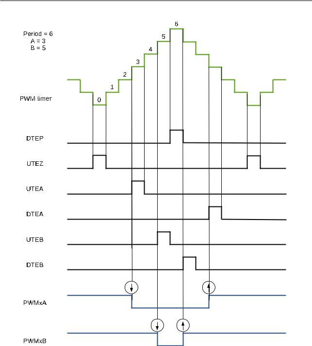
Figure 1619. CountUpDown, Dual Edge Symmetric Waveform, with Independent Modulation on PWMxA and PWMxB — Complementary
The duty modulation of PWMxA is set by A, is active high and proportional to A.
The duty modulation of PWMxB is set by B, is active low and proportional to B.
Outputs PWMx can drive upper/lower (complementary) switches.
Dead-time = B – A; Edge placement is fully programmable by software. Use the dead-time generator module if another edge delay method is required.
P eriod = (2 × P W M_T IMERx_P ERIOD + 1) × TPT_clk
Espressif Systems |
429 |
ESP32 TRM (Version 5.0) |
Submit Documentation Feedback
16 Motor Control PWM (PWM)
SoftwareForce Events
There are two types of software-force events inside the PWM generator:
•Non-continuous-immediate (NCI) software-force events
Such types of events are immediately effective on PWM outputs when triggered by software. The forcing is non-continuous, meaning the next active timing events will be able to alter the PWM outputs.
•Continuous (CNTU) software-force events
Such types of events are continuous. The forced PWM outputs will continue until they are released by software. The events’ triggers are configurable. They can be timing events or immediate events.
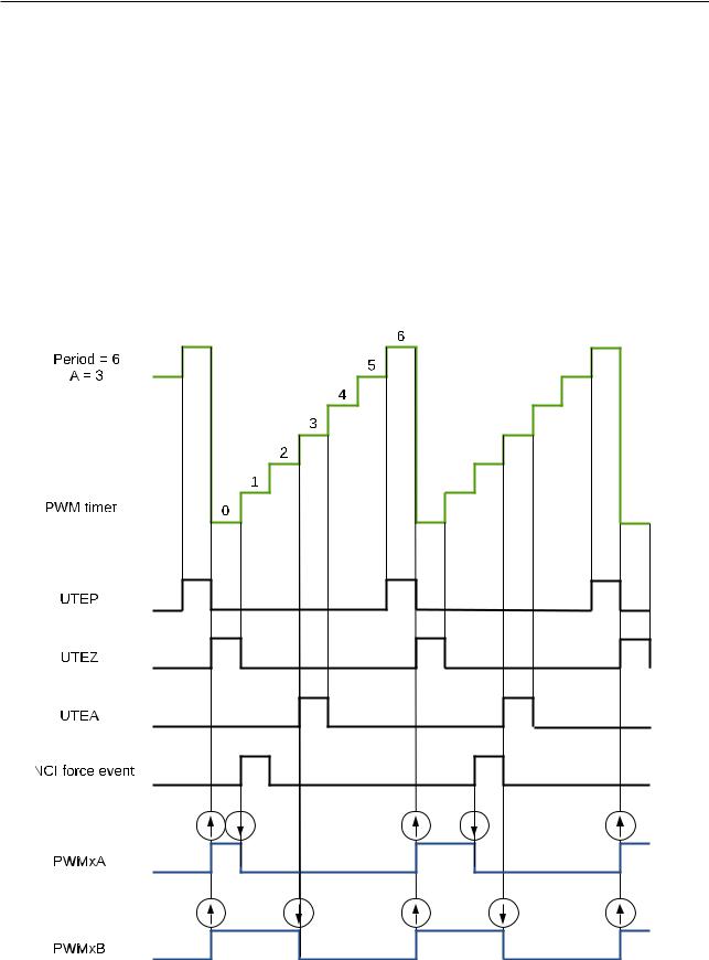
Figure 16-20 shows a waveform of NCI software-force events. NCI events are used to force PWMxA output low. Forcing on PWMxB is disabled in this case.
Figure 1620. Example of an NCI SoftwareForce Event on PWMxA
Espressif Systems |
430 |
ESP32 TRM (Version 5.0) |
Submit Documentation Feedback
16 Motor Control PWM (PWM)
Figure 16-21 shows a waveform of CNTU software-force events. UTEZ events are selected as triggers for CNTU software-force events. CNTU is used to force the PWMxB output low. Forcing on PWMxA is disabled.
Figure 1621. Example of a CNTU SoftwareForce Event on PWMxB
Espressif Systems |
431 |
ESP32 TRM (Version 5.0) |
Submit Documentation Feedback

16 Motor Control PWM (PWM)
16.3.3.2 Dead Time Generator Submodule
Purpose of the Dead Time Generator Submodule
Several options to generate signals on PWMxA and PWMxB outputs, with a specific placement of signal edges, have been discussed in section 16.3.3.1. The required dead time is obtained by altering the edge placement between signals and by setting the signal’s duty cycle. Another option is to control the dead time using a specialized submodule – the Dead Time Generator.
The key functions of the dead time generator submodule are as follows:
•Generating signal pairs (PWMxA and PWMxB) with a dead time from a single PWMxA input
•Creating a dead time by adding delay to signal edges:
–Rising edge delay (RED)
–Falling edge delay (FED)
•Configuring the signal pairs to be:
–Active high complementary (AHC)
–Active low complementary (ALC)
–Active high (AH)
–Active low (AL)
•This submodule may also be bypassed, if the dead time is configured directly in the generator submodule.
Dead Time Generator’s Shadow Registers
Delay registers RED and FED are shadowed with registers PWM_DTx_RED_CFG_REG and PWM_DTx_FED_CFG_REG. For the description of shadow registers, please see section 16.3.2.3.
Espressif Systems |
432 |
ESP32 TRM (Version 5.0) |
Submit Documentation Feedback
16 Motor Control PWM (PWM)
Highlights for Operation of the Dead Time Generator
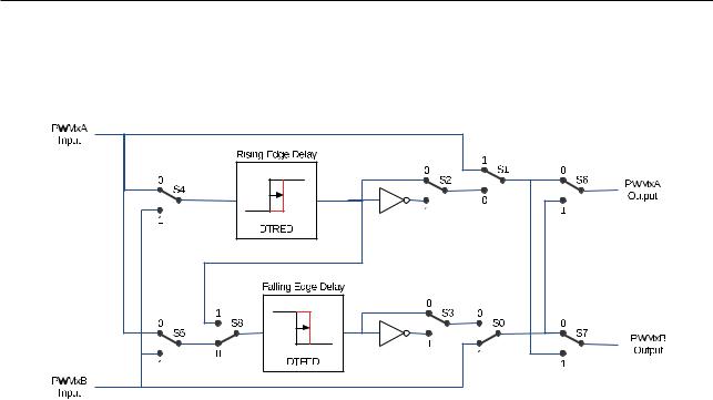
Options for setting up the dead-time submodule are shown in Figure 16-22.
Figure 1622. Options for Setting up the Dead Time Generator Submodule
S0-8 in the figure above are switches controlled by registers PWM_DTx_CFG_REG shown in Table 16-5.
Table 165. Dead Time Generator Switches Control Registers
Switch |
Register |
S0 |
PWM_DTx_B_OUTBYPASS |
|
|
S1 |
PWM_DTx_A_OUTBYPASS |
|
|
S2 |
PWM_DTx_RED_OUTINVERT |
|
|
S3 |
PWM_DTx_FED_OUTINVERT |
|
|
S4 |
PWM_DTx_RED_INSEL |
|
|
S5 |
PWM_DTx_FED_INSEL |
|
|
S6 |
PWM_DTx_A_OUTSWAP |
|
|
S7 |
PWM_DTx_B_OUTSWAP |
|
|
S8 |
PWM_DTx_DEB_MODE |
|
|
All switch combinations are supported, but not all of them represent the typical modes of use. Table 16-6 documents some typical dead time configurations. In these configurations the position of S4 and S5 sets PWMxA as the common source of both falling-edge and rising-edge delay. The modes presented in table 16-6 may be categorized as follows:
•Mode 1: Bypass delays on both falling (FED) as well as raising edge (RED)
In this mode the dead time submodule is disabled. Signals PWMxA and PWMxB pass through without any modifications.
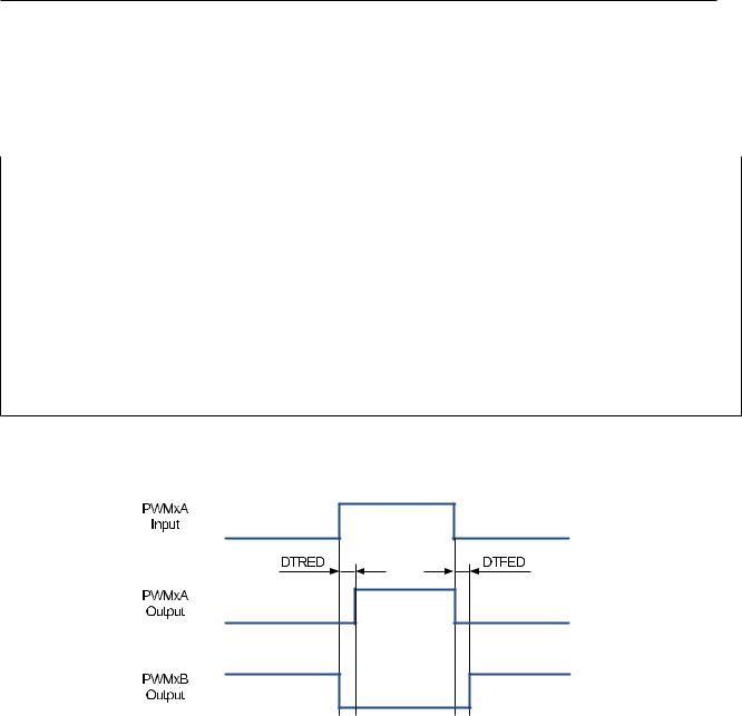
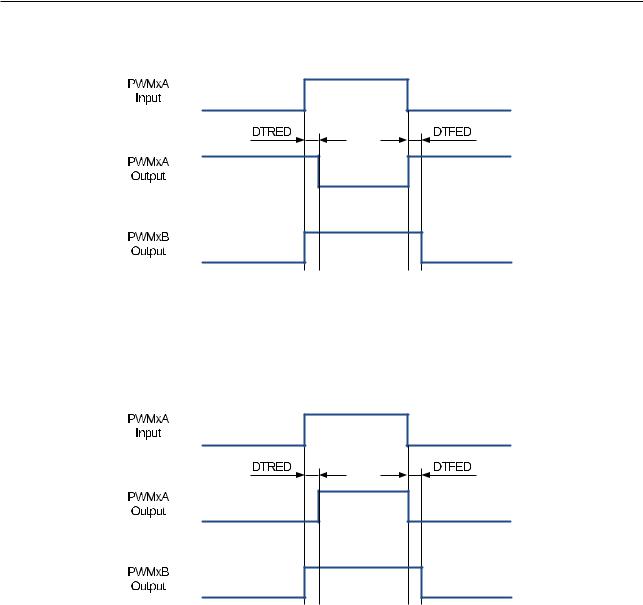
•Mode 25: Classical Dead Time Polarity Settings
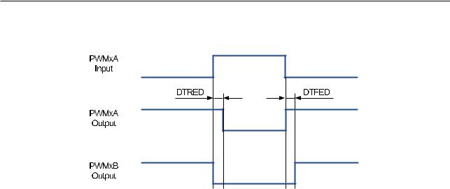
These modes represent typical configurations of polarity and should cover the active-high/low modes in available industry power switch gate drivers. The typical waveforms are shown in Figures 16-23 to 16-26.
Espressif Systems |
433 |
ESP32 TRM (Version 5.0) |
Submit Documentation Feedback
16 Motor Control PWM (PWM)
•Modes 6 and 7: Bypass delay on falling edge (FED) or rising edge (RED)
In these modes, either RED (Rising Edge Delay) or FED (Falling Edge Delay) is bypassed. As a result, the corresponding delay is not applied.
Table 166. Typical Dead Time Generator Operating Modes
Mode |
Mode Description |
S0 |
S1 |
S2 |
S3 |
1 |
PWMxA and PWMxB Pass Through/No Delay |
1 |
1 |
X |
X |
|
|
|
|
|
|
2 |
Active High Complementary (AHC), see Figure 16-23 |
0 |
0 |
0 |
1 |
|
|
|
|
|
|
3 |
Active Low Complementary (ALC), see Figure 16-24 |
0 |
0 |
1 |
0 |
|
|
|
|
|
|
4 |
Active High (AH), see Figure 16-25 |
0 |
0 |
0 |
0 |
|
|
|
|
|
|
5 |
Active Low (AL), see Figure 16-26 |
0 |
0 |
1 |
1 |
|
|
|
|
|
|
6 |
PWMxA Output = PWMxA In (No Delay) |
0 |
1 |
0 or 1 |
0 or 1 |
|
PWMxB Output = PWMxA Input with Falling Edge Delay |
|
|
|
|
|
|
|
|
|
|
7 |
PWMxA Output = PWMxA Input with Rising Edge Delay |
1 |
0 |
0 or 1 |
0 or 1 |
|
PWMxB Output = PWMxB Input with No Delay |
|
|
|
|
|
|
|
|
|
|
Note: For all the modes above, the position of the binary switches S4 to S8 is set to 0.
Figure 1623. Active High Complementary (AHC) Dead Time Waveforms
Espressif Systems |
434 |
ESP32 TRM (Version 5.0) |
Submit Documentation Feedback
16 Motor Control PWM (PWM)
Figure 1624. Active Low Complementary (ALC) Dead Time Waveforms
Figure 1625. Active High (AH) Dead Time Waveforms
Espressif Systems |
435 |
ESP32 TRM (Version 5.0) |
Submit Documentation Feedback
16 Motor Control PWM (PWM)
Figure 1626. Active Low (AL) Dead Time Waveforms
Rising edge (RED) and falling edge (FED) delays may be set up independently. The delay value is programmed using the 16-bit registers PWM_DTx_RED and PWM_DTx_FED. The register value represents the number of clock (DT_clk) periods by which a signal edge is delayed. DT_CLK can be selected from PWM_clk or PT_clk through register PWM_DTx_CLK_SEL.
To calculate the delay on falling edge (FED) and rising edge (RED), use the following formulas:
F ED = P W M_DT x_F ED × TDT_clk
RED = P W M_DT x_RED × TDT_clk
Espressif Systems |
436 |
ESP32 TRM (Version 5.0) |
Submit Documentation Feedback

16 Motor Control PWM (PWM)
16.3.3.3 PWM Carrier Submodule
The coupling of PWM output to a motor driver may need isolation with a transformer. Transformers deliver only AC signals, while the duty cycle of a PWM signal may range anywhere from 0% to 100%. The PWM carrier submodule passes such a PWM signal through a transformer by using a high frequency carrier to modulate the signal.
Function Overview
The following key characteristics of this submodule are configurable:
•Carrier frequency
•Pulse width of the first pulse
•Duty cycle of the second and the subsequent pulses
•Enabling/disabling the carrier function
Operational Highlights
The PWM carrier clock (PC_clk) is derived from PWM_clk. The frequency and duty cycle are configured by the PWM_CARRIERx_PRESCALE and PWM_CARRIERx_DUTY bits in the PWM_CARRIERx_CFG_REG register. The purpose of one-shot pulses is to provide high-energy impulse to reliably turn on the power switch. Subsequent pulses sustain the power-on status. The width of a one-shot pulse is configurable with the PWM_CARRIERx_OSHTWTH bits. Enabling/disabling of the carrier submodule is done with the PWM_CARRIERx_EN bit.
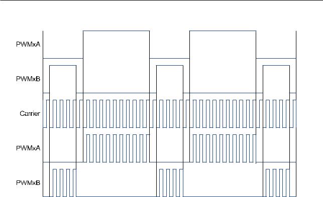
Waveform Examples
Figure 16-27 shows an example of waveforms, where a carrier is superimposed on original PWM pulses. This figure do not show the first one-shot pulse and the duty-cycle control. Related details are covered in the following two sections.
Espressif Systems |
437 |
ESP32 TRM (Version 5.0) |
Submit Documentation Feedback
16 Motor Control PWM (PWM)
Figure 1627. Example of Waveforms Showing PWM Carrier Action
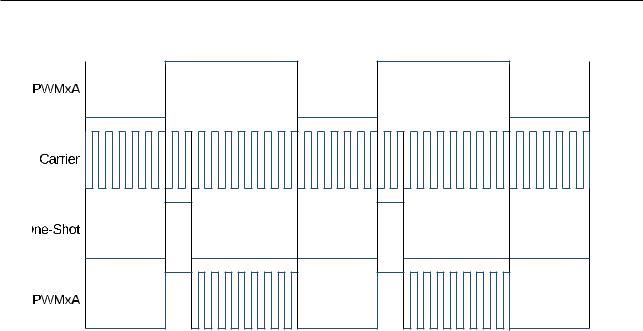
OneShot Pulse
The width of the first pulse is configurable. It may assume one of 16 possible values and is described by the formula below:
T1stpulse = TPWM_clk ×8 ×(P W M_CARRIERx_P RESCALE + 1) ×(P W M_CARRIERx_OSHT W T H + 1)
Where:
• TPMW_clk is the period of the PWM clock (PWM_clk).
• (P W M_CARRIERx_OSHT W T H + 1) is the width of the first pulse (whose value ranges from 1 to 16).
• (P W M_CARRIERx_P RESCALE + 1) is the PWM carrier clock’s (PC_clk) prescaler value. The first one-shot pulse and subsequent sustaining pulses are shown in Figure 16-28.
Espressif Systems |
438 |
ESP32 TRM (Version 5.0) |
Submit Documentation Feedback
16 Motor Control PWM (PWM)
Figure 1628. Example of the First Pulse and the Subsequent Sustaining Pulses of the PWM Carrier Sub module
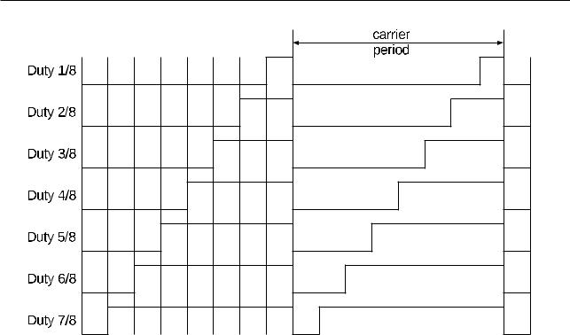
Duty Cycle Control
After issuing the first one-shot pulse, the remaining PWM signal is modulated according to the carrier frequency. Users can configure the duty cycle of this signal. Tuning of duty may be required, so that the signal passes through the isolating transformer and can still operate (turn on/off) the motor drive, changing rotation speed and direction.
The duty cycle may be set to one of seven values, using PWM_CARRIERx_DUTY, or bits [7:5] of register PWM_CARRIERx_CFG_REG.
Below is the formula for calculating the duty cycle:
Duty = P W M_CARRIERx_DUT Y ÷ 8
All seven settings of the duty cycle are shown in Figure 16-29.
Espressif Systems |
439 |
ESP32 TRM (Version 5.0) |
Submit Documentation Feedback
16 Motor Control PWM (PWM)
Figure 1629. Possible Duty Cycle Settings for Sustaining Pulses in the PWM Carrier Submodule
16.3.3.4 Fault Handler Submodule
Each MCPWM peripheral is connected to three fault signals (FAULT0, FAULT1 and FAULT2) which are sourced from the GPIO matrix. These signals are intended to indicate external fault conditions, and may be preprocessed by the fault detection submodule to generate fault events. Fault events can then execute the user code to control MCPWM outputs in response to specific faults.
Function of Fault Handler Submodule
The key actions performed by the fault handler submodule are:
•Forcing outputs PWMxA and PWMxB, upon detected fault, to one of the following states:
–High
–Low
–Toggle
–No action taken
•Execution of one-shot trip (OST) upon detection of over-current conditions/short circuits.
•Cycle-by-cycle tripping (CBC) to provide current-limiting operation.
•Allocation of either one-shot or cycle-by-cycle operation for each fault signal.
•Generation of interrupts for each fault input.
•Support for software-force tripping.
•Enabling or disabling of submodule function as required.
Espressif Systems |
440 |
ESP32 TRM (Version 5.0) |
Submit Documentation Feedback