

- •1 System and Memory
- •1.1 Introduction
- •1.2 Features
- •1.3 Functional Description
- •1.3.1 Address Mapping
- •1.3.2 Embedded Memory
- •1.3.3 External Memory
- •1.3.5 Peripherals
- •2 Interrupt Matrix (INTERRUPT)
- •2.1 Overview
- •2.2 Features
- •2.3 Functional Description
- •2.3.1 Peripheral Interrupt Source
- •2.3.2 CPU Interrupt
- •2.3.3 Allocate Peripheral Interrupt Sources to Peripheral Interrupt on CPU
- •2.3.4 CPU NMI Interrupt Mask
- •2.3.5 Query Current Interrupt Status of Peripheral Interrupt Source
- •2.4 Registers
- •3 Reset and Clock
- •3.1 System Reset
- •3.1.1 Introduction
- •3.1.2 Reset Source
- •3.2 System Clock
- •3.2.1 Introduction
- •3.2.3 CPU Clock
- •3.2.4 Peripheral Clock
- •3.2.7 Audio PLL
- •3.3 Register Summary
- •3.4 Registers
- •4.1 Overview
- •4.2 Peripheral Input via GPIO Matrix
- •4.2.1 Summary
- •4.2.2 Functional Description
- •4.2.3 Simple GPIO Input
- •4.3 Peripheral Output via GPIO Matrix
- •4.3.1 Summary
- •4.3.3 Simple GPIO Output
- •4.4 Direct I/O via IO_MUX
- •4.4.1 Summary
- •4.4.2 Functional Description
- •4.5 RTC IO_MUX for Low Power and Analog I/O
- •4.5.1 Summary
- •4.5.2 Analog Function Description
- •4.7 Pad Hold Feature
- •4.8 I/O Pad Power Supplies
- •4.8.1 VDD_SDIO Power Domain
- •4.9 Peripheral Signal List
- •4.10 IO_MUX Pad List
- •4.11 RTC_MUX Pin List
- •4.12 Register Summary
- •4.12.1 GPIO Matrix Register Summary
- •4.12.2 IO MUX Register Summary
- •4.12.3 RTC IO MUX Register Summary
- •4.13 Registers
- •4.13.1 GPIO Matrix Registers
- •4.13.2 IO MUX Registers
- •4.13.3 RTC IO MUX Registers
- •5 DPort Registers
- •5.1 Introduction
- •5.2 Features
- •5.3 Functional Description
- •5.3.1 System and Memory Register
- •5.3.2 Reset and Clock Registers
- •5.3.3 Interrupt Matrix Register
- •5.3.4 DMA Registers
- •5.3.5 MPU/MMU Registers
- •5.3.7 Peripheral Clock Gating and Reset
- •5.4 Register Summary
- •5.5 Registers
- •6 DMA Controller (DMA)
- •6.1 Overview
- •6.2 Features
- •6.3 Functional Description
- •6.3.1 DMA Engine Architecture
- •6.3.2 Linked List
- •6.4 UART DMA (UDMA)
- •7 SPI Controller (SPI)
- •7.1 Overview
- •7.5 Parallel QSPI
- •7.5.1 Communication Format of Parallel QSPI
- •7.6.1 SPI Interrupts
- •7.6.2 DMA Interrupts
- •7.7 Register Summary
- •7.8 Registers
- •8 SDIO Slave Controller
- •8.1 Overview
- •8.2 Features
- •8.3 Functional Description
- •8.3.1 SDIO Slave Block Diagram
- •8.3.3 Register Access
- •8.3.6 SDIO Bus Timing
- •8.3.7 Interrupt
- •8.4 Register Summary
- •8.5 SLC Registers
- •8.6 SLC Host Registers
- •8.7 HINF Registers
- •9 SD/MMC Host Controller
- •9.1 Overview
- •9.2 Features
- •9.3 SD/MMC External Interface Signals
- •9.4 Functional Description
- •9.4.1 SD/MMC Host Controller Architecture
- •9.4.2 Command Path
- •9.4.3 Data Path
- •9.5 Software Restrictions for Proper CIU Operation
- •9.6 RAM for Receiving and Sending Data
- •9.6.1 Transmit RAM Module
- •9.6.2 Receive RAM Module
- •9.8 The Structure of a Linked List
- •9.9 Initialization
- •9.9.1 DMAC Initialization
- •9.9.2 DMAC Transmission Initialization
- •9.9.3 DMAC Reception Initialization
- •9.11 Interrupt
- •9.12 Register Summary
- •9.13 Registers
- •10 Ethernet Media Access Controller (MAC)
- •10.1 Overview
- •10.2 EMAC_CORE
- •10.2.1 Transmit Operation
- •10.2.2 Receive Operation
- •10.3 MAC Interrupt Controller
- •10.4 MAC Address Filtering
- •10.4.1 Unicast Destination Address Filtering
- •10.4.2 Multicast Destination Address Filtering
- •10.4.3 Broadcast Address Filtering
- •10.4.4 Unicast Source Address Filtering
- •10.4.5 Inverse Filtering Operation
- •10.4.6 Good Transmitted Frames and Received Frames
- •10.5 EMAC_MTL (MAC Transaction Layer)
- •10.6 PHY Interface
- •10.6.1 MII (Media Independent Interface)
- •10.6.3 Station Management Agent (SMA) Interface
- •10.6.4 RMII Timing
- •10.7 Ethernet DMA Features
- •10.8 Linked List Descriptors
- •10.8.1 Transmit Descriptors
- •10.8.2 Receive Descriptors
- •10.9 Register Summary
- •10.10 Registers
- •11 I2C Controller (I2C)
- •11.1 Overview
- •11.2 Features
- •11.3 Functional Description
- •11.3.1 Introduction
- •11.3.2 Architecture
- •11.3.3 I2C Bus Timing
- •11.3.7 Interrupts
- •11.4 Register Summary
- •11.5 Registers
- •12 I2S Controller (I2S)
- •12.1 Overview
- •12.2 Features
- •12.3 The Clock of I2S Module
- •12.4 I2S Mode
- •12.4.1 Supported Audio Standards
- •12.4.2 Module Reset
- •12.4.3 FIFO Operation
- •12.4.5 Receiving Data
- •12.5.1 LCD Master Transmitting Mode
- •12.5.2 Camera Slave Receiving Mode
- •12.5.3 ADC/DAC mode
- •12.6 I2S Interrupts
- •12.6.1 FIFO Interrupts
- •12.6.2 DMA Interrupts
- •12.7 Register Summary
- •12.8 Registers
- •13 UART Controller (UART)
- •13.1 Overview
- •13.2 UART Features
- •13.3 Functional Description
- •13.3.1 Introduction
- •13.3.3 UART RAM
- •13.3.5 UART Data Frame
- •13.3.7 Flow Control
- •13.3.8 UART DMA
- •13.3.9 UART Interrupts
- •13.3.10 UHCI Interrupts
- •13.4 Register Summary
- •13.4.1 UART Register Summary
- •13.5 Registers
- •13.5.1 UART Registers
- •13.5.2 UHCI Registers
- •14 LED PWM Controller (LEDC)
- •14.1 Introduction
- •14.2 Functional Description
- •14.2.1 Architecture
- •14.2.3 Channels
- •14.2.4 Interrupts
- •14.3 Register Summary
- •14.4 Registers
- •15 Remote Control Peripheral (RMT)
- •15.1 Introduction
- •15.2 Functional Description
- •15.2.1 RMT Architecture
- •15.2.3 Clock
- •15.2.4 Transmitter
- •15.2.5 Receiver
- •15.2.6 Interrupts
- •15.3 Register Summary
- •15.4 Registers
- •16 Motor Control PWM (PWM)
- •16.1 Introduction
- •16.2 Features
- •16.3 Submodules
- •16.3.1 Overview
- •16.3.2 PWM Timer Submodule
- •16.3.3 PWM Operator Submodule
- •16.3.4 Capture Submodule
- •16.4 Register Summary
- •16.5 Registers
- •17 Pulse Count Controller (PCNT)
- •17.1 Overview
- •17.2 Functional Description
- •17.2.1 Architecture
- •17.2.2 Counter Channel Inputs
- •17.2.3 Watchpoints
- •17.2.4 Examples
- •17.2.5 Interrupts
- •18 Timer Group (TIMG)
- •18.1 Introduction
- •18.2 Functional Description
- •18.2.2 64-bit Time-base Counter
- •18.2.3 Alarm Generation
- •18.2.4 MWDT
- •18.2.5 Interrupts
- •18.3 Register Summary
- •18.4 Registers
- •19 Watchdog Timers (WDT)
- •19.1 Introduction
- •19.2 Features
- •19.3 Functional Description
- •19.3.1 Clock
- •20 eFuse Controller
- •20.1 Introduction
- •20.2 Features
- •20.3 Functional Description
- •20.3.1 Structure
- •20.3.3 Software Reading of System Parameters
- •20.3.4 The Use of System Parameters by Hardware Modules
- •20.3.5 Interrupts
- •20.4 Register Summary
- •20.5 Registers
- •21 Two-wire Automotive Interface (TWAI)
- •21.1 Overview
- •21.2 Features
- •21.3 Functional Protocol
- •21.3.1 TWAI Properties
- •21.3.2 TWAI Messages
- •21.3.3 TWAI Errors
- •21.3.4 TWAI Bit Timing
- •21.4 Architectural Overview
- •21.4.1 Registers Block
- •21.4.2 Bit Stream Processor
- •21.4.3 Error Management Logic
- •21.4.4 Bit Timing Logic
- •21.4.5 Acceptance Filter
- •21.5 Functional Description
- •21.5.1 Modes
- •21.5.2 Bit Timing
- •21.5.3 Interrupt Management
- •21.5.4 Transmit and Receive Buffers
- •21.5.5 Receive FIFO and Data Overruns
- •21.5.6 Acceptance Filter
- •21.5.8 Error Code Capture
- •21.5.9 Arbitration Lost Capture
- •21.6 Register Summary
- •21.7 Registers
- •22 AES Accelerator (AES)
- •22.1 Introduction
- •22.2 Features
- •22.3 Functional Description
- •22.3.1 AES Algorithm Operations
- •22.3.2 Key, Plaintext and Ciphertext
- •22.3.3 Endianness
- •22.3.4 Encryption and Decryption Operations
- •22.3.5 Speed
- •22.4 Register Summary
- •22.5 Registers
- •23 SHA Accelerator (SHA)
- •23.1 Introduction
- •23.2 Features
- •23.3 Functional Description
- •23.3.1 Padding and Parsing the Message
- •23.3.2 Message Digest
- •23.3.3 Hash Operation
- •23.3.4 Speed
- •23.4 Register Summary
- •23.5 Registers
- •24 RSA Accelerator (RSA)
- •24.1 Introduction
- •24.2 Features
- •24.3 Functional Description
- •24.3.1 Initialization
- •24.3.2 Large Number Modular Exponentiation
- •24.3.4 Large Number Multiplication
- •24.4 Register Summary
- •24.5 Registers
- •25 Random Number Generator (RNG)
- •25.1 Introduction
- •25.2 Feature
- •25.3 Functional Description
- •25.5 Register Summary
- •25.6 Register
- •26 External Memory Encryption and Decryption (FLASH)
- •26.1 Overview
- •26.2 Features
- •26.3 Functional Description
- •26.3.1 Key Generator
- •26.3.2 Flash Encryption Block
- •26.3.3 Flash Decryption Block
- •26.4 Register Summary
- •26.5 Register
- •27 Memory Management and Protection Units (MMU, MPU)
- •27.1 Introduction
- •27.2 Features
- •27.3 Functional Description
- •27.3.1 PID Controller
- •28 Process ID Controller (PID)
- •28.1 Overview
- •28.2 Features
- •28.3 Functional Description
- •28.3.1 Interrupt Identification
- •28.3.2 Information Recording
- •28.3.3 Proactive Process Switching
- •28.4 Register Summary
- •28.5 Registers
- •29 On-Chip Sensors and Analog Signal Processing
- •29.1 Introduction
- •29.2 Capacitive Touch Sensor
- •29.2.1 Introduction
- •29.2.2 Features
- •29.2.3 Available GPIOs
- •29.2.4 Functional Description
- •29.2.5 Touch FSM
- •29.3.1 Introduction
- •29.3.2 Features
- •29.3.3 Outline of Function
- •29.3.4 RTC SAR ADC Controllers
- •29.3.5 DIG SAR ADC Controllers
- •29.4.1 Introduction
- •29.4.2 Features
- •29.4.4 Cosine Waveform Generator
- •29.5 Register Summary
- •29.5.1 Sensors
- •29.5.2 Advanced Peripheral Bus
- •29.6 Registers
- •29.6.1 Sensors
- •29.6.2 Advanced Peripheral Bus
- •30 ULP Coprocessor (ULP)
- •30.1 Introduction
- •30.2 Features
- •30.4 Instruction Set
- •30.4.2 ST – Store Data in Memory
- •30.4.3 LD – Load Data from Memory
- •30.4.4 JUMP – Jump to an Absolute Address
- •30.4.5 JUMPR – Jump to a Relative Offset (Conditional upon R0)
- •30.4.7 HALT – End the Program
- •30.4.8 WAKE – Wake up the Chip
- •30.4.10 WAIT – Wait for a Number of Cycles
- •30.4.12 I2C_RD/I2C_WR – Read/Write I²C
- •30.4.13 REG_RD – Read from Peripheral Register
- •30.5 ULP Program Execution
- •30.6 RTC_I2C Controller
- •30.6.1 Configuring RTC_I2C
- •30.6.2 Using RTC_I2C
- •30.7 Register Summary
- •30.7.1 SENS_ULP Address Space
- •30.7.2 RTC_I2C Address Space
- •30.8 Registers
- •30.8.1 SENS_ULP Address Space
- •30.8.2 RTC_I2C Address Space
- •31 Low-Power Management (RTC_CNTL)
- •31.1 Introduction
- •31.2 Features
- •31.3 Functional Description
- •31.3.2 Digital Core Voltage Regulator
- •31.3.4 Flash Voltage Regulator
- •31.3.5 Brownout Detector
- •31.3.6 RTC Module
- •31.3.9 Predefined Power Modes
- •31.3.10 Wakeup Source
- •31.3.12 RTC Timer
- •31.3.13 RTC Boot
- •31.4 Register Summary
- •31.5 Registers
- •Glossary
- •Abbreviations for Peripherals
- •Abbreviations for Registers
- •Revision History
16 Motor Control PWM (PWM)
16.3Submodules
16.3.1 Overview
This section lists the configuration parameters of key submodules. For information on adjusting a specific parameter, e.g. synchronization source of PWM timer, please refer to Section 16.3.2 for details.
16.3.1.1 Prescaler Submodule
Figure 162. Prescaler Submodule
Configuration parameter:
• Scale the PWM clock according to CLK_160M.
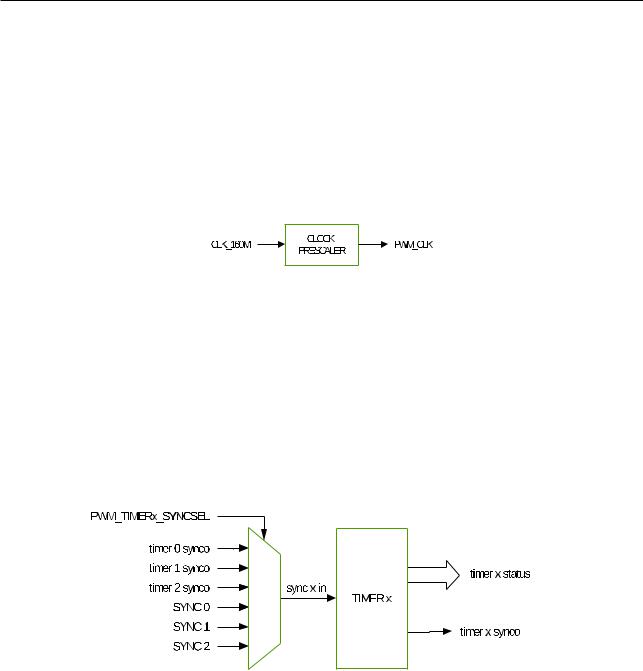
16.3.1.2 Timer Submodule
Figure 163. Timer Submodule
Configuration parameters:
•Set the PWM timer frequency or period.
•Configure the working mode for the timer:
–Count-Up Mode: for asymmetric PWM outputs
–Count-Down Mode: for asymmetric PWM outputs
–Count-Up-Down Mode: for symmetric PWM outputs
•Configure the the reloading phase (including the value and the phase) used during software and hardware synchronization.
Espressif Systems |
412 |
ESP32 TRM (Version 5.0) |
Submit Documentation Feedback
16Motor Control PWM (PWM)
•Synchronize the PWM timers with each other. Either hardware or software synchronization may be used.
•Configure the source of the PWM timer’s the synchronization input to one of the seven sources below:
–The three PWM timer’s synchronization outputs.
–Three synchronization signals from the GPIO matrix: SYNC0, SYNC1, SYNC2.
–No synchronization input signal selected
•Configure the source of the PWM timer’s synchronization output to one of the four sources below:
–Synchronization input signal
–Event generated when value of the PWM timer is equal to zero
–Event generated when value of the PWM timer is equal to period
–No synchronization output generated
•Configure the method of period updating.
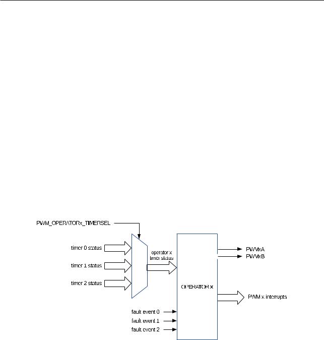
16.3.1.3 Operator Submodule
Figure 164. Operator Submodule
The configuration parameters of the operator submodule are shown in Table 16-1.
Espressif Systems |
413 |
ESP32 TRM (Version 5.0) |
Submit Documentation Feedback

16 Motor Control PWM (PWM)
|
Table 161. Configuration Parameters of the Operator Submodule |
||||
|
|
|
|
||
|
Submodule |
Configuration Parameter or Option |
|
||
|
|
• Set up the PWM duty cycle for PWMxA and/or PWMxB out- |
|
||
|
|
|
put. |
|
|
|
|
• Set up at which time the timing events occur. |
|
||
|
|
• Define what action should be taken on timing events: |
|
||
|
|
|
– Switch high or low PWMxA and/or PWMxB outputs |
|
|
|
PWM Generator |
|
– Toggle PWMxA and/or PWMxB outputs |
|
|
|
|
|
– Take no action on outputs |
|
|
|
|
• Use direct s/w control to force the state of PWM outputs |
|
||
|
|
• Add a dead time to raising and / or failing edge on PWM out- |
|
||
|
|
|
puts. |
|
|
|
|
• Configure update method for this submodule. |
|
||
|
|
|
|
||
|
|
• Control of complementary dead time relationship between |
|
||
|
|
|
upper and lower switches. |
|
|
|
|
• Specify the dead time on rising edge. |
|
||
|
|
• |
Specify the dead time on falling edge. |
|
|
|
Dead Time Generator |
• Bypass the dead time generator module. The PWM wave- |
|
||
|
|
|
form will pass through without inserting dead time. |
|
|
|
|
• Allow PWMxB phase shifting with respect to the PWMxA out- |
|
||
|
|
|
put. |
|
|
|
|
• Configure updating method for this submodule. |
|
||
|
|
|
|
|
|
|
|
• |
Enable carrier and set up carrier frequency. |
|
|
|
|
• |
Configure duration of the first pulse in the carrier waveform. |
|
|
|
PWM Carrier |
• Set up the duty cycle of the following pulses. |
|
||
|
|
• Bypass the PWM carrier module. The PWM waveform will be |
|
||
|
|
|
passed through without modification. |
|
|
|
|
|
|
||
|
|
• Configure if and how the PWM module should react the fault |
|
||
|
|
|
event signals. |
|
|
|
|
• Specify the action taken when a fault event occurs: |
|
||
|
|
|
– Force PWMxA and/or PWMxB high. |
|
|
|
|
|
– Force PWMxA and/or PWMxB low. |
|
|
|
|
|
– Configure PWMxA and/or PWMxB to ignore any fault |
|
|
|
|
|
event. |
|
|
|
Fault Handler |
• Configure how often the PWM should react to fault events: |
|
||
|
|
|
– One-shot |
|
|
|
|
|
– Cycle-by-cycle |
|
|
|
|
• |
Generate interrupts. |
|
|
|
|
• |
Bypass the fault handler submodule entirely. |
|
|
|
|
• |
Set up an option for cycle-by-cycle actions clearing. |
|
|
|
|
• If desired, |
independently-configured actions can be taken |
|
|
|
|
|
when time-base counter is counting down or up. |
|
|
|
|
|
|
|
|
Espressif Systems |
|
414 |
ESP32 TRM (Version 5.0) |
||
Submit Documentation Feedback
16 Motor Control PWM (PWM)
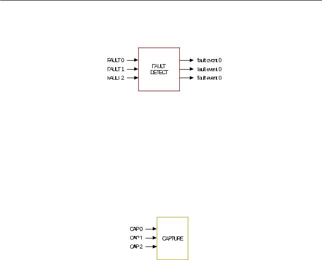
16.3.1.4 Fault Detection Submodule
Figure 165. Fault Detection Submodule
Configuration parameters:
•Enable fault event generation and configure the polarity of fault event generation for every fault signal
•Generate fault event interrupts
16.3.1.5 Capture Submodule
Figure 166. Capture Submodule
Configuration parameters:
•Select the edge polarity and prescaling of the capture input.
•Set up a software-triggered capture.
•Configure the capture timer’s sync trigger and sync phase.
•Software syncs the capture timer.
16.3.2 PWM Timer Submodule
Each MCPWM module has three PWM timer submodules. Any of them can determine the necessary event timing for any of the three PWM operator submodules. Built-in synchronization logic allows multiple PWM timer submodules, in one or more MCPWM modules, to work together as a system, when using synchronization signals from the GPIO matrix.
16.3.2.1 Configurations of the PWM Timer Submodule
Users can configure the following functions of the PWM timer submodule:
•Control how often events occur by specifying the PWM timer frequency or period.
•Configure a particular PWM timer to synchronize with other PWM timers or modules.
Espressif Systems |
415 |
ESP32 TRM (Version 5.0) |
Submit Documentation Feedback
16Motor Control PWM (PWM)
•Get a PWM timer in phase with other PWM timers or modules.
•Set one of the following timer counting modes: count-up, count-down, count-up-down.
•Change the rate of the PWM timer clock (PT_clk) with a prescaler. Each timer has its own prescaler configured with PWM_TIMERx_PRESCALE of register PWM_TIMER0_CFG0_REG. The PWM timer increments or decrements at a slower pace, depending on the setting of this register.
16.3.2.2 PWM Timer’s Working Modes and Timing Event Generation
The PWM timer has three working modes, selected by the PWMx timer mode register:
•Count-Up Mode:
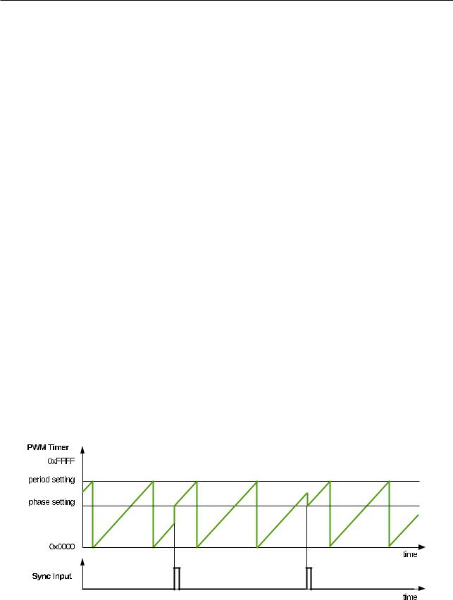
In this mode, the PWM timer increments from zero until reaching the value configured in the period register. Once done, the PWM timer returns to zero and starts increasing again. PWM period is equal to the value of period register + 1.
Note: The period register is PWM_TIMERx_PERIOD (x = 0, 1, 2), i.e., PWM_TIMER0_PERIOD, PWM_TIMER1_PERIOD, PWM_TIMER2_PERIOD.
•Count-Down Mode:
The PWM timer decrements to zero, starting from the value configured in the period register. After reaching zero, it is set back to the period value. Then it starts to decrement again. In this case, the PWM period is also equal to the value of period register + 1.
•Count-Up-Down Mode:
This is a combination of the two modes mentioned above. The PWM timer starts increasing from zero until the period value is reached. Then, the timer decreases back to zero. This pattern is then repeated. The PWM period is the result of (the value of period register × 2 + 1).
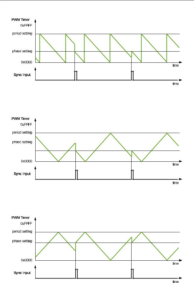
Figures 16-7 to 16-10 show PWM timer waveforms in different modes, including timer behavior during synchronization events.
Figure 167. CountUp Mode Waveform
Espressif Systems |
416 |
ESP32 TRM (Version 5.0) |
Submit Documentation Feedback
16 Motor Control PWM (PWM)
Figure 168. CountDown Mode Waveforms
Figure 169. CountUpDown Mode Waveforms, CountDown at Synchronization Event
Figure 1610. CountUpDown Mode Waveforms, CountUp at Synchronization Event
Espressif Systems 417 ESP32 TRM (Version 5.0)
Submit Documentation Feedback
16 Motor Control PWM (PWM)
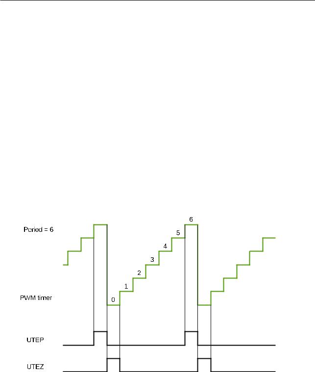
When the PWM timer is running, it generates the following timing events periodically and automatically:
•UTEP
The timing event generated when the PWM timer’s value equals to the value of the period register (PWM_TIMERx_PERIOD) and when the PWM timer is increasing.
•UTEZ
The timing event generated when the PWM timer’s value equals to zero and when the PWM timer is increasing.
•DTEP
The timing event generated when the PWM timer’s value equals to the value of the period register (PWM_TIMERx_PERIOD) and when the PWM timer is decreasing.
•DTEZ
The timing event generated when the PWM timer’s value equals to zero and when the PWM timer is decreasing.
Figures 16-11 to 16-13 show the timing waveforms of U/DTEP and U/DTEZ.
Figure 1611. UTEP and UTEZ Generation in CountUp Mode
Espressif Systems |
418 |
ESP32 TRM (Version 5.0) |
Submit Documentation Feedback

16 Motor Control PWM (PWM)
Figure 1612. DTEP and DTEZ Generation in CountDown Mode
|
Figure 1613. DTEP and UTEZ Generation in CountUpDown Mode |
|
Espressif Systems |
419 |
ESP32 TRM (Version 5.0) |
Submit Documentation Feedback