

- •1 System and Memory
- •1.1 Introduction
- •1.2 Features
- •1.3 Functional Description
- •1.3.1 Address Mapping
- •1.3.2 Embedded Memory
- •1.3.3 External Memory
- •1.3.5 Peripherals
- •2 Interrupt Matrix (INTERRUPT)
- •2.1 Overview
- •2.2 Features
- •2.3 Functional Description
- •2.3.1 Peripheral Interrupt Source
- •2.3.2 CPU Interrupt
- •2.3.3 Allocate Peripheral Interrupt Sources to Peripheral Interrupt on CPU
- •2.3.4 CPU NMI Interrupt Mask
- •2.3.5 Query Current Interrupt Status of Peripheral Interrupt Source
- •2.4 Registers
- •3 Reset and Clock
- •3.1 System Reset
- •3.1.1 Introduction
- •3.1.2 Reset Source
- •3.2 System Clock
- •3.2.1 Introduction
- •3.2.3 CPU Clock
- •3.2.4 Peripheral Clock
- •3.2.7 Audio PLL
- •3.3 Register Summary
- •3.4 Registers
- •4.1 Overview
- •4.2 Peripheral Input via GPIO Matrix
- •4.2.1 Summary
- •4.2.2 Functional Description
- •4.2.3 Simple GPIO Input
- •4.3 Peripheral Output via GPIO Matrix
- •4.3.1 Summary
- •4.3.3 Simple GPIO Output
- •4.4 Direct I/O via IO_MUX
- •4.4.1 Summary
- •4.4.2 Functional Description
- •4.5 RTC IO_MUX for Low Power and Analog I/O
- •4.5.1 Summary
- •4.5.2 Analog Function Description
- •4.7 Pad Hold Feature
- •4.8 I/O Pad Power Supplies
- •4.8.1 VDD_SDIO Power Domain
- •4.9 Peripheral Signal List
- •4.10 IO_MUX Pad List
- •4.11 RTC_MUX Pin List
- •4.12 Register Summary
- •4.12.1 GPIO Matrix Register Summary
- •4.12.2 IO MUX Register Summary
- •4.12.3 RTC IO MUX Register Summary
- •4.13 Registers
- •4.13.1 GPIO Matrix Registers
- •4.13.2 IO MUX Registers
- •4.13.3 RTC IO MUX Registers
- •5 DPort Registers
- •5.1 Introduction
- •5.2 Features
- •5.3 Functional Description
- •5.3.1 System and Memory Register
- •5.3.2 Reset and Clock Registers
- •5.3.3 Interrupt Matrix Register
- •5.3.4 DMA Registers
- •5.3.5 MPU/MMU Registers
- •5.3.7 Peripheral Clock Gating and Reset
- •5.4 Register Summary
- •5.5 Registers
- •6 DMA Controller (DMA)
- •6.1 Overview
- •6.2 Features
- •6.3 Functional Description
- •6.3.1 DMA Engine Architecture
- •6.3.2 Linked List
- •6.4 UART DMA (UDMA)
- •7 SPI Controller (SPI)
- •7.1 Overview
- •7.5 Parallel QSPI
- •7.5.1 Communication Format of Parallel QSPI
- •7.6.1 SPI Interrupts
- •7.6.2 DMA Interrupts
- •7.7 Register Summary
- •7.8 Registers
- •8 SDIO Slave Controller
- •8.1 Overview
- •8.2 Features
- •8.3 Functional Description
- •8.3.1 SDIO Slave Block Diagram
- •8.3.3 Register Access
- •8.3.6 SDIO Bus Timing
- •8.3.7 Interrupt
- •8.4 Register Summary
- •8.5 SLC Registers
- •8.6 SLC Host Registers
- •8.7 HINF Registers
- •9 SD/MMC Host Controller
- •9.1 Overview
- •9.2 Features
- •9.3 SD/MMC External Interface Signals
- •9.4 Functional Description
- •9.4.1 SD/MMC Host Controller Architecture
- •9.4.2 Command Path
- •9.4.3 Data Path
- •9.5 Software Restrictions for Proper CIU Operation
- •9.6 RAM for Receiving and Sending Data
- •9.6.1 Transmit RAM Module
- •9.6.2 Receive RAM Module
- •9.8 The Structure of a Linked List
- •9.9 Initialization
- •9.9.1 DMAC Initialization
- •9.9.2 DMAC Transmission Initialization
- •9.9.3 DMAC Reception Initialization
- •9.11 Interrupt
- •9.12 Register Summary
- •9.13 Registers
- •10 Ethernet Media Access Controller (MAC)
- •10.1 Overview
- •10.2 EMAC_CORE
- •10.2.1 Transmit Operation
- •10.2.2 Receive Operation
- •10.3 MAC Interrupt Controller
- •10.4 MAC Address Filtering
- •10.4.1 Unicast Destination Address Filtering
- •10.4.2 Multicast Destination Address Filtering
- •10.4.3 Broadcast Address Filtering
- •10.4.4 Unicast Source Address Filtering
- •10.4.5 Inverse Filtering Operation
- •10.4.6 Good Transmitted Frames and Received Frames
- •10.5 EMAC_MTL (MAC Transaction Layer)
- •10.6 PHY Interface
- •10.6.1 MII (Media Independent Interface)
- •10.6.3 Station Management Agent (SMA) Interface
- •10.6.4 RMII Timing
- •10.7 Ethernet DMA Features
- •10.8 Linked List Descriptors
- •10.8.1 Transmit Descriptors
- •10.8.2 Receive Descriptors
- •10.9 Register Summary
- •10.10 Registers
- •11 I2C Controller (I2C)
- •11.1 Overview
- •11.2 Features
- •11.3 Functional Description
- •11.3.1 Introduction
- •11.3.2 Architecture
- •11.3.3 I2C Bus Timing
- •11.3.7 Interrupts
- •11.4 Register Summary
- •11.5 Registers
- •12 I2S Controller (I2S)
- •12.1 Overview
- •12.2 Features
- •12.3 The Clock of I2S Module
- •12.4 I2S Mode
- •12.4.1 Supported Audio Standards
- •12.4.2 Module Reset
- •12.4.3 FIFO Operation
- •12.4.5 Receiving Data
- •12.5.1 LCD Master Transmitting Mode
- •12.5.2 Camera Slave Receiving Mode
- •12.5.3 ADC/DAC mode
- •12.6 I2S Interrupts
- •12.6.1 FIFO Interrupts
- •12.6.2 DMA Interrupts
- •12.7 Register Summary
- •12.8 Registers
- •13 UART Controller (UART)
- •13.1 Overview
- •13.2 UART Features
- •13.3 Functional Description
- •13.3.1 Introduction
- •13.3.3 UART RAM
- •13.3.5 UART Data Frame
- •13.3.7 Flow Control
- •13.3.8 UART DMA
- •13.3.9 UART Interrupts
- •13.3.10 UHCI Interrupts
- •13.4 Register Summary
- •13.4.1 UART Register Summary
- •13.5 Registers
- •13.5.1 UART Registers
- •13.5.2 UHCI Registers
- •14 LED PWM Controller (LEDC)
- •14.1 Introduction
- •14.2 Functional Description
- •14.2.1 Architecture
- •14.2.3 Channels
- •14.2.4 Interrupts
- •14.3 Register Summary
- •14.4 Registers
- •15 Remote Control Peripheral (RMT)
- •15.1 Introduction
- •15.2 Functional Description
- •15.2.1 RMT Architecture
- •15.2.3 Clock
- •15.2.4 Transmitter
- •15.2.5 Receiver
- •15.2.6 Interrupts
- •15.3 Register Summary
- •15.4 Registers
- •16 Motor Control PWM (PWM)
- •16.1 Introduction
- •16.2 Features
- •16.3 Submodules
- •16.3.1 Overview
- •16.3.2 PWM Timer Submodule
- •16.3.3 PWM Operator Submodule
- •16.3.4 Capture Submodule
- •16.4 Register Summary
- •16.5 Registers
- •17 Pulse Count Controller (PCNT)
- •17.1 Overview
- •17.2 Functional Description
- •17.2.1 Architecture
- •17.2.2 Counter Channel Inputs
- •17.2.3 Watchpoints
- •17.2.4 Examples
- •17.2.5 Interrupts
- •18 Timer Group (TIMG)
- •18.1 Introduction
- •18.2 Functional Description
- •18.2.2 64-bit Time-base Counter
- •18.2.3 Alarm Generation
- •18.2.4 MWDT
- •18.2.5 Interrupts
- •18.3 Register Summary
- •18.4 Registers
- •19 Watchdog Timers (WDT)
- •19.1 Introduction
- •19.2 Features
- •19.3 Functional Description
- •19.3.1 Clock
- •20 eFuse Controller
- •20.1 Introduction
- •20.2 Features
- •20.3 Functional Description
- •20.3.1 Structure
- •20.3.3 Software Reading of System Parameters
- •20.3.4 The Use of System Parameters by Hardware Modules
- •20.3.5 Interrupts
- •20.4 Register Summary
- •20.5 Registers
- •21 Two-wire Automotive Interface (TWAI)
- •21.1 Overview
- •21.2 Features
- •21.3 Functional Protocol
- •21.3.1 TWAI Properties
- •21.3.2 TWAI Messages
- •21.3.3 TWAI Errors
- •21.3.4 TWAI Bit Timing
- •21.4 Architectural Overview
- •21.4.1 Registers Block
- •21.4.2 Bit Stream Processor
- •21.4.3 Error Management Logic
- •21.4.4 Bit Timing Logic
- •21.4.5 Acceptance Filter
- •21.5 Functional Description
- •21.5.1 Modes
- •21.5.2 Bit Timing
- •21.5.3 Interrupt Management
- •21.5.4 Transmit and Receive Buffers
- •21.5.5 Receive FIFO and Data Overruns
- •21.5.6 Acceptance Filter
- •21.5.8 Error Code Capture
- •21.5.9 Arbitration Lost Capture
- •21.6 Register Summary
- •21.7 Registers
- •22 AES Accelerator (AES)
- •22.1 Introduction
- •22.2 Features
- •22.3 Functional Description
- •22.3.1 AES Algorithm Operations
- •22.3.2 Key, Plaintext and Ciphertext
- •22.3.3 Endianness
- •22.3.4 Encryption and Decryption Operations
- •22.3.5 Speed
- •22.4 Register Summary
- •22.5 Registers
- •23 SHA Accelerator (SHA)
- •23.1 Introduction
- •23.2 Features
- •23.3 Functional Description
- •23.3.1 Padding and Parsing the Message
- •23.3.2 Message Digest
- •23.3.3 Hash Operation
- •23.3.4 Speed
- •23.4 Register Summary
- •23.5 Registers
- •24 RSA Accelerator (RSA)
- •24.1 Introduction
- •24.2 Features
- •24.3 Functional Description
- •24.3.1 Initialization
- •24.3.2 Large Number Modular Exponentiation
- •24.3.4 Large Number Multiplication
- •24.4 Register Summary
- •24.5 Registers
- •25 Random Number Generator (RNG)
- •25.1 Introduction
- •25.2 Feature
- •25.3 Functional Description
- •25.5 Register Summary
- •25.6 Register
- •26 External Memory Encryption and Decryption (FLASH)
- •26.1 Overview
- •26.2 Features
- •26.3 Functional Description
- •26.3.1 Key Generator
- •26.3.2 Flash Encryption Block
- •26.3.3 Flash Decryption Block
- •26.4 Register Summary
- •26.5 Register
- •27 Memory Management and Protection Units (MMU, MPU)
- •27.1 Introduction
- •27.2 Features
- •27.3 Functional Description
- •27.3.1 PID Controller
- •28 Process ID Controller (PID)
- •28.1 Overview
- •28.2 Features
- •28.3 Functional Description
- •28.3.1 Interrupt Identification
- •28.3.2 Information Recording
- •28.3.3 Proactive Process Switching
- •28.4 Register Summary
- •28.5 Registers
- •29 On-Chip Sensors and Analog Signal Processing
- •29.1 Introduction
- •29.2 Capacitive Touch Sensor
- •29.2.1 Introduction
- •29.2.2 Features
- •29.2.3 Available GPIOs
- •29.2.4 Functional Description
- •29.2.5 Touch FSM
- •29.3.1 Introduction
- •29.3.2 Features
- •29.3.3 Outline of Function
- •29.3.4 RTC SAR ADC Controllers
- •29.3.5 DIG SAR ADC Controllers
- •29.4.1 Introduction
- •29.4.2 Features
- •29.4.4 Cosine Waveform Generator
- •29.5 Register Summary
- •29.5.1 Sensors
- •29.5.2 Advanced Peripheral Bus
- •29.6 Registers
- •29.6.1 Sensors
- •29.6.2 Advanced Peripheral Bus
- •30 ULP Coprocessor (ULP)
- •30.1 Introduction
- •30.2 Features
- •30.4 Instruction Set
- •30.4.2 ST – Store Data in Memory
- •30.4.3 LD – Load Data from Memory
- •30.4.4 JUMP – Jump to an Absolute Address
- •30.4.5 JUMPR – Jump to a Relative Offset (Conditional upon R0)
- •30.4.7 HALT – End the Program
- •30.4.8 WAKE – Wake up the Chip
- •30.4.10 WAIT – Wait for a Number of Cycles
- •30.4.12 I2C_RD/I2C_WR – Read/Write I²C
- •30.4.13 REG_RD – Read from Peripheral Register
- •30.5 ULP Program Execution
- •30.6 RTC_I2C Controller
- •30.6.1 Configuring RTC_I2C
- •30.6.2 Using RTC_I2C
- •30.7 Register Summary
- •30.7.1 SENS_ULP Address Space
- •30.7.2 RTC_I2C Address Space
- •30.8 Registers
- •30.8.1 SENS_ULP Address Space
- •30.8.2 RTC_I2C Address Space
- •31 Low-Power Management (RTC_CNTL)
- •31.1 Introduction
- •31.2 Features
- •31.3 Functional Description
- •31.3.2 Digital Core Voltage Regulator
- •31.3.4 Flash Voltage Regulator
- •31.3.5 Brownout Detector
- •31.3.6 RTC Module
- •31.3.9 Predefined Power Modes
- •31.3.10 Wakeup Source
- •31.3.12 RTC Timer
- •31.3.13 RTC Boot
- •31.4 Register Summary
- •31.5 Registers
- •Glossary
- •Abbreviations for Peripherals
- •Abbreviations for Registers
- •Revision History
14 LED PWM Controller (LEDC)
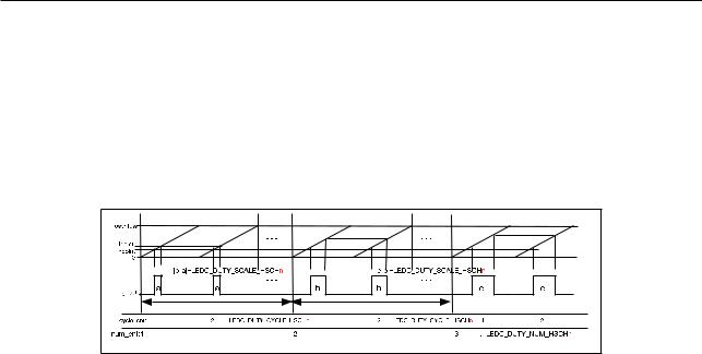
The channels also have the ability to automatically fade from one duty cycle value to another. This feature is enabled by setting LEDC_DUTY_START_HSCHn. When this bit is set, the PWM controller will automatically increment or decrement the value in LEDC_DUTY_HSCHn, depending on whether the bit LEDC_DUTY_INC_HSCHn is set or cleared, respectively. The speed the duty cycle changes is defined as such: every time the LEDC_DUTY_CYCLE_
HSCHn cycles, the content of LEDC_DUTY_SCALE_HSCHn is added to or subtracted from LEDC_DUTY_HSCHn[24..4]. The length of the fade can be limited by setting LEDC_DUTY_NUM_HSCHn: the fade will only last that number of cycles before finishing. A finished fade also generates an interrupt.
Figure 145. Output Signal Diagram of Fading Duty Cycle
Figure 14-5 is an illustration of this. In this configuration, LEDC_DUTY_NUM_HSCHn_R increases by LEDC_DUTY_ SCALE_HSCHn for every LEDC_DUTY_CYCLE_HSCHn clock cycles, which is reflected in the duty cycle of the output signal.
Notes
•When LEDC is in fade mode, configure the second fade only after LEDC_DUTY_CHNG_END_HSCHn or LEDC_DUTY_CHNG_END_LSCHn interrupt is generated.
•When LEDC is in decremental fade mode and LEDC_DUTY_HSCHn is 2LEDC_HSTIMERx_DUTY _RES, LEDC_ DUTY_SCALE_HSCHn cannot be set to 1. When LEDC is in decremental fade mode and LEDC_DUTY_LSCHn is 2LEDC_LSTIMERx_DUTY _RES, LEDC_DUTY_SCALE_LSCHn cannot be set to 1.
14.2.4 Interrupts
•LEDC_DUTY_CHNG_END_LSCHn_INT: Triggered when a fade on a low-speed channel has finished.
•LEDC_DUTY_CHNG_END_HSCHn_INT: Triggered when a fade on a high-speed channel has finished.
•LEDC_HS_TIMERx_OVF_INT: Triggered when a high-speed timer has reached its maximum counter value.
•LEDC_LS_TIMERx_OVF_INT: Triggered when a low-speed timer has reached its maximum counter value.
14.3Register Summary
|
Name |
Description |
Address |
Access |
|
|
Configuration registers |
|
|
|
|
|
|
|
|
|
|
|
LEDC_CONF_REG |
Global ledc configuration register |
0x3FF59190 |
R/W |
|
|
|
|
|
|
|
|
LEDC_HSCH0_CONF0_REG |
Configuration register 0 for high-speed channel 0 |
0x3FF59000 |
R/W |
|
|
|
|
|
|
|
|
LEDC_HSCH1_CONF0_REG |
Configuration register 0 for high-speed channel 1 |
0x3FF59014 |
R/W |
|
|
|
|
|
|
|
|
LEDC_HSCH2_CONF0_REG |
Configuration register 0 for high-speed channel 2 |
0x3FF59028 |
R/W |
|
|
|
|
|
|
|
|
LEDC_HSCH3_CONF0_REG |
Configuration register 0 for high-speed channel 3 |
0x3FF5903C |
R/W |
|
|
|
|
|
|
|
|
LEDC_HSCH4_CONF0_REG |
Configuration register 0 for high-speed channel 4 |
0x3FF59050 |
R/W |
|
|
|
|
|
|
|
Espressif Systems |
388 |
ESP32 TRM (Version 5.0) |
|||
Submit Documentation Feedback

14 LED PWM Controller (LEDC)
|
Name |
Description |
Address |
Access |
|
|
LEDC_HSCH5_CONF0_REG |
Configuration register 0 for high-speed channel 5 |
0x3FF59064 |
R/W |
|
|
|
|
|
|
|
|
LEDC_HSCH6_CONF0_REG |
Configuration register 0 for high-speed channel 6 |
0x3FF59078 |
R/W |
|
|
|
|
|
|
|
|
LEDC_HSCH7_CONF0_REG |
Configuration register 0 for high-speed channel 7 |
0x3FF5908C |
R/W |
|
|
|
|
|
|
|
|
LEDC_HSCH0_CONF1_REG |
Configuration register 1 for high-speed channel 0 |
0x3FF5900C |
R/W |
|
|
|
|
|
|
|
|
LEDC_HSCH1_CONF1_REG |
Configuration register 1 for high-speed channel 1 |
0x3FF59020 |
R/W |
|
|
|
|
|
|
|
|
LEDC_HSCH2_CONF1_REG |
Configuration register 1 for high-speed channel 2 |
0x3FF59034 |
R/W |
|
|
|
|
|
|
|
|
LEDC_HSCH3_CONF1_REG |
Configuration register 1 for high-speed channel 3 |
0x3FF59048 |
R/W |
|
|
|
|
|
|
|
|
LEDC_HSCH4_CONF1_REG |
Configuration register 1 for high-speed channel 4 |
0x3FF5905C |
R/W |
|
|
|
|
|
|
|
|
LEDC_HSCH5_CONF1_REG |
Configuration register 1 for high-speed channel 5 |
0x3FF59070 |
R/W |
|
|
|
|
|
|
|
|
LEDC_HSCH6_CONF1_REG |
Configuration register 1 for high-speed channel 6 |
0x3FF59084 |
R/W |
|
|
|
|
|
|
|
|
LEDC_HSCH7_CONF1_REG |
Configuration register 1 for high-speed channel 7 |
0x3FF59098 |
R/W |
|
|
|
|
|
|
|
|
LEDC_LSCH0_CONF0_REG |
Configuration register 0 for low-speed channel 0 |
0x3FF590A0 |
R/W |
|
|
|
|
|
|
|
|
LEDC_LSCH1_CONF0_REG |
Configuration register 0 for low-speed channel 1 |
0x3FF590B4 |
R/W |
|
|
|
|
|
|
|
|
LEDC_LSCH2_CONF0_REG |
Configuration register 0 for low-speed channel 2 |
0x3FF590C8 |
R/W |
|
|
|
|
|
|
|
|
LEDC_LSCH3_CONF0_REG |
Configuration register 0 for low-speed channel 3 |
0x3FF590DC |
R/W |
|
|
|
|
|
|
|
|
LEDC_LSCH4_CONF0_REG |
Configuration register 0 for low-speed channel 4 |
0x3FF590F0 |
R/W |
|
|
|
|
|
|
|
|
LEDC_LSCH5_CONF0_REG |
Configuration register 0 for low-speed channel 5 |
0x3FF59104 |
R/W |
|
|
|
|
|
|
|
|
LEDC_LSCH6_CONF0_REG |
Configuration register 0 for low-speed channel 6 |
0x3FF59118 |
R/W |
|
|
|
|
|
|
|
|
LEDC_LSCH7_CONF0_REG |
Configuration register 0 for low-speed channel 7 |
0x3FF5912C |
R/W |
|
|
|
|
|
|
|
|
LEDC_LSCH0_CONF1_REG |
Configuration register 1 for low-speed channel 0 |
0x3FF590AC |
R/W |
|
|
|
|
|
|
|
|
LEDC_LSCH1_CONF1_REG |
Configuration register 1 for low-speed channel 1 |
0x3FF590C0 |
R/W |
|
|
|
|
|
|
|
|
LEDC_LSCH2_CONF1_REG |
Configuration register 1 for low-speed channel 2 |
0x3FF590D4 |
R/W |
|
|
|
|
|
|
|
|
LEDC_LSCH3_CONF1_REG |
Configuration register 1 for low-speed channel 3 |
0x3FF590E8 |
R/W |
|
|
|
|
|
|
|
|
LEDC_LSCH4_CONF1_REG |
Configuration register 1 for low-speed channel 4 |
0x3FF590FC |
R/W |
|
|
|
|
|
|
|
|
LEDC_LSCH5_CONF1_REG |
Configuration register 1 for low-speed channel 5 |
0x3FF59110 |
R/W |
|
|
|
|
|
|
|
|
LEDC_LSCH6_CONF1_REG |
Configuration register 1 for low-speed channel 6 |
0x3FF59124 |
R/W |
|
|
|
|
|
|
|
|
LEDC_LSCH7_CONF1_REG |
Configuration register 1 for low-speed channel 7 |
0x3FF59138 |
R/W |
|
|
|
|
|
|
|
|
Dutycycle registers |
|
|
|
|
|
|
|
|
|
|
|
LEDC_HSCH0_DUTY_REG |
Initial duty cycle for high-speed channel 0 |
0x3FF59008 |
R/W |
|
|
|
|
|
|
|
|
LEDC_HSCH1_DUTY_REG |
Initial duty cycle for high-speed channel 1 |
0x3FF5901C |
R/W |
|
|
|
|
|
|
|
|
LEDC_HSCH2_DUTY_REG |
Initial duty cycle for high-speed channel 2 |
0x3FF59030 |
R/W |
|
|
|
|
|
|
|
|
LEDC_HSCH3_DUTY_REG |
Initial duty cycle for high-speed channel 3 |
0x3FF59044 |
R/W |
|
|
|
|
|
|
|
|
LEDC_HSCH4_DUTY_REG |
Initial duty cycle for high-speed channel 4 |
0x3FF59058 |
R/W |
|
|
|
|
|
|
|
|
LEDC_HSCH5_DUTY_REG |
Initial duty cycle for high-speed channel 5 |
0x3FF5906C |
R/W |
|
|
|
|
|
|
|
|
LEDC_HSCH6_DUTY_REG |
Initial duty cycle for high-speed channel 6 |
0x3FF59080 |
R/W |
|
|
|
|
|
|
|
|
LEDC_HSCH7_DUTY_REG |
Initial duty cycle for high-speed channel 7 |
0x3FF59094 |
R/W |
|
|
|
|
|
|
|
|
LEDC_HSCH0_DUTY_R_REG |
Current duty cycle for high-speed channel 0 |
0x3FF59010 |
RO |
|
|
|
|
|
|
|
|
LEDC_HSCH1_DUTY_R_REG |
Current duty cycle for high-speed channel 1 |
0x3FF59024 |
RO |
|
|
|
|
|
|
|
|
LEDC_HSCH2_DUTY_R_REG |
Current duty cycle for high-speed channel 2 |
0x3FF59038 |
RO |
|
|
|
|
|
|
|
|
LEDC_HSCH3_DUTY_R_REG |
Current duty cycle for high-speed channel 3 |
0x3FF5904C |
RO |
|
|
|
|
|
|
|
|
LEDC_HSCH4_DUTY_R_REG |
Current duty cycle for high-speed channel 4 |
0x3FF59060 |
RO |
|
|
|
|
|
|
|
|
LEDC_HSCH5_DUTY_R_REG |
Current duty cycle for high-speed channel 5 |
0x3FF59074 |
RO |
|
|
|
|
|
|
|
|
LEDC_HSCH6_DUTY_R_REG |
Current duty cycle for high-speed channel 6 |
0x3FF59088 |
RO |
|
|
|
|
|
|
|
Espressif Systems |
389 |
ESP32 TRM (Version 5.0) |
|||
Submit Documentation Feedback

14 LED PWM Controller (LEDC)
Name |
Description |
Address |
Access |
LEDC_HSCH7_DUTY_R_REG |
Current duty cycle for high-speed channel 7 |
0x3FF5909C |
RO |
|
|
|
|
LEDC_LSCH0_DUTY_REG |
Initial duty cycle for low-speed channel 0 |
0x3FF590A8 |
R/W |
|
|
|
|
LEDC_LSCH1_DUTY_REG |
Initial duty cycle for low-speed channel 1 |
0x3FF590BC |
R/W |
|
|
|
|
LEDC_LSCH2_DUTY_REG |
Initial duty cycle for low-speed channel 2 |
0x3FF590D0 |
R/W |
|
|
|
|
LEDC_LSCH3_DUTY_REG |
Initial duty cycle for low-speed channel 3 |
0x3FF590E4 |
R/W |
|
|
|
|
LEDC_LSCH4_DUTY_REG |
Initial duty cycle for low-speed channel 4 |
0x3FF590F8 |
R/W |
|
|
|
|
LEDC_LSCH5_DUTY_REG |
Initial duty cycle for low-speed channel 5 |
0x3FF5910C |
R/W |
|
|
|
|
LEDC_LSCH6_DUTY_REG |
Initial duty cycle for low-speed channel 6 |
0x3FF59120 |
R/W |
|
|
|
|
LEDC_LSCH7_DUTY_REG |
Initial duty cycle for low-speed channel 7 |
0x3FF59134 |
R/W |
|
|
|
|
LEDC_LSCH0_DUTY_R_REG |
Current duty cycle for low-speed channel 0 |
0x3FF590B0 |
RO |
|
|
|
|
LEDC_LSCH1_DUTY_R_REG |
Current duty cycle for low-speed channel 1 |
0x3FF590C4 |
RO |
|
|
|
|
LEDC_LSCH2_DUTY_R_REG |
Current duty cycle for low-speed channel 2 |
0x3FF590D8 |
RO |
|
|
|
|
LEDC_LSCH3_DUTY_R_REG |
Current duty cycle for low-speed channel 3 |
0x3FF590EC |
RO |
|
|
|
|
LEDC_LSCH4_DUTY_R_REG |
Current duty cycle for low-speed channel 4 |
0x3FF59100 |
RO |
|
|
|
|
LEDC_LSCH5_DUTY_R_REG |
Current duty cycle for low-speed channel 5 |
0x3FF59114 |
RO |
|
|
|
|
LEDC_LSCH6_DUTY_R_REG |
Current duty cycle for low-speed channel 6 |
0x3FF59128 |
RO |
|
|
|
|
LEDC_LSCH7_DUTY_R_REG |
Current duty cycle for low-speed channel 7 |
0x3FF5913C |
RO |
|
|
|
|
Timer registers |
|
|
|
|
|
|
|
LEDC_HSTIMER0_CONF_REG |
High-speed timer 0 configuration |
0x3FF59140 |
R/W |
|
|
|
|
LEDC_HSTIMER1_CONF_REG |
High-speed timer 1 configuration |
0x3FF59148 |
R/W |
|
|
|
|
LEDC_HSTIMER2_CONF_REG |
High-speed timer 2 configuration |
0x3FF59150 |
R/W |
|
|
|
|
LEDC_HSTIMER3_CONF_REG |
High-speed timer 3 configuration |
0x3FF59158 |
R/W |
|
|
|
|
LEDC_HSTIMER0_VALUE_REG |
High-speed timer 0 current counter value |
0x3FF59144 |
RO |
|
|
|
|
LEDC_HSTIMER1_VALUE_REG |
High-speed timer 1 current counter value |
0x3FF5914C |
RO |
|
|
|
|
LEDC_HSTIMER2_VALUE_REG |
High-speed timer 2 current counter value |
0x3FF59154 |
RO |
|
|
|
|
LEDC_HSTIMER3_VALUE_REG |
High-speed timer 3 current counter value |
0x3FF5915C |
RO |
|
|
|
|
LEDC_LSTIMER0_CONF_REG |
Low-speed timer 0 configuration |
0x3FF59160 |
R/W |
|
|
|
|
LEDC_LSTIMER1_CONF_REG |
Low-speed timer 1 configuration |
0x3FF59168 |
R/W |
|
|
|
|
LEDC_LSTIMER2_CONF_REG |
Low-speed timer 2 configuration |
0x3FF59170 |
R/W |
|
|
|
|
LEDC_LSTIMER3_CONF_REG |
Low-speed timer 3 configuration |
0x3FF59178 |
R/W |
|
|
|
|
LEDC_LSTIMER0_VALUE_REG |
Low-speed timer 0 current counter value |
0x3FF59164 |
RO |
|
|
|
|
LEDC_LSTIMER1_VALUE_REG |
Low-speed timer 1 current counter value |
0x3FF5916C |
RO |
|
|
|
|
LEDC_LSTIMER2_VALUE_REG |
Low-speed timer 2 current counter value |
0x3FF59174 |
RO |
|
|
|
|
LEDC_LSTIMER3_VALUE_REG |
Low-speed timer 3 current counter value |
0x3FF5917C |
RO |
|
|
|
|
Interrupt registers |
|
|
|
|
|
|
|
LEDC_INT_RAW_REG |
Raw interrupt status |
0x3FF59180 |
RO |
|
|
|
|
LEDC_INT_ST_REG |
Masked interrupt status |
0x3FF59184 |
RO |
|
|
|
|
LEDC_INT_ENA_REG |
Interrupt enable bits |
0x3FF59188 |
R/W |
|
|
|
|
LEDC_INT_CLR_REG |
Interrupt clear bits |
0x3FF5918C |
WO |
|
|
|
|
Espressif Systems |
390 |
ESP32 TRM (Version 5.0) |
Submit Documentation Feedback
14 LED PWM Controller (LEDC)
14.4Registers
The addresses in parenthesis besides register names are the register addresses relative to the LED PWM base address provided in Table 1-6 Peripheral Address Mapping in Chapter 1 System and Memory. The absolute register addresses are listed in Section 14.3 Register Summary.
Register 14.1. LEDC_HSCHn_CONF0_REG (n: 07) (0x1C+0x10*n)
|
|
|
|
|
|
|
|
|
|
n |
|
|
n |
|
|
|
|
|
|
|
|
|
|
|
|
|
HSCH |
|
n |
||
|
|
|
|
|
|
|
HSCH_ |
_ |
|
HSCH |
|||||
|
|
|
|
|
|
|
|
|
_ |
|
|||||
|
|
|
|
|
|
|
|
|
|
EN |
|
|
|||
|
|
|
|
|
_ |
_ |
OUT |
|
|
SEL |
|
|
|||
|
|
|
|
|
|
|
|
|
_ |
|
|
|
|||
|
|
|
|
|
LV |
|
|
|
|
|
|
|
|
||
|
|
|
IDLE SIG |
|
TIMER |
|
|
|
|||||||
(reserved) |
|
LEDCLEDC |
|
|
_ |
|
|
|
|
|
|
|
|
||
|
|
LEDC |
|
|
|
|
|
|
|||||||
|
|
|
_ |
_ |
|
|
_ |
|
|
|
|
|
|
||
|
|
|
|
|
|
|
|
|
|
|
|
|
|
|
|
31 |
4 |
3 |
2 |
1 |
|
|
|
0 |
|
|
|
|
|
|
|
|
|
|
|
|
|
|
|
|
Reset |
|
|
|
|||
|
|
|
|
|
|
|
|
|
|
|
|
||||
0x00000000 |
|
0 |
0 |
|
|
0 |
|
|
|
|
|
||||
LEDC_IDLE_LV_HSCHn This bit is used to control the output value when high-speed channel n is inactive. (R/W)
LEDC_SIG_OUT_EN_HSCHn This is the output enable control bit for high-speed channel n. (R/W)
LEDC_TIMER_SEL_HSCHn There are four high-speed timers. These two bits are used to select one of them for high-speed channel n: (R/W)
0:select hstimer0;
1:select hstimer1;
2:select hstimer2;
3:select hstimer3.
Register 14.2. LEDC_HSCHn_HPOINT_REG (n: 07) (0x20+0x10*n)
|
|
|
n |
|
|
|
|
|
HSCH |
|
|
|
|
|
_ |
|
|
|
(reserved) |
|
HPOINT |
|
|
|
|
LEDC |
|
|
|
|
|
|
_ |
|
|
|
|
|
|
|
|
31 |
20 |
19 |
|
0 |
|
|
|
|
|
|
Reset |
|
|
|
|
|
|
|
0x0000 |
|
0x000000 |
|
LEDC_HPOINT_HSCHn The output value changes to high when htimerx(x=[0,3]), selected by highspeed channel n, has reached LEDC_HPOINT_HSCHn[19:0]. (R/W)
Espressif Systems |
391 |
ESP32 TRM (Version 5.0) |
Submit Documentation Feedback

14 LED PWM Controller (LEDC)
|
Register 14.3. LEDC_HSCHn_DUTY_REG (n: 07) (0x24+0x10*n) |
|
|
|
|
|
n |
|
|
|
|
HSCH |
|
|
|
|
_ |
|
|
(reserved) |
|
DUTY |
|
|
|
LEDC |
|
|
|
|
|
_ |
|
|
|
|
|
|
|
31 |
25 |
24 |
0 |
|
|
|
|
|
Reset |
|
|
|
|
|
0x00 |
|
0x0000000 |
|
|
LEDC_DUTY_HSCHn The register is used to control output duty. When hstimerx(x=[0,3]), selected by high-speed channel n, has reached LEDC_LPOINT_HSCHn, the output signal changes to low. (R/W)
LEDC_LPOINT_HSCHn=LEDC_LPOINT_HSCHn[19:0]+LEDC_DUTY_HSCHn[24:4] (1) LEDC_LPOINT_HSCHn=LEDC_LPOINT_HSCHn[19:0]+LEDC_DUTY_HSCHn[24:4] +1) (2) See the Functional Description for more information on when (1) or (2) is chosen.
Register 14.4. LEDC_HSCHn_CONF1_REG (n: 07) (0x28+0x10*n)
|
|
|
|
n |
|
|
|
|
n |
|
n |
|
|
|
|
HSCH |
n |
n |
|
HSCH |
|
HSCH |
|||
|
|
|
|
|
HSCH |
|
|
|
|
|
|
|
|
|
|
_ |
HSCH |
|
_ |
|
|
_ |
|
||
|
|
|
|
_ |
|
CYCLE |
|
|
SCALE |
|||
|
|
STARTINC |
|
NUM |
|
|
|
|||||
|
|
|
|
_ |
|
|
|
|
|
|
|
|
|
|
_ |
_ |
|
|
_ |
|
_ |
|
|
_ |
|
|
DUTYDUTY |
|
|
DUTY |
|
DUTY |
|
|
DUTY |
|||
|
_ |
_ |
|
|
|
_ |
|
_ |
|
_ |
|
|
LEDCLEDC |
|
|
|
LEDC |
|
LEDC |
|
LEDC |
|
|
||
31 |
30 |
29 |
|
|
|
20 |
19 |
10 |
9 |
|
0 |
|
|
|
|
|
|
|
|
|
|
|
|
|
Reset |
|
|
|
|
|
|
|
|
|
|
|
|
|
0 |
1 |
|
|
|
|
0x000 |
|
0x000 |
|
0x000 |
|
|
LEDC_DUTY_START_HSCHn When LEDC_DUTY_NUM_HSCHn, LEDC_DUTY_CYCLE_HSCHn and LEDC_DUTY_SCALE_HSCHn has been configured, these register will not take effect until LEDC_DUTY_START_HSCHn is set. This bit is automatically cleared by hardware. (R/W)
LEDC_DUTY_INC_HSCHn This register is used to increase or decrease the duty of output signal for high-speed channel n. (R/W)
LEDC_DUTY_NUM_HSCHn This register is used to control the number of times the duty cycle is increased or decreased for high-speed channel n. (R/W)
LEDC_DUTY_CYCLE_HSCHn This register is used to increase or decrease the duty cycle every time LEDC_DUTY_CYCLE_HSCHn cycles for high-speed channel n. (R/W)
LEDC_DUTY_SCALE_HSCHn This register is used to increase or decrease the step scale for highspeed channel n. (R/W)
Espressif Systems |
392 |
ESP32 TRM (Version 5.0) |
Submit Documentation Feedback

14 LED PWM Controller (LEDC)
Register 14.5. LEDC_HSCHn_DUTY_R_REG (n: 07) (0x2C+0x10*n)
|
|
|
|
R |
|
|
|
|
|
_ |
|
|
|
|
|
|
n |
|
|
|
|
|
|
HSCH |
|
|
|
|
|
|
_ |
|
|
|
|
(reserved) |
|
DUTY |
|
|
|
|
|
LEDC |
|
|
|
|
|
|
|
_ |
|
|
|
|
|
|
|
|
|
|
31 |
25 |
24 |
|
|
0 |
|
|
|
|
|
|
|
Reset |
|
|
|
|
|
|
|
|
0x00 |
|
0x0000000 |
|
|
|
LEDC_DUTY_HSCHn_R This register represents the current duty cycle of the output signal for highspeed channel n. (RO)
Register 14.6. LEDC_LSCHn_CONF0_REG (n: 07) (0xBC+0x10*n)
|
|
|
|
|
|
|
|
|
|
|
n |
|
|
n |
|
|
|
|
|
|
|
|
|
|
|
|
|
|
LSCH |
|
n |
||
|
|
|
|
|
|
|
|
|
n |
|
|
_ |
|
LSCH |
||
|
|
|
|
|
|
LSCH |
|
|
|
|
_ |
|
||||
|
|
|
|
|
_ |
|
LSCH_ |
|
|
|
|
|
||||
|
|
|
|
|
|
|
|
|
EN |
SEL |
|
|
||||
|
|
|
|
UP |
|
_ |
OUT |
|
|
|
|
|||||
|
|
|
|
_ |
|
|
|
|
_ |
|
|
|
||||
|
|
|
|
_ |
|
|
|
|
|
|
|
|
|
|||
|
|
|
|
|
LV |
|
|
TIMER |
|
|
|
|||||
|
|
|
PARAIDLE SIG |
|
|
|
|
|||||||||
(reserved) |
|
LEDCLEDCLEDC |
|
|
_ |
|
|
|
|
|
|
|
||||
|
|
LEDC |
|
|
|
|
|
|
|
|||||||
|
|
|
_ |
_ |
_ |
|
|
_ |
|
|
|
|
|
|
||
|
|
|
|
|
|
|
|
|
|
|
|
|
|
|
|
|
31 |
5 |
4 |
3 |
2 |
1 |
|
|
|
0 |
|
|
|
|
|
|
|
|
|
|
|
|
|
|
|
|
|
Reset |
|
|
|
|||
|
|
|
|
|
|
|
|
|
|
|
|
|
||||
0x0000000 |
|
0 |
0 |
0 |
|
|
0 |
|
|
|
|
|
||||
LEDC_PARA_UP_LSCHn This bit is used to update |
register LEDC_LSCHn_HPOINT |
|
|
and |
|
|
|
|
|
|||||||
LEDC_LSCHn_DUTY for low-speed channel n. (R/W) |
|
|
|
|
|
|
|
|
|
|
|
|
|
|
|
|
LEDC_IDLE_LV_LSCHn This bit is used to control the output value, when low-speed channel n is inactive. (R/W)
LEDC_SIG_OUT_EN_LSCHn This is the output enable control bit for low-speed channel n. (R/W)
LEDC_TIMER_SEL_LSCHn There are four low-speed timers, the two bits are used to select one of them for low-speed channel n. (R/W)
0:select lstimer0;
1:select lstimer1;
2:select lstimer2;
3:select lstimer3.
Espressif Systems |
393 |
ESP32 TRM (Version 5.0) |
Submit Documentation Feedback

14 LED PWM Controller (LEDC)
Register 14.7. LEDC_LSCHn_HPOINT_REG (n: 07) (0xC0+0x10*n)
|
|
|
n |
|
|
|
|
|
LSCH |
|
|
|
|
|
_ |
|
|
|
(reserved) |
|
HPOINT |
|
|
|
|
LEDC |
|
|
|
|
|
|
_ |
|
|
|
|
|
|
|
|
31 |
20 |
19 |
|
0 |
|
|
|
|
|
|
Reset |
|
|
|
|
|
|
|
0x0000 |
|
0x000000 |
|
LEDC_HPOINT_LSCHn The output value changes to high when lstimerx(x=[0,3]), selected by lowspeed channel n, has reached LEDC_HPOINT_LSCHn[19:0]. (R/W)
|
Register 14.8. LEDC_LSCHn_DUTY_REG (n: 07) (0xC4+0x10*n) |
|
|
|
|
|
n |
|
|
|
|
LSCH |
|
|
|
|
_ |
|
|
(reserved) |
|
DUTY |
|
|
|
LEDC |
|
|
|
|
|
_ |
|
|
|
|
|
|
|
31 |
25 |
24 |
0 |
|
|
|
|
|
Reset |
|
|
|
|
|
0x00 |
|
0x0000000 |
|
|
LEDC_DUTY_LSCHn The register is used to control output duty. When lstimerx(x=[0,3]), chosen by low-speed channel n, has reached LEDC_LPOINT_LSCHn,the output signal changes to low. (R/W) LEDC_LPOINT_LSCHn=(LEDC_HPOINT_LSCHn[19:0]+LEDC_DUTY_LSCHn[24:4]) (1)
LEDC_LPOINT_LSCHn=(LEDC_HPOINT_LSCHn[19:0]+LEDC_DUTY_LSCHn[24:4] +1) (2) See the Functional Description for more information on when (1) or (2) is chosen.
Espressif Systems |
394 |
ESP32 TRM (Version 5.0) |
Submit Documentation Feedback

14 LED PWM Controller (LEDC)
Register 14.9. LEDC_LSCHn_CONF1_REG (n: 07) (0xC8+0x10*n)
|
|
|
|
n |
|
|
|
n |
|
|
n |
||
|
|
|
LSCH |
n |
n |
|
LSCH |
|
|
LSCH |
|||
|
|
|
|
|
LSCH |
|
|
|
|
|
|
|
|
|
|
|
_ |
LSCH |
|
_ |
|
|
|
_ |
|
||
|
|
|
|
_ |
|
CYCLE |
|
|
SCALE |
||||
|
|
STARTINC |
|
NUM |
|
|
|
||||||
|
|
|
|
_ |
|
|
|
|
|
|
|
|
|
|
|
_ |
_ |
|
|
_ |
|
_ |
|
|
|
_ |
|
|
DUTYDUTY |
|
|
DUTY |
|
DUTY |
|
|
DUTY |
||||
|
_ |
_ |
|
|
|
_ |
|
_ |
|
|
_ |
|
|
LEDCLEDC |
|
|
|
LEDC |
|
LEDC |
|
LEDC |
|
|
|||
31 |
30 |
29 |
|
|
|
20 |
19 |
10 |
|
9 |
|
0 |
|
|
|
|
|
|
|
|
|
|
|
|
|
|
Reset |
|
|
|
|
|
|
|
|
|
|
|
|
|
|
0 |
1 |
|
|
|
|
0x000 |
|
0x000 |
|
|
0x000 |
|
|
LEDC_DUTY_START_LSCHn When LEDC_DUTY_NUM_HSCHn, LEDC_DUTY_CYCLE_HSCHn and LEDC_DUTY_SCALE_HSCHn have been configured, these settings will not take effect until set LEDC_DUTY_START_HSCHn. This bit is automatically cleared by hardware. (R/W)
LEDC_DUTY_INC_LSCHn This register is used to increase or decrease the duty of output signal for low-speed channel n. (R/W)
LEDC_DUTY_NUM_LSCHn This register is used to control the number of times the duty cycle is increased or decreased for low-speed channel n. (R/W)
LEDC_DUTY_CYCLE_LSCHn This register is used to increase or decrease the duty every LEDC_DUTY_CYCLE_LSCHn cycles for low-speed channel n. (R/W)
LEDC_DUTY_SCALE_LSCHn This register is used to increase or decrease the step scale for lowspeed channel n. (R/W)
Register 14.10. LEDC_LSCHn_DUTY_R_REG (n: 07) (0xCC+0x10*n)
|
|
|
|
R |
|
|
|
|
|
_ |
|
|
|
|
|
|
n |
|
|
|
|
|
|
LSCH |
|
|
|
|
|
|
_ |
|
|
|
|
(reserved) |
|
DUTY |
|
|
|
|
|
LEDC |
|
|
|
|
|
|
|
_ |
|
|
|
|
|
|
|
|
|
|
31 |
25 |
24 |
|
|
0 |
|
|
|
|
|
|
|
Reset |
|
|
|
|
|
|
|
|
0x00 |
|
0x0000000 |
|
|
|
LEDC_DUTY_LSCHn_R This register represents the current duty of the output signal for low-speed channel n. (RO)
Espressif Systems |
395 |
ESP32 TRM (Version 5.0) |
Submit Documentation Feedback

14 LED PWM Controller (LEDC)
Register 14.11. LEDC_HSTIMERx_CONF_REG (x: 03) (0x140+8*x)
|
|
|
|
|
|
|
|
|
x |
|
|
|
|
|
_ |
|
|
|
|
|
|
|
|
|
HSTIMER |
|
|
|
|
|
|
|
|
|
|
|
|
|
x |
|
|
|
|
|
|
|
RES |
|
|
|
|
|
HSTIMER _ |
|
|
|
|
|
_ |
||||
|
|
|
|
|
|
|
RST |
PAUSE |
_ |
|
|
|
|
|
DUTY |
|
|
|
|
|
_ |
x |
x |
|
NUM |
|
|
|
x |
|
|
|
|
|
|
SEL |
|
|
|
_ |
|
|
HSTIMER |
|
|
||
|
|
|
|
|
|
|
CLK |
|
|
|
|
||||
|
|
|
TICK HSTIMERHSTIMER |
|
|
|
|
|
|||||||
|
|
|
|
_ |
|
|
|
|
DIV |
|
|
|
|
|
|
(reserved) |
|
LEDCLEDCLEDC |
|
|
|
_ |
|
LEDC |
|
|
|||||
|
|
|
|
LEDC |
|
|
|
||||||||
|
|
|
_ |
_ |
_ |
|
|
|
_ |
|
|
_ |
|
|
|
|
|
|
|
|
|
|
|
|
|
|
|
|
|
|
|
31 |
26 |
25 |
24 |
23 |
22 |
|
|
|
|
5 |
4 |
0 |
|
|
|
|
|
|
|
|
|
|
|
|
|
|
|
|
Reset |
||
|
|
|
|
|
|
|
|
|
|
|
|
|
|||
0x00 |
|
0 |
1 |
0 |
|
|
|
|
0x00000 |
|
0x00 |
|
|||
LEDC_TICK_SEL_HSTIMERx This bit is used to select APB_CLK or REF_TICK for high-speed timer x. (R/W)
1: APB_CLK;
0: REF_TICK.
LEDC_HSTIMERx_RST This bit is used to reset high-speed timer x. The counter value will be ’zero’ after reset. (R/W)
LEDC_HSTIMERx_PAUSE This bit is used to suspend the counter in high-speed timer x. (R/W)
LEDC_CLK_DIV_NUM_HSTIMERx This register is used to configure the division factor for the divider in high-speed timer x. The least significant eight bits represent the fractional part. (R/W)
LEDC_HSTIMERx_DUTY_RES This register is used to control the range of the counter in high-speed timer x. The counter range is [0, 2LEDC_HSTIMERx_DUTY _RES], the maximum bit width for counter is 20. (R/W)
Register 14.12. LEDC_HSTIMERx_VALUE_REG (x: 03) (0x144+8*x)
|
|
|
|
|
|
|
|
|
|
|
|
|
|
|
|
CNT |
|
|
|
|
|
|
|
|
|
|
|
|
|
|
|
|
|
|
|
|
|
|
_ |
|
|
|
|
|
|
|
|
|
|
|
|
|
|
|
|
|
|
|
|
|
|
x |
|
|
|
|
|
|
|
|
|
(reserved) |
|
|
|
|
|
|
|
|
|
|
|
|
HSTIMER |
|
|
|
|
|
|
|
|
|
|
|
|
|
|
|
|
|
|
|
|
|
LEDC |
|
|
|
|
|
|
|
|
|
|
||
|
|
|
|
|
|
|
|
|
|
|
|
|
_ |
|
|
|
|
|
|
|
|
|
|
|
|
|
|
|
|
|
|
|
|
|
|
|
|
|
|
|
|
|
|
|
|
|
|
31 |
20 |
19 |
|
|
|
|
|
|
|
|
|
|
|
|
|
|
|
|
|
|
|
0 |
|
|
|
|
|
|
|
|
|
|
|
|
|
|
|
|
|
|
|
|
|
|
|
|
Reset |
|
|
|
|
|
|
|
|
|
|
|
|
|
|
|
|
|
|
|
|
|
|
|
|
0x0000 |
|
0 |
0 |
0 |
0 |
0 |
0 |
0 |
0 |
0 |
0 |
0 |
0 |
0 |
|
0 |
0 |
0 |
0 |
0 |
0 |
0 |
|
LEDC_HSTIMERx_CNT Software can read this register to get the current counter value of high-speed timer x. (RO)
Espressif Systems |
396 |
ESP32 TRM (Version 5.0) |
Submit Documentation Feedback

14 LED PWM Controller (LEDC)
Register 14.13. LEDC_LSTIMERx_CONF_REG (x: 03) (0x160+8*x)
|
|
|
|
|
|
|
|
|
|
|
x |
|
|
|
|
|
_ |
|
|
|
|
|
|
|
|
UP |
|
|
LSTIMER |
|
|
|
|
|
|
|
|
|
|
|
|
|
|
x |
|
|
|
|
|
|
RES |
||
|
|
|
|
|
|
PARALSTIMERRST PAUSE |
_ |
|
|
|
|
|
DUTY |
||||
|
|
|
|
|
_ |
_ |
_ |
|
_ |
NUM |
|
|
|
|
_ |
||
|
|
|
|
|
x |
SEL |
x |
x |
_ |
|
|
|
x |
|
|||
|
|
|
LSTIMERTICK |
|
|
|
CLK |
|
LSTIMER |
|
|
||||||
|
|
|
LSTIMERLSTIMER |
|
|
|
|
||||||||||
|
|
|
|
|
_ |
|
|
|
|
DIV |
|
|
|
|
|
|
|
(reserved) |
|
LEDCLEDCLEDCLEDC |
|
|
|
_ |
|
LEDC |
|
|
|
|
|||||
|
|
|
|
LEDC |
|
|
|
|
|
||||||||
|
|
|
_ |
_ |
_ |
_ |
|
|
|
_ |
|
_ |
|
|
|
|
|
|
|
|
|
|
|
|
|
|
|
|
|
|
|
|
|
|
|
31 |
27 |
26 |
25 |
24 |
23 |
22 |
|
|
|
5 |
4 |
|
0 |
|
|
|
|
|
|
|
|
|
|
|
|
|
|
|
|
|
|
Reset |
|||
|
|
|
|
|
|
|
|
|
|
|
|
|
|
|
|||
0x00 |
|
0 |
0 |
1 |
0 |
|
|
|
|
0x00000 |
|
0x00 |
|
||||
LEDC_LSTIMERx_PARA_UP Set this bit |
to update LEDC_CLK_DIV_NUM_LSTIMEx |
and |
|
||||||||||||||
LEDC_LSTIMERx_DUTY_RES. (R/W) |
|
|
|
|
|
|
|
||||||||||
LEDC_TICK_SEL_LSTIMERx This bit is used to select RTC_SLOW_CLK or REF_TICK for low-speed timer x. (R/W)
1: RTC_SLOW_CLK; 0: REF_TICK.
LEDC_LSTIMERx_RST This bit is used to reset low-speed timer x. The counter will show 0 after reset. (R/W)
LEDC_LSTIMERx_PAUSE This bit is used to suspend the counter in low-speed timer x. (R/W)
LEDC_CLK_DIV_NUM_LSTIMERx This register is used to configure the division factor for the divider in low-speed timer x. The least significant eight bits represent the fractional part. (R/W)
LEDC_LSTIMERx_DUTY_RES This register is used to control the range of the counter in low-speed timer x. The counter range is [0, 2LEDC_LSTIMERx_DUTY _RES], the max bit width for counter is 20. (R/W)
Register 14.14. LEDC_LSTIMERx_VALUE_REG (x: 03) (0x164+8*x)
|
|
|
|
|
|
|
|
|
|
|
|
|
|
|
|
CNT |
|
|
|
|
|
|
|
|
|
|
|
|
|
|
|
|
|
|
|
|
|
|
_ |
|
|
|
|
|
|
|
|
|
|
|
|
|
|
|
|
|
|
|
|
|
|
x |
|
|
|
|
|
|
|
|
|
(reserved) |
|
|
|
|
|
|
|
|
|
|
|
|
LSTIMER |
|
|
|
|
|
|
|
|
|
|
|
|
|
|
|
|
|
|
|
|
|
LEDC |
|
|
|
|
|
|
|
|
|
|
||
|
|
|
|
|
|
|
|
|
|
|
|
|
_ |
|
|
|
|
|
|
|
|
|
|
|
|
|
|
|
|
|
|
|
|
|
|
|
|
|
|
|
|
|
|
|
|
|
|
31 |
20 |
19 |
|
|
|
|
|
|
|
|
|
|
|
|
|
|
|
|
|
|
|
0 |
|
|
|
|
|
|
|
|
|
|
|
|
|
|
|
|
|
|
|
|
|
|
|
|
Reset |
|
|
|
|
|
|
|
|
|
|
|
|
|
|
|
|
|
|
|
|
|
|
|
|
0x0000 |
|
0 |
0 |
0 |
0 |
0 |
0 |
0 |
0 |
0 |
0 |
0 |
0 |
0 |
|
0 |
0 |
0 |
0 |
0 |
0 |
0 |
|
LEDC_LSTIMERx_CNT Software can read this register to get the current counter value of low-speed timer x. (RO)
Espressif Systems |
397 |
ESP32 TRM (Version 5.0) |
Submit Documentation Feedback

14 LED PWM Controller (LEDC)
Register 14.15. LEDC_INT_RAW_REG (0x0180)
|
|
|
|
|
|
|
|
|
|
|
|
|
|
|
|
|
|
|
|
RAW RAW RAW RAW RAW RAW RAW RAW RAW RAW RAW RAW RAW RAW RAW RAW |
|
|
|
|
|
|
|
|
|
||||||||||||||||||||||||||||||||||||||
|
|
|
|
|
|
|
|
|
|
|
|
|
|
|
|
|
|
_ |
|
|
_ |
_ |
_ |
_ |
_ |
_ |
_ |
_ |
_ |
|
_ |
_ |
|
|
_ |
|
_ |
|
_ |
_ |
|
|
|
|
|
|
|
|
|
|
|
||||||||||||||||
|
|
|
|
|
|
|
|
|
|
|
|
|
|
|
|
|
INT |
|
INT INT INT INT INT INT INT INT INT |
|
INT |
|
INT |
|
INT INT INT |
|
INT |
|
|
|
|
|
|
|
|
|
|
|
|||||||||||||||||||||||||||||
|
|
|
|
|
|
|
|
|
|
|
|
|
|
|
|
_ |
|
|
_ |
|
_ |
_ |
_ |
_ |
_ |
_ |
_ |
_ |
|
|
_ |
|
|
_ |
|
_ |
|
_ |
|
_ |
|
_ |
|
|
|
|
|
|
|
|
|
|
|
|
|||||||||||||
|
|
|
|
|
|
|
|
|
|
|
|
|
|
|
LSCH7LSCH6LSCH5LSCH4LSCH3LSCH2LSCH1LSCH0HSCH7HSCH6HSCH5HSCH4HSCH3HSCH2HSCH1HSCH0 |
|
_ |
|
_ |
_ |
_ |
_ |
_ |
_ |
|||||||||||||||||||||||||||||||||||||||||||
|
|
|
|
|
|
|
|
|
|
|
|
|
|
|
|
|
|
|
|
|
|
|
|
|
|
|
|
|
|
|
|
|
|
|
|
|
|
|
|
|
|
|
|
|
|
|
|
|
|
|
INT |
RAW RAW RAW RAW |
RAW RAW RAW RAW |
||||||||||||||
|
|
|
|
|
|
|
|
|
|
|
|
|
|
_ |
_ |
_ |
|
_ |
|
_ |
_ |
_ |
_ |
_ |
_ |
_ |
_ |
|
|
_ |
|
_ |
|
_ |
_ |
|
INT |
INT INT |
INT |
|
|
INT |
|
INT |
|
INT |
|||||||||||||||||||||
|
|
|
|
|
|
|
|
|
|
|
|
|
END END END END END END END END END END END END END END END END |
_ |
|
_ |
_ |
_ |
_ |
|
_ |
|
_ |
|
_ |
||||||||||||||||||||||||||||||||||||||||||
|
|
|
|
|
|
|
|
|
|
|
|
_ |
_ |
_ |
_ |
|
_ |
|
_ |
_ |
_ |
_ |
_ |
_ |
_ |
_ |
|
|
_ |
|
_ |
|
_ |
OVF OVF |
OVF |
OVF OVF |
OVF |
OVF |
OVF |
|
|||||||||||||||||||||||||||
|
|
|
|
|
|
|
|
|
|
CHNGCHNGCHNGCHNGCHNGCHNGCHNGCHNGCHNGCHNGCHNGCHNGCHNGCHNGCHNGCHNG |
_ |
|
_ |
|
_ |
_ |
_ |
_ |
|
|
_ |
|
_ |
|
|
|
|||||||||||||||||||||||||||||||||||||||||
|
|
|
|
|
|
|
|
|
DUTYDUTYDUTYDUTYDUTYDUTYDUTYDUTYDUTYDUTYDUTYDUTYDUTYDUTYDUTYDUTYLSTIMER3LSTIMER2LSTIMER1LSTIMER0HSTIMER3HSTIMER2HSTIMER1HSTIMER0 |
|
|
|
|||||||||||||||||||||||||||||||||||||||||||||||||||||||
|
|
|
|
|
|
|
|
|
|
_ |
_ |
_ |
_ |
_ |
|
|
_ |
|
_ |
_ |
_ |
_ |
_ |
_ |
_ |
_ |
|
|
_ |
|
|
|
|
|
|
|
|
|
|
|
|
|
|
|
|
|
|
|
|
|
|
|
|
|
|
|
|||||||||||
|
|
|
|
(reserved) |
|
|
|
_ |
_ |
_ |
_ |
_ |
_ |
_ |
|
|
_ |
_ |
_ |
_ |
_ |
_ |
_ |
_ |
_ |
|
_ |
_ |
|
|
_ |
|
_ |
|
_ |
|
_ |
|
_ |
_ |
|
|
|
|
|
|
|
|
|||||||||||||||||||
|
|
|
|
|
|
LEDCLEDCLEDCLEDCLEDCLEDCLEDCLEDCLEDCLEDCLEDCLEDCLEDCLEDCLEDCLEDCLEDCLEDCLEDCLEDCLEDCLEDCLEDCLEDC |
|
|
|
|
|
|
|
|
|||||||||||||||||||||||||||||||||||||||||||||||||||||
31 |
|
|
|
|
|
|
24 |
23 |
22 |
21 |
20 |
|
19 |
|
18 |
|
17 |
|
16 |
|
|
15 |
|
14 |
|
13 |
|
12 |
11 |
|
10 |
|
9 |
|
8 |
|
7 |
|
|
6 |
|
5 |
|
|
4 |
|
3 |
|
2 |
|
|
1 |
|
0 |
|
|
|
|
|
|
|
|
|
||||
|
|
|
|
|
|
|
|
|
|
|
|
|
|
|
|
|
|
|
|
|
|
|
|
|
|
|
|
|
|
|
|
|
|
|
|
|
|
|
|
|
|
|
|
|
|
|
|
|
|
|
|
|
|
|
|
Reset |
|
|
|
|
|
|
|||||
|
|
|
|
|
|
|
|
|
|
|
|
|
|
|
|
|
|
|
|
|
|
|
|
|
|
|
|
|
|
|
|
|
|
|
|
|
|
|
|
|
|
|
|
|
|
|
|
|
|
|
|
|
|
|
|
|
|
|
|
|
|
|
|
|
|||
0 |
0 |
0 |
0 |
0 |
0 |
0 |
0 |
0 |
0 |
0 |
0 |
|
0 |
|
0 |
|
0 |
|
|
0 |
|
|
0 |
|
0 |
|
0 |
|
0 |
0 |
|
0 |
|
0 |
|
0 |
|
0 |
|
|
0 |
|
0 |
|
|
0 |
|
0 |
|
0 |
|
|
0 |
|
0 |
|
|
|
|
|
|
||||||
|
LEDC_DUTY_CHNG_END_LSCHn_INT_RAW The |
|
raw |
|
interrupt |
|
|
|
status |
|
|
bit |
|
for |
|
the |
|
|
|
|
|
|
|
|
|||||||||||||||||||||||||||||||||||||||||||
|
|
LEDC_DUTY_CHNG_END_LSCHn_INT interrupt. (RO) |
|
|
|
|
|
|
|
|
|
|
|
|
|
|
|
|
|
|
|
|
|
|
|
|
|
|
|
|
|
|
|
|
|
|
|
|
|
|
|||||||||||||||||||||||||||
|
LEDC_DUTY_CHNG_END_HSCHn_INT_RAW The |
|
raw |
|
|
interrupt |
|
|
|
status |
|
|
bit |
|
for |
|
the |
|
|
|
|
|
|
|
|
||||||||||||||||||||||||||||||||||||||||||
|
|
LEDC_DUTY_CHNG_END_HSCHn_INT interrupt. (RO) |
|
|
|
|
|
|
|
|
|
|
|
|
|
|
|
|
|
|
|
|
|
|
|
|
|
|
|
|
|
|
|
|
|
|
|
|
|
|
|||||||||||||||||||||||||||
LEDC_LSTIMERx_OVF_INT_RAW The raw interrupt status bit for the LEDC_LSTIMERx_OVF_INT interrupt. (RO)
LEDC_HSTIMERx_OVF_INT_RAW The raw interrupt status bit for the LEDC_HSTIMERx_OVF_INT interrupt. (RO)
Register 14.16. LEDC_INT_ST_REG (0x0184)
|
|
|
|
|
|
|
|
|
|
|
|
|
|
|
|
|
|
|
|
ST |
ST |
ST |
ST |
ST |
ST |
ST |
ST |
ST |
ST |
ST |
ST |
ST |
ST |
|
ST |
|
|
ST |
|
|
|
|
|
|
|
|
|
|
|
|
|||||||||||||||||
|
|
|
|
|
|
|
|
|
|
|
|
|
|
|
|
|
|
_ |
|
|
_ |
|
_ |
|
_ |
|
_ |
|
_ |
|
_ |
|
_ |
|
_ |
|
_ |
|
_ |
|
_ |
|
_ |
|
_ |
|
_ |
|
|
|
_ |
|
|
|
|
|
|
|
|
|
|
|
|
|
|
||
|
|
|
|
|
|
|
|
|
|
|
|
|
|
|
|
|
INT |
|
INT INT INT INT INT INT INT INT INT INT INT INT INT INT |
INT |
|
|
|
|
|
|
|
|
|
|
|
|
|
|
|||||||||||||||||||||||||||||||||
|
|
|
|
|
|
|
|
|
|
|
|
|
|
|
|
_ |
|
|
_ |
|
_ |
|
_ |
|
_ |
|
_ |
|
_ |
|
_ |
|
_ |
|
_ |
|
_ |
|
_ |
|
_ |
|
_ |
|
_ |
|
_ |
|
_ |
|
|
_ |
|
_ |
_ |
_ |
|
_ |
|
_ |
|||||||
|
|
|
|
|
|
|
|
|
|
|
|
|
|
|
LSCH7LSCH6LSCH5LSCH4LSCH3LSCH2LSCH1LSCH0HSCH7HSCH6HSCH5HSCH4HSCH3HSCH2HSCH1HSCH0 |
|
|
|
|
|
|
|
|||||||||||||||||||||||||||||||||||||||||||||
|
|
|
|
|
|
|
|
|
|
|
|
|
|
|
|
|
|
|
|
|
|
|
|
|
|
|
|
|
|
|
|
|
|
|
|
|
|
|
|
|
|
|
|
|
|
|
INT |
ST |
|
ST |
|
ST |
ST |
ST |
ST |
|
ST |
|
ST |
||||||||
|
|
|
|
|
|
|
|
|
|
|
|
|
|
_ |
_ |
_ |
|
_ |
_ |
_ |
_ |
_ |
_ |
_ |
_ |
_ |
_ |
_ |
_ |
_ |
|
INT |
|
INT |
|
INT INT INT |
INT |
|
INT |
|
|||||||||||||||||||||||||||
|
|
|
|
|
|
|
|
|
|
|
|
|
END END END END END END END END END END END END END END END END |
_ |
|
_ |
|
|
_ |
|
|
_ |
_ |
_ |
_ |
|
_ |
|
|
||||||||||||||||||||||||||||||||||||||
|
|
|
|
|
|
|
|
|
|
|
|
_ |
_ |
_ |
_ |
|
_ |
_ |
_ |
_ |
_ |
_ |
_ |
_ |
_ |
_ |
_ |
_ |
OVF OVF |
OVF |
OVF |
OVF OVF OVF |
OVF |
|
|
|
|||||||||||||||||||||||||||||||
|
|
|
|
|
|
|
|
|
|
CHNGCHNGCHNGCHNGCHNGCHNGCHNGCHNGCHNGCHNGCHNGCHNGCHNGCHNGCHNGCHNG |
_ |
|
_ |
|
_ |
|
|
_ |
|
|
_ |
_ |
_ |
_ |
|
|
|
|
|
||||||||||||||||||||||||||||||||||||||
|
|
|
|
|
|
|
|
|
DUTYDUTYDUTYDUTYDUTYDUTYDUTYDUTYDUTYDUTYDUTYDUTYDUTYDUTYDUTYDUTYLSTIMER3LSTIMER2LSTIMER1LSTIMER0HSTIMER3HSTIMER2HSTIMER1HSTIMER0 |
|
|
|
|
|
|
||||||||||||||||||||||||||||||||||||||||||||||||||||
|
|
|
|
|
|
|
|
|
|
_ |
_ |
_ |
_ |
_ |
|
|
_ |
|
_ |
|
_ |
|
_ |
|
_ |
|
_ |
|
_ |
|
_ |
|
_ |
|
_ |
|
|
|
|
|
|
|
|
|
|
|
|
|
|
|
|
|
|
|
|
|
|
|
|
|
|
|
|
||||
|
|
|
|
(reserved) |
|
|
|
_ |
_ |
_ |
_ |
_ |
_ |
_ |
|
|
_ |
|
_ |
|
_ |
|
_ |
|
_ |
|
_ |
|
_ |
|
_ |
|
_ |
|
_ |
|
_ |
|
_ |
|
_ |
|
_ |
|
|
|
_ |
|
|
|
_ |
_ |
|
|
|
|
|
|
|
|
|||||||
|
|
|
|
|
|
LEDCLEDCLEDCLEDCLEDCLEDCLEDCLEDCLEDCLEDCLEDCLEDCLEDCLEDCLEDCLEDCLEDCLEDCLEDCLEDCLEDCLEDCLEDCLEDC |
|
|
|
|
|
|
|
|
|||||||||||||||||||||||||||||||||||||||||||||||||||||
31 |
|
|
|
|
|
|
24 |
23 |
22 |
21 |
20 |
|
19 |
|
18 |
|
17 |
|
16 |
|
|
15 |
|
14 |
|
13 |
|
12 |
|
11 |
|
10 |
|
9 |
|
8 |
|
7 |
|
6 |
|
5 |
|
4 |
|
3 |
|
2 |
|
|
|
1 |
|
|
|
0 |
|
|
|
|
|
|
|
|
|
|
|
|
|
|
|
|
|
|
|
|
|
|
|
|
|
|
|
|
|
|
|
|
|
|
|
|
|
|
|
|
|
|
|
|
|
|
|
|
|
|
|
|
|
|
|
|
|
|
|
|
|
|
|
|
|
|
|
|
|
Reset |
|
|
|
|
|
|
|
||
|
|
|
|
|
|
|
|
|
|
|
|
|
|
|
|
|
|
|
|
|
|
|
|
|
|
|
|
|
|
|
|
|
|
|
|
|
|
|
|
|
|
|
|
|
|
|
|
|
|
|
|
|
|
|
|
|
|
|
|
|
|
|
|
|
|
||
0 |
0 |
0 |
0 |
0 |
0 |
0 |
0 |
0 |
0 |
0 |
0 |
|
0 |
|
0 |
|
0 |
|
|
0 |
|
|
0 |
|
0 |
|
0 |
|
0 |
|
0 |
|
0 |
|
0 |
|
0 |
|
0 |
|
0 |
|
0 |
|
0 |
|
0 |
|
0 |
|
|
|
0 |
|
|
|
0 |
|
|
|
|
|
|
|
|||
|
LEDC_DUTY_CHNG_END_LSCHn_INT_ST The |
masked |
|
|
interrupt |
|
status |
bit |
|
for |
|
|
|
|
the |
|
|
|
|
|
|
|
|
||||||||||||||||||||||||||||||||||||||||||||
|
|
LEDC_DUTY_CHNG_END_LSCHn_INT interrupt. (RO) |
|
|
|
|
|
|
|
|
|
|
|
|
|
|
|
|
|
|
|
|
|
|
|
|
|
|
|
|
|
|
|
|
|
|
|
|
|
|
|
||||||||||||||||||||||||||
|
LEDC_DUTY_CHNG_END_HSCHn_INT_ST The |
masked |
interrupt |
|
status |
bit |
|
for |
|
|
|
|
the |
|
|
|
|
|
|
|
|
||||||||||||||||||||||||||||||||||||||||||||||
|
|
LEDC_DUTY_CHNG_END_HSCHn_INT interrupt. (RO) |
|
|
|
|
|
|
|
|
|
|
|
|
|
|
|
|
|
|
|
|
|
|
|
|
|
|
|
|
|
|
|
|
|
|
|
|
|
||||||||||||||||||||||||||||
LEDC_LSTIMERx_OVF_INT_ST The masked interrupt status bit for the LEDC_LSTIMERx_OVF_INT interrupt. (RO)
LEDC_HSTIMERx_OVF_INT_ST The masked interrupt status bit for the LEDC_HSTIMERx_OVF_INT interrupt. (RO)
Espressif Systems |
398 |
ESP32 TRM (Version 5.0) |
Submit Documentation Feedback

14 LED PWM Controller (LEDC)
Register 14.17. LEDC_INT_ENA_REG (0x0188)
|
|
|
|
|
|
|
|
|
|
|
|
|
|
|
|
|
|
|
|
ENA ENA ENA ENA |
ENA ENA ENA |
ENA |
ENA ENA |
ENA |
ENA ENA ENA |
ENA |
ENA |
|
|
|
|
|
|
|
|
|
|
|
|
||||||||||||||||||||||||||||||||||
|
|
|
|
|
|
|
|
|
|
|
|
|
|
|
|
|
|
_ |
|
|
_ |
_ |
_ |
_ |
|
|
_ |
|
_ |
|
_ |
|
|
_ |
|
_ |
_ |
_ |
|
|
_ |
|
_ |
|
_ |
|
|
_ |
|
|
|
|
|
|
|
|
|
|
|
|
|
|
|||||||||||
|
|
|
|
|
|
|
|
|
|
|
|
|
|
|
|
|
INT |
|
INT INT INT INT |
|
INT INT INT |
|
INT INT INT |
|
INT |
|
INT INT INT |
INT |
|
|
|
|
|
|
|
|
|
|
|
|
|
|
|
||||||||||||||||||||||||||||||
|
|
|
|
|
|
|
|
|
|
|
|
|
|
|
|
_ |
|
|
_ |
|
_ |
_ |
_ |
|
|
_ |
|
_ |
|
_ |
|
_ |
|
_ |
|
_ |
|
|
_ |
|
_ |
|
_ |
|
_ |
|
_ |
|
|
|
|
|
|
|
|
|
|
|
|
|
|
|
|
|
|||||||||
|
|
|
|
|
|
|
|
|
|
|
|
|
|
|
LSCH7LSCH6LSCH5LSCH4LSCH3LSCH2LSCH1LSCH0HSCH7HSCH6HSCH5HSCH4HSCH3HSCH2HSCH1HSCH0 |
_ |
_ |
|
_ |
|
_ |
_ |
_ |
_ |
|||||||||||||||||||||||||||||||||||||||||||||||||
|
|
|
|
|
|
|
|
|
|
|
|
|
|
|
|
|
|
|
|
|
|
|
|
|
|
|
|
|
|
|
|
|
|
|
|
|
|
|
|
|
|
|
|
|
|
|
|
|
|
|
|
|
INT |
ENA |
ENA |
ENA |
ENA |
|
ENA |
ENA |
ENA |
ENA |
|||||||||||
|
|
|
|
|
|
|
|
|
|
|
|
|
|
_ |
_ |
_ |
|
_ |
|
_ |
_ |
_ |
|
_ |
_ |
_ |
|
_ |
_ |
|
_ |
|
_ |
|
_ |
_ |
|
INT |
|
INT |
|
INT |
|
INT |
|
INT |
|
INT |
|
INT |
|
||||||||||||||||||||||
|
|
|
|
|
|
|
|
|
|
|
|
|
END END END END END END END END END END END END END END END END |
_ |
|
_ |
|
_ |
|
_ |
|
_ |
|
_ |
_ |
_ |
|
||||||||||||||||||||||||||||||||||||||||||||||
|
|
|
|
|
|
|
|
|
|
|
|
_ |
_ |
_ |
_ |
|
_ |
|
_ |
_ |
_ |
|
_ |
_ |
_ |
|
_ |
_ |
|
_ |
|
_ |
|
_ |
OVF OVF |
OVF |
OVF |
OVF |
OVF |
OVF |
OVF |
|
|
||||||||||||||||||||||||||||||
|
|
|
|
|
|
|
|
|
|
CHNGCHNGCHNGCHNGCHNGCHNGCHNGCHNGCHNGCHNGCHNGCHNGCHNGCHNGCHNGCHNG |
_ |
|
_ |
|
_ |
|
_ |
|
_ |
|
_ |
|
_ |
_ |
|
|
|
||||||||||||||||||||||||||||||||||||||||||||||
|
|
|
|
|
|
|
|
|
DUTYDUTYDUTYDUTYDUTYDUTYDUTYDUTYDUTYDUTYDUTYDUTYDUTYDUTYDUTYDUTYLSTIMER3LSTIMER2LSTIMER1LSTIMER0HSTIMER3HSTIMER2HSTIMER1HSTIMER0 |
|
|
|
|
||||||||||||||||||||||||||||||||||||||||||||||||||||||||||||
|
|
|
|
|
|
|
|
|
|
_ |
_ |
_ |
_ |
_ |
|
|
_ |
|
_ |
_ |
_ |
|
|
_ |
|
_ |
|
_ |
|
_ |
|
_ |
|
_ |
|
|
|
|
|
|
|
|
|
|
|
|
|
|
|
|
|
|
|
|
|
|
|
|
|
|
|
|
|
|
|
||||||||
|
|
|
|
(reserved) |
|
|
|
_ |
_ |
_ |
_ |
_ |
_ |
_ |
|
|
_ |
_ |
_ |
_ |
|
|
_ |
|
_ |
|
_ |
|
|
_ |
|
_ |
_ |
_ |
|
|
_ |
|
_ |
|
_ |
|
|
_ |
|
_ |
|
|
_ |
|
|
|
|
|
|
|
|
|
|||||||||||||||
|
|
|
|
|
|
LEDCLEDCLEDCLEDCLEDCLEDCLEDCLEDCLEDCLEDCLEDCLEDCLEDCLEDCLEDCLEDCLEDCLEDCLEDCLEDCLEDCLEDCLEDCLEDC |
|
|
|
|
|
|
|
|
|
||||||||||||||||||||||||||||||||||||||||||||||||||||||||||
31 |
|
|
|
|
|
|
24 |
23 |
22 |
21 |
20 |
|
19 |
|
18 |
|
17 |
|
16 |
|
|
15 |
|
14 |
|
13 |
|
12 |
|
|
11 |
|
10 |
|
9 |
|
|
8 |
|
7 |
|
6 |
|
5 |
|
|
4 |
|
3 |
|
2 |
|
|
1 |
|
|
0 |
|
|
|
|
|
|
|
|
|
|
|
|
||||
|
|
|
|
|
|
|
|
|
|
|
|
|
|
|
|
|
|
|
|
|
|
|
|
|
|
|
|
|
|
|
|
|
|
|
|
|
|
|
|
|
|
|
|
|
|
|
|
|
|
|
|
|
|
|
|
|
|
|
|
Reset |
|
|
|
|
|
|
|||||||
|
|
|
|
|
|
|
|
|
|
|
|
|
|
|
|
|
|
|
|
|
|
|
|
|
|
|
|
|
|
|
|
|
|
|
|
|
|
|
|
|
|
|
|
|
|
|
|
|
|
|
|
|
|
|
|
|
|
|
|
|
|
|
|
|
|
|
|
|
|||||
0 |
0 |
0 |
0 |
0 |
0 |
0 |
0 |
0 |
0 |
0 |
0 |
|
0 |
|
0 |
|
0 |
|
|
0 |
|
|
0 |
|
0 |
|
0 |
|
|
0 |
|
|
0 |
|
0 |
|
0 |
|
|
0 |
|
0 |
|
0 |
|
0 |
|
|
0 |
|
0 |
|
0 |
|
|
0 |
|
0 |
|
|
|
|
|
|
|
||||||||
LEDC_DUTY_CHNG_END_LSCHn_INT_ENA The interrupt enable bit for the LEDC_DUTY_CHNG_END_LSCHn_INT interrupt. (R/W)
LEDC_DUTY_CHNG_END_HSCHn_INT_ENA The interrupt enable bit for the LEDC_DUTY_CHNG_END_HSCHn_INT interrupt. (R/W)
LEDC_LSTIMERx_OVF_INT_ENA The interrupt enable bit for the LEDC_LSTIMERx_OVF_INT interrupt. (R/W)
LEDC_HSTIMERx_OVF_INT_ENA The interrupt enable bit for the LEDC_HSTIMERx_OVF_INT interrupt. (R/W)
Register 14.18. LEDC_INT_CLR_REG (0x018C)
|
|
|
|
|
|
|
|
|
|
|
|
|
|
|
|
|
|
|
|
CLR CLR CLR CLR CLR CLR CLR |
CLR |
CLR CLR CLR CLR CLR CLR |
CLR |
CLR |
|
|
|
|
|
|
|
|
|
|
|
|
|||||||||||||||||||||||||||||||||
|
|
|
|
|
|
|
|
|
|
|
|
|
|
|
|
|
|
_ |
|
|
_ |
|
_ |
_ |
_ |
_ |
_ |
_ |
|
|
_ |
|
_ |
|
_ |
|
_ |
|
_ |
|
_ |
|
_ |
|
|
_ |
|
|
|
|
|
|
|
|
|
|
|
|
|
|
|||||||||
|
|
|
|
|
|
|
|
|
|
|
|
|
|
|
|
|
INT |
|
INT INT INT INT INT INT INT |
|
INT INT INT INT INT INT INT |
INT |
|
|
|
|
|
|
|
|
|
|
|
|
|
|
|
||||||||||||||||||||||||||||||||
|
|
|
|
|
|
|
|
|
|
|
|
|
|
|
|
_ |
|
|
_ |
|
_ |
|
_ |
_ |
_ |
_ |
_ |
|
|
_ |
|
_ |
|
_ |
|
_ |
|
_ |
|
_ |
|
_ |
|
_ |
|
|
|
|
|
|
|
|
|
|
|
|
|
|
|
|
|
||||||||
|
|
|
|
|
|
|
|
|
|
|
|
|
|
|
LSCH7LSCH6LSCH5LSCH4LSCH3LSCH2LSCH1LSCH0HSCH7HSCH6HSCH5HSCH4HSCH3HSCH2HSCH1HSCH0 |
_ |
_ |
|
_ |
|
_ |
_ |
_ |
_ |
|||||||||||||||||||||||||||||||||||||||||||||
|
|
|
|
|
|
|
|
|
|
|
|
|
|
|
|
|
|
|
|
|
|
|
|
|
|
|
|
|
|
|
|
|
|
|
|
|
|
|
|
|
|
|
|
|
|
|
|
|
INT |
CLR |
CLR |
CLR |
CLR |
|
CLR |
CLR |
CLR |
CLR |
|||||||||||
|
|
|
|
|
|
|
|
|
|
|
|
|
|
_ |
_ |
_ |
|
_ |
_ |
_ |
_ |
_ |
_ |
_ |
|
_ |
_ |
_ |
_ |
_ |
_ |
|
INT |
|
INT |
|
INT |
|
INT |
|
INT |
|
INT |
|
INT |
|
|||||||||||||||||||||||
|
|
|
|
|
|
|
|
|
|
|
|
|
END END END END END |
END END END END END END END END END END END |
_ |
|
_ |
|
_ |
|
_ |
|
_ |
|
_ |
_ |
_ |
|
|||||||||||||||||||||||||||||||||||||||||
|
|
|
|
|
|
|
|
|
|
|
|
_ |
_ |
_ |
_ |
|
_ |
_ |
_ |
_ |
_ |
_ |
_ |
|
_ |
_ |
_ |
_ |
_ |
OVF OVF |
OVF |
OVF |
OVF |
OVF |
OVF |
OVF |
|
|
|||||||||||||||||||||||||||||||
|
|
|
|
|
|
|
|
|
|
CHNGCHNGCHNGCHNGCHNGCHNGCHNGCHNGCHNGCHNGCHNGCHNGCHNGCHNGCHNGCHNG |
_ |
|
_ |
|
_ |
|
_ |
|
_ |
|
_ |
|
_ |
_ |
|
|
|
||||||||||||||||||||||||||||||||||||||||||
|
|
|
|
|
|
|
|
|
DUTYDUTYDUTYDUTYDUTYDUTYDUTYDUTYDUTYDUTYDUTYDUTYDUTYDUTYDUTYDUTYLSTIMER3LSTIMER2LSTIMER1LSTIMER0HSTIMER3HSTIMER2HSTIMER1HSTIMER0 |
|
|
|
|
||||||||||||||||||||||||||||||||||||||||||||||||||||||||
|
|
|
|
|
|
|
|
|
|
_ |
_ |
_ |
_ |
_ |
|
|
_ |
|
_ |
|
_ |
_ |
_ |
_ |
_ |
|
|
_ |
|
_ |
|
_ |
|
|
|
|
|
|
|
|
|
|
|
|
|
|
|
|
|
|
|
|
|
|
|
|
|
|
|
|
|||||||||
|
|
|
|
(reserved) |
|
|
|
_ |
_ |
_ |
_ |
_ |
_ |
_ |
|
|
_ |
|
_ |
_ |
_ |
_ |
_ |
_ |
|
|
_ |
|
_ |
|
_ |
|
_ |
|
_ |
|
_ |
|
_ |
|
|
_ |
|
_ |
|
_ |
|
|
|
|
|
|
|
|
|
||||||||||||||
|
|
|
|
|
|
LEDCLEDCLEDCLEDCLEDCLEDCLEDCLEDCLEDCLEDCLEDCLEDCLEDCLEDCLEDCLEDCLEDCLEDCLEDCLEDCLEDCLEDCLEDCLEDC |
|
|
|
|
|
|
|
|
|
||||||||||||||||||||||||||||||||||||||||||||||||||||||
31 |
|
|
|
|
|
|
24 |
23 |
22 |
21 |
20 |
|
19 |
|
18 |
|
17 |
|
16 |
|
|
15 |
|
14 |
|
13 |
|
12 |
|
11 |
|
10 |
|
|
9 |
|
|
8 |
|
7 |
|
6 |
|
5 |
|
4 |
|
3 |
|
2 |
|
|
1 |
|
|
0 |
|
|
|
|
|
|
|
|
|
|
|
|
|
|
|
|
|
|
|
|
|
|
|
|
|
|
|
|
|
|
|
|
|
|
|
|
|
|
|
|
|
|
|
|
|
|
|
|
|
|
|
|
|
|
|
|
|
|
|
|
|
|
|
|
|
|
|
|
|
|
Reset |
|
|
|
|
|
|
||||||
|
|
|
|
|
|
|
|
|
|
|
|
|
|
|
|
|
|
|
|
|
|
|
|
|
|
|
|
|
|
|
|
|
|
|
|
|
|
|
|
|
|
|
|
|
|
|
|
|
|
|
|
|
|
|
|
|
|
|
|
|
|
|
|
|
|||||
0 |
0 |
0 |
0 |
0 |
0 |
0 |
0 |
0 |
0 |
0 |
0 |
|
0 |
|
0 |
|
0 |
|
|
0 |
|
|
0 |
|
0 |
|
0 |
|
0 |
|
0 |
|
0 |
|
|
0 |
|
|
0 |
|
0 |
|
0 |
|
0 |
|
0 |
|
0 |
|
0 |
|
|
0 |
|
0 |
|
|
|
|
|
|
|||||||
|
LEDC_DUTY_CHNG_END_LSCHn_INT_CLR Set |
|
|
|
|
this |
|
|
|
|
bit |
|
|
|
|
to |
|
|
|
clear |
|
|
|
|
|
|
the |
|
|
|
|
|
|
|
|
|
|||||||||||||||||||||||||||||||||
|
|
LEDC_DUTY_CHNG_END_LSCHn_INT interrupt. (WO) |
|
|
|
|
|
|
|
|
|
|
|
|
|
|
|
|
|
|
|
|
|
|
|
|
|
|
|
|
|
|
|
|
|
|
|
|
|
|
|
|
|||||||||||||||||||||||||||
|
LEDC_DUTY_CHNG_END_HSCHn_INT_CLR Set |
|
|
|
this |
|
|
|
|
bit |
|
|
|
|
to |
|
|
|
clear |
|
|
|
|
|
|
the |
|
|
|
|
|
|
|
|
|
||||||||||||||||||||||||||||||||||
|
|
LEDC_DUTY_CHNG_END_HSCHn_INT interrupt. (WO) |
|
|
|
|
|
|
|
|
|
|
|
|
|
|
|
|
|
|
|
|
|
|
|
|
|
|
|
|
|
|
|
|
|
|
|
|
|
|
|
|
|||||||||||||||||||||||||||
LEDC_LSTIMERx_OVF_INT_CLR Set this bit to clear the LEDC_LSTIMERx_OVF_INT interrupt. (WO)
LEDC_HSTIMERx_OVF_INT_CLR Set this bit to clear the LEDC_HSTIMERx_OVF_INT interrupt. (WO)
Espressif Systems |
399 |
ESP32 TRM (Version 5.0) |
Submit Documentation Feedback

14 LED PWM Controller (LEDC)
Register 14.19. LEDC_CONF_REG (0x0190)
|
|
|
|
|
|
|
|
|
|
|
|
|
|
|
|
|
|
|
|
|
|
|
|
|
|
|
|
|
|
|
|
SEL |
|
|
|
|
|
|
|
|
|
|
|
|
|
|
|
|
|
|
|
|
|
|
|
|
|
|
|
|
|
|
|
|
_ |
|
|
|
|
|
|
|
|
|
|
|
|
|
|
|
|
|
|
|
|
|
|
|
|
|
|
|
|
|
|
|
|
CLK |
|
|
|
|
|
|
|
|
|
|
|
|
|
|
|
|
|
|
|
|
|
|
|
|
|
|
|
|
|
|
|
|
_ |
|
|
|
|
|
|
|
|
|
|
|
|
|
|
|
(reserved) |
|
|
|
|
|
|
|
|
|
|
|
|
|
|
|
APB |
|
|
|
|
|
|
|
|
|
|
|
|
|
|
|
|
|
|
|
|
|
|
|
|
|
|
|
|
|
|
LEDC |
|||
|
|
|
|
|
|
|
|
|
|
|
|
|
|
|
|
|
|
|
|
|
|
|
|
|
|
|
|
|
|
|
|
_ |
|
|
|
|
|
|
|
|
|
|
|
|
|
|
|
|
|
|
|
|
|
|
|
|
|
|
|
|
|
|
|
|
|
31 |
|
|
|
|
|
|
|
|
|
|
|
|
|
|
|
|
|
|
|
|
|
|
|
|
|
|
|
|
|
1 |
0 |
|
|
|
|
|
|
|
|
|
|
|
|
|
|
|
|
|
|
|
|
|
|
|
|
|
|
|
|
|
|
|
|
|
Reset |
|
|
|
|
|
|
|
|
|
|
|
|
|
|
|
|
|
|
|
|
|
|
|
|
|
|
|
|
|
|
|
|
|
0 |
0 |
0 |
0 |
0 |
0 |
0 |
0 |
0 |
0 |
0 |
0 |
0 |
0 |
0 |
0 |
0 |
0 |
0 |
0 |
0 |
0 |
0 |
0 |
0 |
0 |
0 |
0 |
0 |
0 |
0 |
0 |
|
LEDC_APB_CLK_SEL This bit is used to set the frequency of RTC_SLOW_CLK. (R/W)
0:8 MHz;
1:80 MHz.
Espressif Systems |
400 |
ESP32 TRM (Version 5.0) |
Submit Documentation Feedback