

- •1 System and Memory
- •1.1 Introduction
- •1.2 Features
- •1.3 Functional Description
- •1.3.1 Address Mapping
- •1.3.2 Embedded Memory
- •1.3.3 External Memory
- •1.3.5 Peripherals
- •2 Interrupt Matrix (INTERRUPT)
- •2.1 Overview
- •2.2 Features
- •2.3 Functional Description
- •2.3.1 Peripheral Interrupt Source
- •2.3.2 CPU Interrupt
- •2.3.3 Allocate Peripheral Interrupt Sources to Peripheral Interrupt on CPU
- •2.3.4 CPU NMI Interrupt Mask
- •2.3.5 Query Current Interrupt Status of Peripheral Interrupt Source
- •2.4 Registers
- •3 Reset and Clock
- •3.1 System Reset
- •3.1.1 Introduction
- •3.1.2 Reset Source
- •3.2 System Clock
- •3.2.1 Introduction
- •3.2.3 CPU Clock
- •3.2.4 Peripheral Clock
- •3.2.7 Audio PLL
- •3.3 Register Summary
- •3.4 Registers
- •4.1 Overview
- •4.2 Peripheral Input via GPIO Matrix
- •4.2.1 Summary
- •4.2.2 Functional Description
- •4.2.3 Simple GPIO Input
- •4.3 Peripheral Output via GPIO Matrix
- •4.3.1 Summary
- •4.3.3 Simple GPIO Output
- •4.4 Direct I/O via IO_MUX
- •4.4.1 Summary
- •4.4.2 Functional Description
- •4.5 RTC IO_MUX for Low Power and Analog I/O
- •4.5.1 Summary
- •4.5.2 Analog Function Description
- •4.7 Pad Hold Feature
- •4.8 I/O Pad Power Supplies
- •4.8.1 VDD_SDIO Power Domain
- •4.9 Peripheral Signal List
- •4.10 IO_MUX Pad List
- •4.11 RTC_MUX Pin List
- •4.12 Register Summary
- •4.12.1 GPIO Matrix Register Summary
- •4.12.2 IO MUX Register Summary
- •4.12.3 RTC IO MUX Register Summary
- •4.13 Registers
- •4.13.1 GPIO Matrix Registers
- •4.13.2 IO MUX Registers
- •4.13.3 RTC IO MUX Registers
- •5 DPort Registers
- •5.1 Introduction
- •5.2 Features
- •5.3 Functional Description
- •5.3.1 System and Memory Register
- •5.3.2 Reset and Clock Registers
- •5.3.3 Interrupt Matrix Register
- •5.3.4 DMA Registers
- •5.3.5 MPU/MMU Registers
- •5.3.7 Peripheral Clock Gating and Reset
- •5.4 Register Summary
- •5.5 Registers
- •6 DMA Controller (DMA)
- •6.1 Overview
- •6.2 Features
- •6.3 Functional Description
- •6.3.1 DMA Engine Architecture
- •6.3.2 Linked List
- •6.4 UART DMA (UDMA)
- •7 SPI Controller (SPI)
- •7.1 Overview
- •7.5 Parallel QSPI
- •7.5.1 Communication Format of Parallel QSPI
- •7.6.1 SPI Interrupts
- •7.6.2 DMA Interrupts
- •7.7 Register Summary
- •7.8 Registers
- •8 SDIO Slave Controller
- •8.1 Overview
- •8.2 Features
- •8.3 Functional Description
- •8.3.1 SDIO Slave Block Diagram
- •8.3.3 Register Access
- •8.3.6 SDIO Bus Timing
- •8.3.7 Interrupt
- •8.4 Register Summary
- •8.5 SLC Registers
- •8.6 SLC Host Registers
- •8.7 HINF Registers
- •9 SD/MMC Host Controller
- •9.1 Overview
- •9.2 Features
- •9.3 SD/MMC External Interface Signals
- •9.4 Functional Description
- •9.4.1 SD/MMC Host Controller Architecture
- •9.4.2 Command Path
- •9.4.3 Data Path
- •9.5 Software Restrictions for Proper CIU Operation
- •9.6 RAM for Receiving and Sending Data
- •9.6.1 Transmit RAM Module
- •9.6.2 Receive RAM Module
- •9.8 The Structure of a Linked List
- •9.9 Initialization
- •9.9.1 DMAC Initialization
- •9.9.2 DMAC Transmission Initialization
- •9.9.3 DMAC Reception Initialization
- •9.11 Interrupt
- •9.12 Register Summary
- •9.13 Registers
- •10 Ethernet Media Access Controller (MAC)
- •10.1 Overview
- •10.2 EMAC_CORE
- •10.2.1 Transmit Operation
- •10.2.2 Receive Operation
- •10.3 MAC Interrupt Controller
- •10.4 MAC Address Filtering
- •10.4.1 Unicast Destination Address Filtering
- •10.4.2 Multicast Destination Address Filtering
- •10.4.3 Broadcast Address Filtering
- •10.4.4 Unicast Source Address Filtering
- •10.4.5 Inverse Filtering Operation
- •10.4.6 Good Transmitted Frames and Received Frames
- •10.5 EMAC_MTL (MAC Transaction Layer)
- •10.6 PHY Interface
- •10.6.1 MII (Media Independent Interface)
- •10.6.3 Station Management Agent (SMA) Interface
- •10.6.4 RMII Timing
- •10.7 Ethernet DMA Features
- •10.8 Linked List Descriptors
- •10.8.1 Transmit Descriptors
- •10.8.2 Receive Descriptors
- •10.9 Register Summary
- •10.10 Registers
- •11 I2C Controller (I2C)
- •11.1 Overview
- •11.2 Features
- •11.3 Functional Description
- •11.3.1 Introduction
- •11.3.2 Architecture
- •11.3.3 I2C Bus Timing
- •11.3.7 Interrupts
- •11.4 Register Summary
- •11.5 Registers
- •12 I2S Controller (I2S)
- •12.1 Overview
- •12.2 Features
- •12.3 The Clock of I2S Module
- •12.4 I2S Mode
- •12.4.1 Supported Audio Standards
- •12.4.2 Module Reset
- •12.4.3 FIFO Operation
- •12.4.5 Receiving Data
- •12.5.1 LCD Master Transmitting Mode
- •12.5.2 Camera Slave Receiving Mode
- •12.5.3 ADC/DAC mode
- •12.6 I2S Interrupts
- •12.6.1 FIFO Interrupts
- •12.6.2 DMA Interrupts
- •12.7 Register Summary
- •12.8 Registers
- •13 UART Controller (UART)
- •13.1 Overview
- •13.2 UART Features
- •13.3 Functional Description
- •13.3.1 Introduction
- •13.3.3 UART RAM
- •13.3.5 UART Data Frame
- •13.3.7 Flow Control
- •13.3.8 UART DMA
- •13.3.9 UART Interrupts
- •13.3.10 UHCI Interrupts
- •13.4 Register Summary
- •13.4.1 UART Register Summary
- •13.5 Registers
- •13.5.1 UART Registers
- •13.5.2 UHCI Registers
- •14 LED PWM Controller (LEDC)
- •14.1 Introduction
- •14.2 Functional Description
- •14.2.1 Architecture
- •14.2.3 Channels
- •14.2.4 Interrupts
- •14.3 Register Summary
- •14.4 Registers
- •15 Remote Control Peripheral (RMT)
- •15.1 Introduction
- •15.2 Functional Description
- •15.2.1 RMT Architecture
- •15.2.3 Clock
- •15.2.4 Transmitter
- •15.2.5 Receiver
- •15.2.6 Interrupts
- •15.3 Register Summary
- •15.4 Registers
- •16 Motor Control PWM (PWM)
- •16.1 Introduction
- •16.2 Features
- •16.3 Submodules
- •16.3.1 Overview
- •16.3.2 PWM Timer Submodule
- •16.3.3 PWM Operator Submodule
- •16.3.4 Capture Submodule
- •16.4 Register Summary
- •16.5 Registers
- •17 Pulse Count Controller (PCNT)
- •17.1 Overview
- •17.2 Functional Description
- •17.2.1 Architecture
- •17.2.2 Counter Channel Inputs
- •17.2.3 Watchpoints
- •17.2.4 Examples
- •17.2.5 Interrupts
- •18 Timer Group (TIMG)
- •18.1 Introduction
- •18.2 Functional Description
- •18.2.2 64-bit Time-base Counter
- •18.2.3 Alarm Generation
- •18.2.4 MWDT
- •18.2.5 Interrupts
- •18.3 Register Summary
- •18.4 Registers
- •19 Watchdog Timers (WDT)
- •19.1 Introduction
- •19.2 Features
- •19.3 Functional Description
- •19.3.1 Clock
- •20 eFuse Controller
- •20.1 Introduction
- •20.2 Features
- •20.3 Functional Description
- •20.3.1 Structure
- •20.3.3 Software Reading of System Parameters
- •20.3.4 The Use of System Parameters by Hardware Modules
- •20.3.5 Interrupts
- •20.4 Register Summary
- •20.5 Registers
- •21 Two-wire Automotive Interface (TWAI)
- •21.1 Overview
- •21.2 Features
- •21.3 Functional Protocol
- •21.3.1 TWAI Properties
- •21.3.2 TWAI Messages
- •21.3.3 TWAI Errors
- •21.3.4 TWAI Bit Timing
- •21.4 Architectural Overview
- •21.4.1 Registers Block
- •21.4.2 Bit Stream Processor
- •21.4.3 Error Management Logic
- •21.4.4 Bit Timing Logic
- •21.4.5 Acceptance Filter
- •21.5 Functional Description
- •21.5.1 Modes
- •21.5.2 Bit Timing
- •21.5.3 Interrupt Management
- •21.5.4 Transmit and Receive Buffers
- •21.5.5 Receive FIFO and Data Overruns
- •21.5.6 Acceptance Filter
- •21.5.8 Error Code Capture
- •21.5.9 Arbitration Lost Capture
- •21.6 Register Summary
- •21.7 Registers
- •22 AES Accelerator (AES)
- •22.1 Introduction
- •22.2 Features
- •22.3 Functional Description
- •22.3.1 AES Algorithm Operations
- •22.3.2 Key, Plaintext and Ciphertext
- •22.3.3 Endianness
- •22.3.4 Encryption and Decryption Operations
- •22.3.5 Speed
- •22.4 Register Summary
- •22.5 Registers
- •23 SHA Accelerator (SHA)
- •23.1 Introduction
- •23.2 Features
- •23.3 Functional Description
- •23.3.1 Padding and Parsing the Message
- •23.3.2 Message Digest
- •23.3.3 Hash Operation
- •23.3.4 Speed
- •23.4 Register Summary
- •23.5 Registers
- •24 RSA Accelerator (RSA)
- •24.1 Introduction
- •24.2 Features
- •24.3 Functional Description
- •24.3.1 Initialization
- •24.3.2 Large Number Modular Exponentiation
- •24.3.4 Large Number Multiplication
- •24.4 Register Summary
- •24.5 Registers
- •25 Random Number Generator (RNG)
- •25.1 Introduction
- •25.2 Feature
- •25.3 Functional Description
- •25.5 Register Summary
- •25.6 Register
- •26 External Memory Encryption and Decryption (FLASH)
- •26.1 Overview
- •26.2 Features
- •26.3 Functional Description
- •26.3.1 Key Generator
- •26.3.2 Flash Encryption Block
- •26.3.3 Flash Decryption Block
- •26.4 Register Summary
- •26.5 Register
- •27 Memory Management and Protection Units (MMU, MPU)
- •27.1 Introduction
- •27.2 Features
- •27.3 Functional Description
- •27.3.1 PID Controller
- •28 Process ID Controller (PID)
- •28.1 Overview
- •28.2 Features
- •28.3 Functional Description
- •28.3.1 Interrupt Identification
- •28.3.2 Information Recording
- •28.3.3 Proactive Process Switching
- •28.4 Register Summary
- •28.5 Registers
- •29 On-Chip Sensors and Analog Signal Processing
- •29.1 Introduction
- •29.2 Capacitive Touch Sensor
- •29.2.1 Introduction
- •29.2.2 Features
- •29.2.3 Available GPIOs
- •29.2.4 Functional Description
- •29.2.5 Touch FSM
- •29.3.1 Introduction
- •29.3.2 Features
- •29.3.3 Outline of Function
- •29.3.4 RTC SAR ADC Controllers
- •29.3.5 DIG SAR ADC Controllers
- •29.4.1 Introduction
- •29.4.2 Features
- •29.4.4 Cosine Waveform Generator
- •29.5 Register Summary
- •29.5.1 Sensors
- •29.5.2 Advanced Peripheral Bus
- •29.6 Registers
- •29.6.1 Sensors
- •29.6.2 Advanced Peripheral Bus
- •30 ULP Coprocessor (ULP)
- •30.1 Introduction
- •30.2 Features
- •30.4 Instruction Set
- •30.4.2 ST – Store Data in Memory
- •30.4.3 LD – Load Data from Memory
- •30.4.4 JUMP – Jump to an Absolute Address
- •30.4.5 JUMPR – Jump to a Relative Offset (Conditional upon R0)
- •30.4.7 HALT – End the Program
- •30.4.8 WAKE – Wake up the Chip
- •30.4.10 WAIT – Wait for a Number of Cycles
- •30.4.12 I2C_RD/I2C_WR – Read/Write I²C
- •30.4.13 REG_RD – Read from Peripheral Register
- •30.5 ULP Program Execution
- •30.6 RTC_I2C Controller
- •30.6.1 Configuring RTC_I2C
- •30.6.2 Using RTC_I2C
- •30.7 Register Summary
- •30.7.1 SENS_ULP Address Space
- •30.7.2 RTC_I2C Address Space
- •30.8 Registers
- •30.8.1 SENS_ULP Address Space
- •30.8.2 RTC_I2C Address Space
- •31 Low-Power Management (RTC_CNTL)
- •31.1 Introduction
- •31.2 Features
- •31.3 Functional Description
- •31.3.2 Digital Core Voltage Regulator
- •31.3.4 Flash Voltage Regulator
- •31.3.5 Brownout Detector
- •31.3.6 RTC Module
- •31.3.9 Predefined Power Modes
- •31.3.10 Wakeup Source
- •31.3.12 RTC Timer
- •31.3.13 RTC Boot
- •31.4 Register Summary
- •31.5 Registers
- •Glossary
- •Abbreviations for Peripherals
- •Abbreviations for Registers
- •Revision History
14 LED PWM Controller (LEDC)
14 LED PWM Controller (LEDC)
14.1Introduction
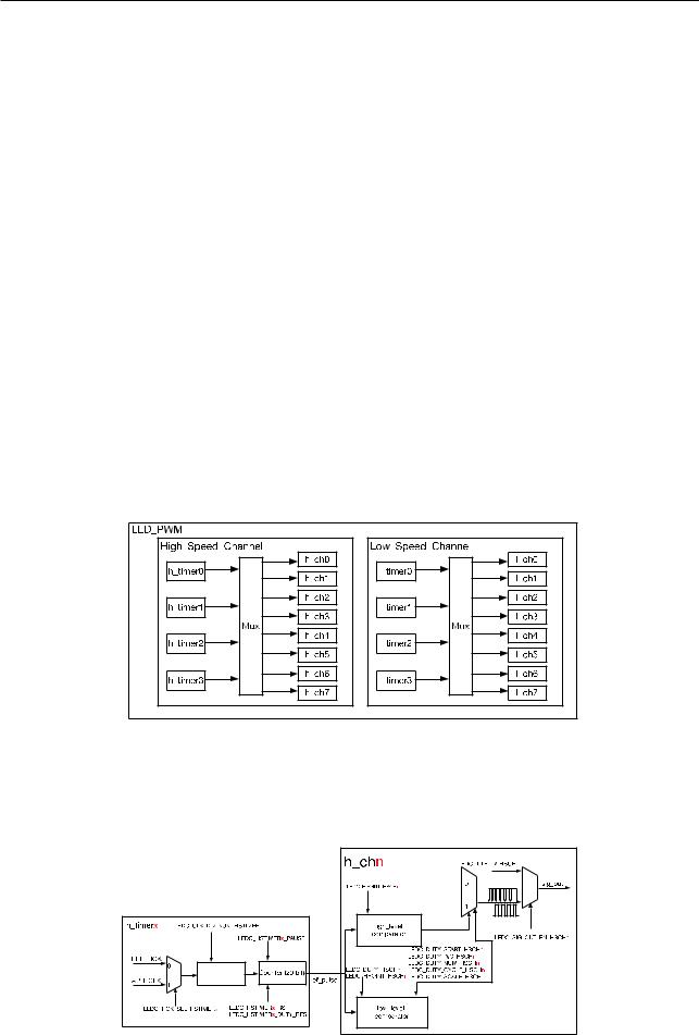
The LED_PWM controller is primarily designed to control the intensity of LEDs, although it can be used to generate PWM signals for other purposes as well. It has 16 channels which can generate independent waveforms that can be used to drive RGB LED devices. For maximum flexibility, the high-speed as well as the low-speed channels can be driven from one of four high-speed/low-speed timers. The PWM controller also has the ability to automatically increase or decrease the duty cycle gradually, allowing for fades without any processor interference. To increase resolution, the LED_PWM controller is also able to dither between two values, when a fractional PWM value is configured.
The LED_PWM controller has eight high-speed and eight low-speed PWM generators. In this document, they will be referred to as hschn and lschn, respectively. These channels can be driven from four timers which will be indicated by h_timerx and l_timerx.
14.2Functional Description
14.2.1 Architecture
Figure 14-1 shows the architecture of the LED_PWM controller. As can be seen in the figure, the LED_PWM controller contains eight high-speed and eight low-speed channels. There are four high-speed clock modules for the high-speed channels, from which one h_timerx can be selected. There are also four low-speed clock modules for the low-speed channels, from which one l_timerx can be selected.
Figure 141. LED_PWM Architecture
Figure 14-2 illustrates a PWM channel with its selected timer; in this instance a high-speed channel and associated high-speed timer.
FRACTIONAL |
DIVIDER (18 BIT) |
Figure 142. LED_PWM Highspeed Channel Diagram
Espressif Systems |
385 |
ESP32 TRM (Version 5.0) |
Submit Documentation Feedback
14 LED PWM Controller (LEDC)
14.2.2 Timers
Divider input clock
... |
... |
... |
... |
... |
... |
... |
... |
Clock pulses |
... |
Clock pulses |
Clock pulses divided |
Clock pulses |
... |
Clock pulses |
Clock pulses divided |
divided by A |
|
divided by A |
by (A+1) |
divided by A |
|
divided by A |
by (A+1) |
B clock pulses divided by (A+1)
... |
... |
... |
|
Clock pulses |
Clock pulses divided |
... |
divided by A |
by (A+1) |
|
|
...
Divider output clock
256 output clock pulses
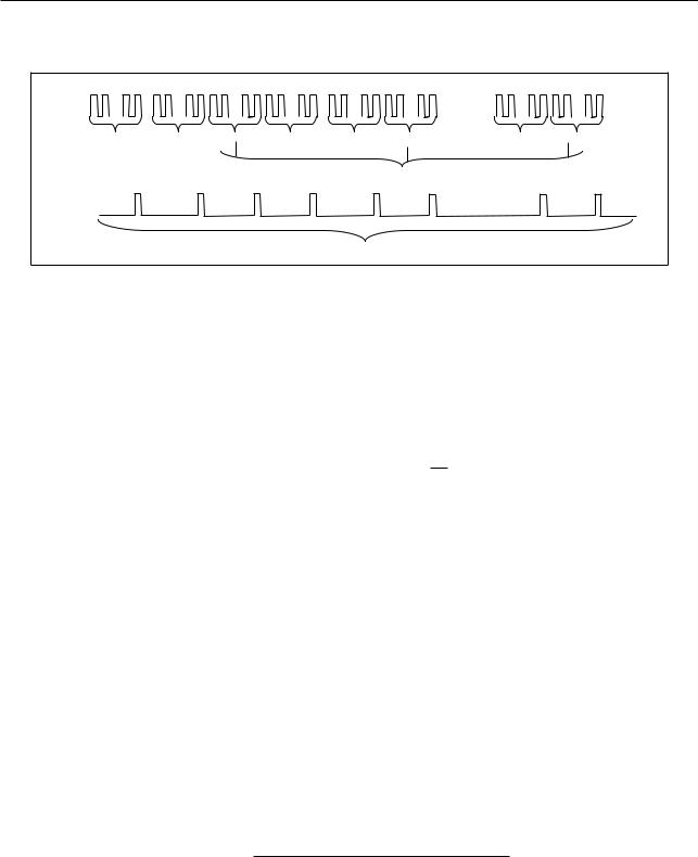
Figure 143. LED_PWM Divider
The clock of each high-speed timer, LEDC_CLKx, has two clock sources: REF_TICK or APB_CLK. For more information on the clock sources, please see Chapter Reset And Clock. The input clock is divided down by a divider first. The division factor is specified by LEDC_CLK_DIV_NUM_HSTIMERx which contains a fixed point number: the highest 10 bits represent the integer portion A, while the lowest eight bits contain the fractional portion B. The effective division factor LEDC_CLK_DIVx is as follows:
LEDC_CLK_DIV x = A + 256B
The division factor ranges from 1 1023.
When the fractional part B is not 0, the input and output clock of the divider is shown as in figure 14-3. Among the 256 output clocks, B of them are divided by (A+1), whereas the remaining (256-B) are divided by A. Output clocks divided by (A+1) are evenly distributed in the total 256 output clocks.
The output clock of the divider is the base clock for the counter which will count up to the value specified in LEDC_HSTIMERx_DUTY_RES. An overflow interrupt will be generated once the counting value reaches
2LEDC_HSTIMERx_DUTY _RES − 1, at which point the counter restarts counting from 0. It is also possible to reset, suspend, and read the values of the counter by software.
The output signal of the timer is the 20-bit value generated by the counter. The cycle period of this signal defines the frequency of the signals of any PWM channels connected to this timer.
The frequency of a PWM generator output signal, sig_outn, depends on the frequency of the timer’s clock source LEDC_CLKx, the division factor of the divider LEDC_CLK_DIVx, as well as the duty resolution (counter width) LEDC_HSTIMERx_DUTY_RES:
fLEDC_CLKx
fsig_outn = LEDC_CLK_DIVx · 2LEDC_HSTIMERx_DUTY_RES
Based on the formula above, the desired duty resolution can be calculated as follows:
LEDC_HSTIMERx_DUTY_RES = log2 |
|
fLEDC_CLKx |
|
fsig_outn · LEDC_CLK_DIVx |
Table 14-1 lists the commonly-used frequencies and their corresponding resolutions.
Espressif Systems |
386 |
ESP32 TRM (Version 5.0) |
Submit Documentation Feedback
14 LED PWM Controller (LEDC)
Table 141. Commonlyused Frequencies and Resolutions
LEDC_CLKx |
PWM Frequency |
Highest Resolution (bit) 1 |
Lowest Resolution (bit) 2 |
APB_CLK (80 MHz) |
1 kHz |
16 |
6 |
|
|
|
|
APB_CLK (80 MHz) |
5 kHz |
13 |
3 |
|
|
|
|
APB_CLK (80 MHz) |
10 kHz |
12 |
2 |
|
|
|
|
RC_FAST_CLK (8 MHz) |
1 kHz |
12 |
2 |
|
|
|
|
RC_FAST_CLK (8 MHz) |
2 kHz |
11 |
1 |
|
|
|
|
REF_TICK (1 MHz) |
1 kHz |
9 |
1 |
|
|
|
|
1The highest resolution is calculated when the clock divisor LEDC_CLK_DIVx is 1. If the highest resolution calculated by the formula is higher than the counter’s width 20 bits, then the highest
resolution should be 20 bits.
2The lowest resolution is calculated when the clock divisor LEDC_CLK_DIVx is 1023 + 255256 . If the lowest resolution calculated by the formula is lower than 0, then the lowest resolution should be
1.
The low-speed timers l_timerx on the low-speed channel differ from the high-speed timers h_timerx in two aspects:
1.Where the high-speed timer clock source can be clocked from REF_TICK or APB_CLK, the low-speed timers are sourced from either REF_TICK or SLOW_CLOCK. The SLOW_CLOCK source can be either APB_CLK (80 MHz) or 8 MHz, and can be selected using LEDC_APB_CLK_SEL.
2.The high-speed counter and divider are glitch-free, which means that if the software modifies the maximum counter or divisor value, the update will come into effect after the next overflow interrupt. In contrast, the low-speed counter and divider will update these values only when LEDC_LSTIMERx_PARA_UP is set.
14.2.3 Channels
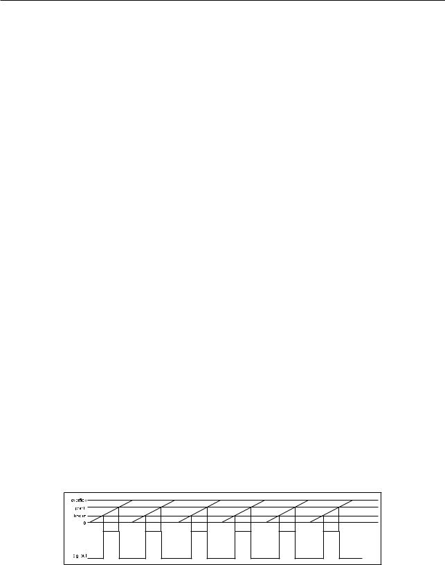
A channel takes the 20-bit value from the counter of the selected high-speed timer and compares it to a set of two values in order to set the channel output. The first value it is compared to is the content of LEDC_HPOINT_HSCHn; if these two match, the output will be latched high. The second value is the sum of LEDC_HPOINT_HSCHn and LEDC_DUTY_HSCHn[24..4]. When this value is reached, the output is latched low. By using these two values, the relative phase and the duty cycle of the PWM output can be set. Figure 14-4 illustrates this.
Figure 144. LED PWM Output Signal Diagram
LEDC_DUTY_HSCHn is a fixed-point register with four fractional bits. As mentioned before, when LEDC_DUTY_ HSCHn[24..4] is used in the PWM calculation directly, LEDC_DUTY_HSCHn[3..0] can be used to dither the output. If this value is non-zero, with a statistical chance of LEDC_DUTY_HSCHn[3..0]/16, the actual PWM pulse will be one cycle longer. This effectively increases the resolution of the PWM generator to 25 bits, but at the cost of a slight jitter in the duty cycle.
Espressif Systems |
387 |
ESP32 TRM (Version 5.0) |
Submit Documentation Feedback