

- •1 System and Memory
- •1.1 Introduction
- •1.2 Features
- •1.3 Functional Description
- •1.3.1 Address Mapping
- •1.3.2 Embedded Memory
- •1.3.3 External Memory
- •1.3.5 Peripherals
- •2 Interrupt Matrix (INTERRUPT)
- •2.1 Overview
- •2.2 Features
- •2.3 Functional Description
- •2.3.1 Peripheral Interrupt Source
- •2.3.2 CPU Interrupt
- •2.3.3 Allocate Peripheral Interrupt Sources to Peripheral Interrupt on CPU
- •2.3.4 CPU NMI Interrupt Mask
- •2.3.5 Query Current Interrupt Status of Peripheral Interrupt Source
- •2.4 Registers
- •3 Reset and Clock
- •3.1 System Reset
- •3.1.1 Introduction
- •3.1.2 Reset Source
- •3.2 System Clock
- •3.2.1 Introduction
- •3.2.3 CPU Clock
- •3.2.4 Peripheral Clock
- •3.2.7 Audio PLL
- •3.3 Register Summary
- •3.4 Registers
- •4.1 Overview
- •4.2 Peripheral Input via GPIO Matrix
- •4.2.1 Summary
- •4.2.2 Functional Description
- •4.2.3 Simple GPIO Input
- •4.3 Peripheral Output via GPIO Matrix
- •4.3.1 Summary
- •4.3.3 Simple GPIO Output
- •4.4 Direct I/O via IO_MUX
- •4.4.1 Summary
- •4.4.2 Functional Description
- •4.5 RTC IO_MUX for Low Power and Analog I/O
- •4.5.1 Summary
- •4.5.2 Analog Function Description
- •4.7 Pad Hold Feature
- •4.8 I/O Pad Power Supplies
- •4.8.1 VDD_SDIO Power Domain
- •4.9 Peripheral Signal List
- •4.10 IO_MUX Pad List
- •4.11 RTC_MUX Pin List
- •4.12 Register Summary
- •4.12.1 GPIO Matrix Register Summary
- •4.12.2 IO MUX Register Summary
- •4.12.3 RTC IO MUX Register Summary
- •4.13 Registers
- •4.13.1 GPIO Matrix Registers
- •4.13.2 IO MUX Registers
- •4.13.3 RTC IO MUX Registers
- •5 DPort Registers
- •5.1 Introduction
- •5.2 Features
- •5.3 Functional Description
- •5.3.1 System and Memory Register
- •5.3.2 Reset and Clock Registers
- •5.3.3 Interrupt Matrix Register
- •5.3.4 DMA Registers
- •5.3.5 MPU/MMU Registers
- •5.3.7 Peripheral Clock Gating and Reset
- •5.4 Register Summary
- •5.5 Registers
- •6 DMA Controller (DMA)
- •6.1 Overview
- •6.2 Features
- •6.3 Functional Description
- •6.3.1 DMA Engine Architecture
- •6.3.2 Linked List
- •6.4 UART DMA (UDMA)
- •7 SPI Controller (SPI)
- •7.1 Overview
- •7.5 Parallel QSPI
- •7.5.1 Communication Format of Parallel QSPI
- •7.6.1 SPI Interrupts
- •7.6.2 DMA Interrupts
- •7.7 Register Summary
- •7.8 Registers
- •8 SDIO Slave Controller
- •8.1 Overview
- •8.2 Features
- •8.3 Functional Description
- •8.3.1 SDIO Slave Block Diagram
- •8.3.3 Register Access
- •8.3.6 SDIO Bus Timing
- •8.3.7 Interrupt
- •8.4 Register Summary
- •8.5 SLC Registers
- •8.6 SLC Host Registers
- •8.7 HINF Registers
- •9 SD/MMC Host Controller
- •9.1 Overview
- •9.2 Features
- •9.3 SD/MMC External Interface Signals
- •9.4 Functional Description
- •9.4.1 SD/MMC Host Controller Architecture
- •9.4.2 Command Path
- •9.4.3 Data Path
- •9.5 Software Restrictions for Proper CIU Operation
- •9.6 RAM for Receiving and Sending Data
- •9.6.1 Transmit RAM Module
- •9.6.2 Receive RAM Module
- •9.8 The Structure of a Linked List
- •9.9 Initialization
- •9.9.1 DMAC Initialization
- •9.9.2 DMAC Transmission Initialization
- •9.9.3 DMAC Reception Initialization
- •9.11 Interrupt
- •9.12 Register Summary
- •9.13 Registers
- •10 Ethernet Media Access Controller (MAC)
- •10.1 Overview
- •10.2 EMAC_CORE
- •10.2.1 Transmit Operation
- •10.2.2 Receive Operation
- •10.3 MAC Interrupt Controller
- •10.4 MAC Address Filtering
- •10.4.1 Unicast Destination Address Filtering
- •10.4.2 Multicast Destination Address Filtering
- •10.4.3 Broadcast Address Filtering
- •10.4.4 Unicast Source Address Filtering
- •10.4.5 Inverse Filtering Operation
- •10.4.6 Good Transmitted Frames and Received Frames
- •10.5 EMAC_MTL (MAC Transaction Layer)
- •10.6 PHY Interface
- •10.6.1 MII (Media Independent Interface)
- •10.6.3 Station Management Agent (SMA) Interface
- •10.6.4 RMII Timing
- •10.7 Ethernet DMA Features
- •10.8 Linked List Descriptors
- •10.8.1 Transmit Descriptors
- •10.8.2 Receive Descriptors
- •10.9 Register Summary
- •10.10 Registers
- •11 I2C Controller (I2C)
- •11.1 Overview
- •11.2 Features
- •11.3 Functional Description
- •11.3.1 Introduction
- •11.3.2 Architecture
- •11.3.3 I2C Bus Timing
- •11.3.7 Interrupts
- •11.4 Register Summary
- •11.5 Registers
- •12 I2S Controller (I2S)
- •12.1 Overview
- •12.2 Features
- •12.3 The Clock of I2S Module
- •12.4 I2S Mode
- •12.4.1 Supported Audio Standards
- •12.4.2 Module Reset
- •12.4.3 FIFO Operation
- •12.4.5 Receiving Data
- •12.5.1 LCD Master Transmitting Mode
- •12.5.2 Camera Slave Receiving Mode
- •12.5.3 ADC/DAC mode
- •12.6 I2S Interrupts
- •12.6.1 FIFO Interrupts
- •12.6.2 DMA Interrupts
- •12.7 Register Summary
- •12.8 Registers
- •13 UART Controller (UART)
- •13.1 Overview
- •13.2 UART Features
- •13.3 Functional Description
- •13.3.1 Introduction
- •13.3.3 UART RAM
- •13.3.5 UART Data Frame
- •13.3.7 Flow Control
- •13.3.8 UART DMA
- •13.3.9 UART Interrupts
- •13.3.10 UHCI Interrupts
- •13.4 Register Summary
- •13.4.1 UART Register Summary
- •13.5 Registers
- •13.5.1 UART Registers
- •13.5.2 UHCI Registers
- •14 LED PWM Controller (LEDC)
- •14.1 Introduction
- •14.2 Functional Description
- •14.2.1 Architecture
- •14.2.3 Channels
- •14.2.4 Interrupts
- •14.3 Register Summary
- •14.4 Registers
- •15 Remote Control Peripheral (RMT)
- •15.1 Introduction
- •15.2 Functional Description
- •15.2.1 RMT Architecture
- •15.2.3 Clock
- •15.2.4 Transmitter
- •15.2.5 Receiver
- •15.2.6 Interrupts
- •15.3 Register Summary
- •15.4 Registers
- •16 Motor Control PWM (PWM)
- •16.1 Introduction
- •16.2 Features
- •16.3 Submodules
- •16.3.1 Overview
- •16.3.2 PWM Timer Submodule
- •16.3.3 PWM Operator Submodule
- •16.3.4 Capture Submodule
- •16.4 Register Summary
- •16.5 Registers
- •17 Pulse Count Controller (PCNT)
- •17.1 Overview
- •17.2 Functional Description
- •17.2.1 Architecture
- •17.2.2 Counter Channel Inputs
- •17.2.3 Watchpoints
- •17.2.4 Examples
- •17.2.5 Interrupts
- •18 Timer Group (TIMG)
- •18.1 Introduction
- •18.2 Functional Description
- •18.2.2 64-bit Time-base Counter
- •18.2.3 Alarm Generation
- •18.2.4 MWDT
- •18.2.5 Interrupts
- •18.3 Register Summary
- •18.4 Registers
- •19 Watchdog Timers (WDT)
- •19.1 Introduction
- •19.2 Features
- •19.3 Functional Description
- •19.3.1 Clock
- •20 eFuse Controller
- •20.1 Introduction
- •20.2 Features
- •20.3 Functional Description
- •20.3.1 Structure
- •20.3.3 Software Reading of System Parameters
- •20.3.4 The Use of System Parameters by Hardware Modules
- •20.3.5 Interrupts
- •20.4 Register Summary
- •20.5 Registers
- •21 Two-wire Automotive Interface (TWAI)
- •21.1 Overview
- •21.2 Features
- •21.3 Functional Protocol
- •21.3.1 TWAI Properties
- •21.3.2 TWAI Messages
- •21.3.3 TWAI Errors
- •21.3.4 TWAI Bit Timing
- •21.4 Architectural Overview
- •21.4.1 Registers Block
- •21.4.2 Bit Stream Processor
- •21.4.3 Error Management Logic
- •21.4.4 Bit Timing Logic
- •21.4.5 Acceptance Filter
- •21.5 Functional Description
- •21.5.1 Modes
- •21.5.2 Bit Timing
- •21.5.3 Interrupt Management
- •21.5.4 Transmit and Receive Buffers
- •21.5.5 Receive FIFO and Data Overruns
- •21.5.6 Acceptance Filter
- •21.5.8 Error Code Capture
- •21.5.9 Arbitration Lost Capture
- •21.6 Register Summary
- •21.7 Registers
- •22 AES Accelerator (AES)
- •22.1 Introduction
- •22.2 Features
- •22.3 Functional Description
- •22.3.1 AES Algorithm Operations
- •22.3.2 Key, Plaintext and Ciphertext
- •22.3.3 Endianness
- •22.3.4 Encryption and Decryption Operations
- •22.3.5 Speed
- •22.4 Register Summary
- •22.5 Registers
- •23 SHA Accelerator (SHA)
- •23.1 Introduction
- •23.2 Features
- •23.3 Functional Description
- •23.3.1 Padding and Parsing the Message
- •23.3.2 Message Digest
- •23.3.3 Hash Operation
- •23.3.4 Speed
- •23.4 Register Summary
- •23.5 Registers
- •24 RSA Accelerator (RSA)
- •24.1 Introduction
- •24.2 Features
- •24.3 Functional Description
- •24.3.1 Initialization
- •24.3.2 Large Number Modular Exponentiation
- •24.3.4 Large Number Multiplication
- •24.4 Register Summary
- •24.5 Registers
- •25 Random Number Generator (RNG)
- •25.1 Introduction
- •25.2 Feature
- •25.3 Functional Description
- •25.5 Register Summary
- •25.6 Register
- •26 External Memory Encryption and Decryption (FLASH)
- •26.1 Overview
- •26.2 Features
- •26.3 Functional Description
- •26.3.1 Key Generator
- •26.3.2 Flash Encryption Block
- •26.3.3 Flash Decryption Block
- •26.4 Register Summary
- •26.5 Register
- •27 Memory Management and Protection Units (MMU, MPU)
- •27.1 Introduction
- •27.2 Features
- •27.3 Functional Description
- •27.3.1 PID Controller
- •28 Process ID Controller (PID)
- •28.1 Overview
- •28.2 Features
- •28.3 Functional Description
- •28.3.1 Interrupt Identification
- •28.3.2 Information Recording
- •28.3.3 Proactive Process Switching
- •28.4 Register Summary
- •28.5 Registers
- •29 On-Chip Sensors and Analog Signal Processing
- •29.1 Introduction
- •29.2 Capacitive Touch Sensor
- •29.2.1 Introduction
- •29.2.2 Features
- •29.2.3 Available GPIOs
- •29.2.4 Functional Description
- •29.2.5 Touch FSM
- •29.3.1 Introduction
- •29.3.2 Features
- •29.3.3 Outline of Function
- •29.3.4 RTC SAR ADC Controllers
- •29.3.5 DIG SAR ADC Controllers
- •29.4.1 Introduction
- •29.4.2 Features
- •29.4.4 Cosine Waveform Generator
- •29.5 Register Summary
- •29.5.1 Sensors
- •29.5.2 Advanced Peripheral Bus
- •29.6 Registers
- •29.6.1 Sensors
- •29.6.2 Advanced Peripheral Bus
- •30 ULP Coprocessor (ULP)
- •30.1 Introduction
- •30.2 Features
- •30.4 Instruction Set
- •30.4.2 ST – Store Data in Memory
- •30.4.3 LD – Load Data from Memory
- •30.4.4 JUMP – Jump to an Absolute Address
- •30.4.5 JUMPR – Jump to a Relative Offset (Conditional upon R0)
- •30.4.7 HALT – End the Program
- •30.4.8 WAKE – Wake up the Chip
- •30.4.10 WAIT – Wait for a Number of Cycles
- •30.4.12 I2C_RD/I2C_WR – Read/Write I²C
- •30.4.13 REG_RD – Read from Peripheral Register
- •30.5 ULP Program Execution
- •30.6 RTC_I2C Controller
- •30.6.1 Configuring RTC_I2C
- •30.6.2 Using RTC_I2C
- •30.7 Register Summary
- •30.7.1 SENS_ULP Address Space
- •30.7.2 RTC_I2C Address Space
- •30.8 Registers
- •30.8.1 SENS_ULP Address Space
- •30.8.2 RTC_I2C Address Space
- •31 Low-Power Management (RTC_CNTL)
- •31.1 Introduction
- •31.2 Features
- •31.3 Functional Description
- •31.3.2 Digital Core Voltage Regulator
- •31.3.4 Flash Voltage Regulator
- •31.3.5 Brownout Detector
- •31.3.6 RTC Module
- •31.3.9 Predefined Power Modes
- •31.3.10 Wakeup Source
- •31.3.12 RTC Timer
- •31.3.13 RTC Boot
- •31.4 Register Summary
- •31.5 Registers
- •Glossary
- •Abbreviations for Peripherals
- •Abbreviations for Registers
- •Revision History
12 I2S Controller (I2S)
Table 12-7 shows the configuration of the I2S_RX_PDM_SINC_DSR_16_EN bit whose PCM signal frequency remains 48 KHz at different PDM signal frequencies.
Table 127. Downsampling Configuration
PDM freq (KHz) |
I2S_RX_PDM_SINC_DSR_16_EN |
PCM freq (KHz) |
|
fpcm×128 |
1 |
fpcm |
|
fpcm×64 |
0 |
||
|
12.5CameraLCD Controller
There are three operational modes in the LCD mode of ESP32 I2S:
•LCD master transmitting mode
•Camera slave receiving mode
•ADC/DAC mode
The clock configuration of the LCD master transmitting mode is identical to I2S’ clock configuration. In the LCD mode, the frequency of WS is half of fBCK.
In the ADC/DAC mode, use PLL_F160M_CLK as the clock source.
12.5.1 LCD Master Transmitting Mode
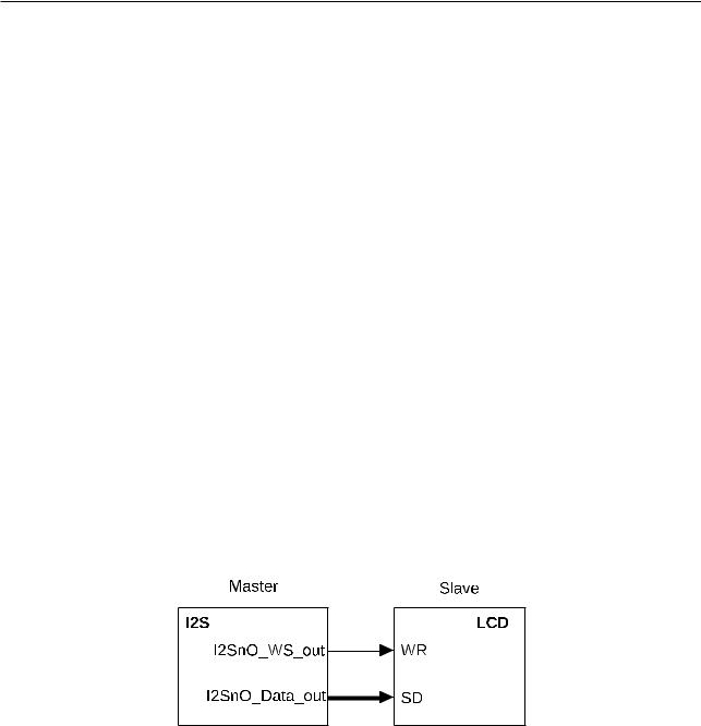
As is shown in Figure 12-13, the WR signal of LCD connects to the WS signal of I2S. The LCD data bus width is 24 bits.
Figure 1213. LCD Master Transmitting Mode
The I2S_LCD_EN bit of register I2S_CONF2_REG needs to be set and the I2S_TX_SLAVE_MOD bit of register I2S_CONF_REG needs to be cleared, in order to configure I2S to the LCD master transmitting mode. Meanwhile, data should be sent under the correct mode, according to the I2S_TX_CHAN_MOD[2:0] bit of register I2S_CONF_CHAN_REG and the I2S_TX_FIFO_MOD[2:0] bit of register I2S_FIFO_CONF_REG. The WS signal needs to be inverted when it is routed through the GPIO Matrix. For details, please refer to the chapter about IO_MUX and the GPIO Matrix. The I2S_LCD_TX_SDX2_EN bit and the I2S_LCD_TX_WRX2_EN bit of register I2S_CONF2_REG should be set to the LCD master transmitting mode, so that both the data bus and WR signal work in the appropriate mode.
Espressif Systems |
318 |
ESP32 TRM (Version 5.0) |
Submit Documentation Feedback
12 I2S Controller (I2S)
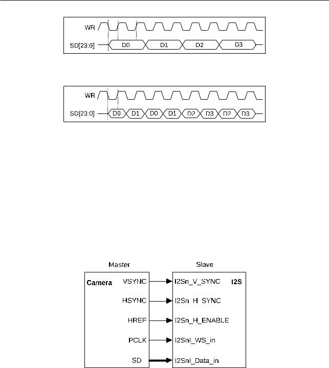
Figure 1214. LCD Master Transmitting Data Frame, Form 1
Figure 1215. LCD Master Transmitting Data Frame, Form 2
As is shown in Figure 12-14 and Figure 12-15, the I2S_LCD_TX_WRX2_EN bit should be set to 1 and the I2S_LCD_TX_SDX2_EN bit should be set to 0 in the data frame, form 1. Both I2S_LCD_TX_SDX2_EN bit and I2S_LCD_TX_WRX2_EN bit are set to 1 in the data frame, form 2.
12.5.2 Camera Slave Receiving Mode
ESP32 I2S supports a camera slave mode for high-speed data transfer from external camera modules. As shown in Figure 12-16, in this mode, I2S is set to slave receiving mode. Besides the 16-channel data signal bus I2SnI_Data_in, there are other signals, such as I2Sn_H_SYNC, I2Sn_V_SYNC and I2Sn_H_ENABLE.
The PCLK in the Camera module connects to I2SnI_WS_in in the I2S module, as Figure 12-16 shows.
Figure 1216. Camera Slave Receiving Mode
When I2S is in the camera slave receiving mode, and when I2Sn_H_SYNC, I2S_V_SYNC and I2S_H_REF are held high, the master starts transmitting data, that is,
transmission_start = (I2Sn_H_SY NC == 1)&&(I2Sn_V _SY NC == 1)&&(I2Sn_H_ENABLE == 1)
Thus, during data transmission, these three signals should be kept at a high level. For example, if the I2Sn_V_SYNC signal of a camera is at low level during data transmission, it will be inverted when routed to the I2S module. ESP32 supports signal inversion through the GPIO matrix. For details, please refer to the chapter about IO_MUX and the GPIO Matrix.
In order to make I2S work in camera mode, the I2S_LCD_EN bit and the I2S_CAMERA_EN bit of register I2S_CONF2 _REG are set to 1, the I2S_RX_SLAVE_MOD bit of register I2S_CONF_REG is set to 1, the I2S_RX_MSB_RIGHT
Espressif Systems |
319 |
ESP32 TRM (Version 5.0) |
Submit Documentation Feedback
12 I2S Controller (I2S)
bit and the I2S_RX_RIGHT_FIRST bit of I2S_CONF_REG are set to 0. Thus, I2S works in the LCD slave receiving mode. At the same time, in order to use the correct mode to receive data, both the I2S_RX_CHAN_MOD[2:0] bit of register I2S_CONF_CHAN_REG and the I2S_RX_FIFO_MOD[2:0] bit of register I2S_FIFO_CONF_REG are set to 1.
12.5.3 ADC/DAC mode
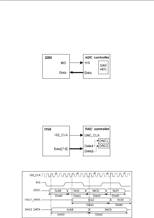
In LCD mode, ESP32’s ADC and DAC can receive data. When the I2S0 module connects to the on-chip ADC, the I2S0 module should be set to master receiving mode. Figure 12-17 shows the signal connection between the I2S0 module and the ADC.
Figure 1217. ADC Interface of I2S0
Firstly, the I2S_LCD_EN bit of register I2S_CONF2_REG is set to 1, and the I2S_RX_SLAVE_MOD bit of register I2S_CONF_REG is set to 0, so that the I2S0 module works in LCD master receiving mode, and the I2S0 module clock is configured such that the WS signal of I2S0 outputs an appropriate frequency. Then, the SYSCON_SAR ADC_DATA_TO_I2S bit of register SYSCON_APB_SARADC_CTRL_REG is set to 1. Enable I2S to receive data after configuring the relevant registers of SARADC. For details, please refer to Chapter On-Chip Sensors and Analog Signal Processing.
Figure 1218. DAC Interface of I2S
Figure 1219. Data Input by I2S DAC Interface
The I2S0 module should be configured to master transmitting mode when it connects to the on-chip DAC. Figure
Espressif Systems |
320 |
ESP32 TRM (Version 5.0) |
Submit Documentation Feedback