

- •1 System and Memory
- •1.1 Introduction
- •1.2 Features
- •1.3 Functional Description
- •1.3.1 Address Mapping
- •1.3.2 Embedded Memory
- •1.3.3 External Memory
- •1.3.5 Peripherals
- •2 Interrupt Matrix (INTERRUPT)
- •2.1 Overview
- •2.2 Features
- •2.3 Functional Description
- •2.3.1 Peripheral Interrupt Source
- •2.3.2 CPU Interrupt
- •2.3.3 Allocate Peripheral Interrupt Sources to Peripheral Interrupt on CPU
- •2.3.4 CPU NMI Interrupt Mask
- •2.3.5 Query Current Interrupt Status of Peripheral Interrupt Source
- •2.4 Registers
- •3 Reset and Clock
- •3.1 System Reset
- •3.1.1 Introduction
- •3.1.2 Reset Source
- •3.2 System Clock
- •3.2.1 Introduction
- •3.2.3 CPU Clock
- •3.2.4 Peripheral Clock
- •3.2.7 Audio PLL
- •3.3 Register Summary
- •3.4 Registers
- •4.1 Overview
- •4.2 Peripheral Input via GPIO Matrix
- •4.2.1 Summary
- •4.2.2 Functional Description
- •4.2.3 Simple GPIO Input
- •4.3 Peripheral Output via GPIO Matrix
- •4.3.1 Summary
- •4.3.3 Simple GPIO Output
- •4.4 Direct I/O via IO_MUX
- •4.4.1 Summary
- •4.4.2 Functional Description
- •4.5 RTC IO_MUX for Low Power and Analog I/O
- •4.5.1 Summary
- •4.5.2 Analog Function Description
- •4.7 Pad Hold Feature
- •4.8 I/O Pad Power Supplies
- •4.8.1 VDD_SDIO Power Domain
- •4.9 Peripheral Signal List
- •4.10 IO_MUX Pad List
- •4.11 RTC_MUX Pin List
- •4.12 Register Summary
- •4.12.1 GPIO Matrix Register Summary
- •4.12.2 IO MUX Register Summary
- •4.12.3 RTC IO MUX Register Summary
- •4.13 Registers
- •4.13.1 GPIO Matrix Registers
- •4.13.2 IO MUX Registers
- •4.13.3 RTC IO MUX Registers
- •5 DPort Registers
- •5.1 Introduction
- •5.2 Features
- •5.3 Functional Description
- •5.3.1 System and Memory Register
- •5.3.2 Reset and Clock Registers
- •5.3.3 Interrupt Matrix Register
- •5.3.4 DMA Registers
- •5.3.5 MPU/MMU Registers
- •5.3.7 Peripheral Clock Gating and Reset
- •5.4 Register Summary
- •5.5 Registers
- •6 DMA Controller (DMA)
- •6.1 Overview
- •6.2 Features
- •6.3 Functional Description
- •6.3.1 DMA Engine Architecture
- •6.3.2 Linked List
- •6.4 UART DMA (UDMA)
- •7 SPI Controller (SPI)
- •7.1 Overview
- •7.5 Parallel QSPI
- •7.5.1 Communication Format of Parallel QSPI
- •7.6.1 SPI Interrupts
- •7.6.2 DMA Interrupts
- •7.7 Register Summary
- •7.8 Registers
- •8 SDIO Slave Controller
- •8.1 Overview
- •8.2 Features
- •8.3 Functional Description
- •8.3.1 SDIO Slave Block Diagram
- •8.3.3 Register Access
- •8.3.6 SDIO Bus Timing
- •8.3.7 Interrupt
- •8.4 Register Summary
- •8.5 SLC Registers
- •8.6 SLC Host Registers
- •8.7 HINF Registers
- •9 SD/MMC Host Controller
- •9.1 Overview
- •9.2 Features
- •9.3 SD/MMC External Interface Signals
- •9.4 Functional Description
- •9.4.1 SD/MMC Host Controller Architecture
- •9.4.2 Command Path
- •9.4.3 Data Path
- •9.5 Software Restrictions for Proper CIU Operation
- •9.6 RAM for Receiving and Sending Data
- •9.6.1 Transmit RAM Module
- •9.6.2 Receive RAM Module
- •9.8 The Structure of a Linked List
- •9.9 Initialization
- •9.9.1 DMAC Initialization
- •9.9.2 DMAC Transmission Initialization
- •9.9.3 DMAC Reception Initialization
- •9.11 Interrupt
- •9.12 Register Summary
- •9.13 Registers
- •10 Ethernet Media Access Controller (MAC)
- •10.1 Overview
- •10.2 EMAC_CORE
- •10.2.1 Transmit Operation
- •10.2.2 Receive Operation
- •10.3 MAC Interrupt Controller
- •10.4 MAC Address Filtering
- •10.4.1 Unicast Destination Address Filtering
- •10.4.2 Multicast Destination Address Filtering
- •10.4.3 Broadcast Address Filtering
- •10.4.4 Unicast Source Address Filtering
- •10.4.5 Inverse Filtering Operation
- •10.4.6 Good Transmitted Frames and Received Frames
- •10.5 EMAC_MTL (MAC Transaction Layer)
- •10.6 PHY Interface
- •10.6.1 MII (Media Independent Interface)
- •10.6.3 Station Management Agent (SMA) Interface
- •10.6.4 RMII Timing
- •10.7 Ethernet DMA Features
- •10.8 Linked List Descriptors
- •10.8.1 Transmit Descriptors
- •10.8.2 Receive Descriptors
- •10.9 Register Summary
- •10.10 Registers
- •11 I2C Controller (I2C)
- •11.1 Overview
- •11.2 Features
- •11.3 Functional Description
- •11.3.1 Introduction
- •11.3.2 Architecture
- •11.3.3 I2C Bus Timing
- •11.3.7 Interrupts
- •11.4 Register Summary
- •11.5 Registers
- •12 I2S Controller (I2S)
- •12.1 Overview
- •12.2 Features
- •12.3 The Clock of I2S Module
- •12.4 I2S Mode
- •12.4.1 Supported Audio Standards
- •12.4.2 Module Reset
- •12.4.3 FIFO Operation
- •12.4.5 Receiving Data
- •12.5.1 LCD Master Transmitting Mode
- •12.5.2 Camera Slave Receiving Mode
- •12.5.3 ADC/DAC mode
- •12.6 I2S Interrupts
- •12.6.1 FIFO Interrupts
- •12.6.2 DMA Interrupts
- •12.7 Register Summary
- •12.8 Registers
- •13 UART Controller (UART)
- •13.1 Overview
- •13.2 UART Features
- •13.3 Functional Description
- •13.3.1 Introduction
- •13.3.3 UART RAM
- •13.3.5 UART Data Frame
- •13.3.7 Flow Control
- •13.3.8 UART DMA
- •13.3.9 UART Interrupts
- •13.3.10 UHCI Interrupts
- •13.4 Register Summary
- •13.4.1 UART Register Summary
- •13.5 Registers
- •13.5.1 UART Registers
- •13.5.2 UHCI Registers
- •14 LED PWM Controller (LEDC)
- •14.1 Introduction
- •14.2 Functional Description
- •14.2.1 Architecture
- •14.2.3 Channels
- •14.2.4 Interrupts
- •14.3 Register Summary
- •14.4 Registers
- •15 Remote Control Peripheral (RMT)
- •15.1 Introduction
- •15.2 Functional Description
- •15.2.1 RMT Architecture
- •15.2.3 Clock
- •15.2.4 Transmitter
- •15.2.5 Receiver
- •15.2.6 Interrupts
- •15.3 Register Summary
- •15.4 Registers
- •16 Motor Control PWM (PWM)
- •16.1 Introduction
- •16.2 Features
- •16.3 Submodules
- •16.3.1 Overview
- •16.3.2 PWM Timer Submodule
- •16.3.3 PWM Operator Submodule
- •16.3.4 Capture Submodule
- •16.4 Register Summary
- •16.5 Registers
- •17 Pulse Count Controller (PCNT)
- •17.1 Overview
- •17.2 Functional Description
- •17.2.1 Architecture
- •17.2.2 Counter Channel Inputs
- •17.2.3 Watchpoints
- •17.2.4 Examples
- •17.2.5 Interrupts
- •18 Timer Group (TIMG)
- •18.1 Introduction
- •18.2 Functional Description
- •18.2.2 64-bit Time-base Counter
- •18.2.3 Alarm Generation
- •18.2.4 MWDT
- •18.2.5 Interrupts
- •18.3 Register Summary
- •18.4 Registers
- •19 Watchdog Timers (WDT)
- •19.1 Introduction
- •19.2 Features
- •19.3 Functional Description
- •19.3.1 Clock
- •20 eFuse Controller
- •20.1 Introduction
- •20.2 Features
- •20.3 Functional Description
- •20.3.1 Structure
- •20.3.3 Software Reading of System Parameters
- •20.3.4 The Use of System Parameters by Hardware Modules
- •20.3.5 Interrupts
- •20.4 Register Summary
- •20.5 Registers
- •21 Two-wire Automotive Interface (TWAI)
- •21.1 Overview
- •21.2 Features
- •21.3 Functional Protocol
- •21.3.1 TWAI Properties
- •21.3.2 TWAI Messages
- •21.3.3 TWAI Errors
- •21.3.4 TWAI Bit Timing
- •21.4 Architectural Overview
- •21.4.1 Registers Block
- •21.4.2 Bit Stream Processor
- •21.4.3 Error Management Logic
- •21.4.4 Bit Timing Logic
- •21.4.5 Acceptance Filter
- •21.5 Functional Description
- •21.5.1 Modes
- •21.5.2 Bit Timing
- •21.5.3 Interrupt Management
- •21.5.4 Transmit and Receive Buffers
- •21.5.5 Receive FIFO and Data Overruns
- •21.5.6 Acceptance Filter
- •21.5.8 Error Code Capture
- •21.5.9 Arbitration Lost Capture
- •21.6 Register Summary
- •21.7 Registers
- •22 AES Accelerator (AES)
- •22.1 Introduction
- •22.2 Features
- •22.3 Functional Description
- •22.3.1 AES Algorithm Operations
- •22.3.2 Key, Plaintext and Ciphertext
- •22.3.3 Endianness
- •22.3.4 Encryption and Decryption Operations
- •22.3.5 Speed
- •22.4 Register Summary
- •22.5 Registers
- •23 SHA Accelerator (SHA)
- •23.1 Introduction
- •23.2 Features
- •23.3 Functional Description
- •23.3.1 Padding and Parsing the Message
- •23.3.2 Message Digest
- •23.3.3 Hash Operation
- •23.3.4 Speed
- •23.4 Register Summary
- •23.5 Registers
- •24 RSA Accelerator (RSA)
- •24.1 Introduction
- •24.2 Features
- •24.3 Functional Description
- •24.3.1 Initialization
- •24.3.2 Large Number Modular Exponentiation
- •24.3.4 Large Number Multiplication
- •24.4 Register Summary
- •24.5 Registers
- •25 Random Number Generator (RNG)
- •25.1 Introduction
- •25.2 Feature
- •25.3 Functional Description
- •25.5 Register Summary
- •25.6 Register
- •26 External Memory Encryption and Decryption (FLASH)
- •26.1 Overview
- •26.2 Features
- •26.3 Functional Description
- •26.3.1 Key Generator
- •26.3.2 Flash Encryption Block
- •26.3.3 Flash Decryption Block
- •26.4 Register Summary
- •26.5 Register
- •27 Memory Management and Protection Units (MMU, MPU)
- •27.1 Introduction
- •27.2 Features
- •27.3 Functional Description
- •27.3.1 PID Controller
- •28 Process ID Controller (PID)
- •28.1 Overview
- •28.2 Features
- •28.3 Functional Description
- •28.3.1 Interrupt Identification
- •28.3.2 Information Recording
- •28.3.3 Proactive Process Switching
- •28.4 Register Summary
- •28.5 Registers
- •29 On-Chip Sensors and Analog Signal Processing
- •29.1 Introduction
- •29.2 Capacitive Touch Sensor
- •29.2.1 Introduction
- •29.2.2 Features
- •29.2.3 Available GPIOs
- •29.2.4 Functional Description
- •29.2.5 Touch FSM
- •29.3.1 Introduction
- •29.3.2 Features
- •29.3.3 Outline of Function
- •29.3.4 RTC SAR ADC Controllers
- •29.3.5 DIG SAR ADC Controllers
- •29.4.1 Introduction
- •29.4.2 Features
- •29.4.4 Cosine Waveform Generator
- •29.5 Register Summary
- •29.5.1 Sensors
- •29.5.2 Advanced Peripheral Bus
- •29.6 Registers
- •29.6.1 Sensors
- •29.6.2 Advanced Peripheral Bus
- •30 ULP Coprocessor (ULP)
- •30.1 Introduction
- •30.2 Features
- •30.4 Instruction Set
- •30.4.2 ST – Store Data in Memory
- •30.4.3 LD – Load Data from Memory
- •30.4.4 JUMP – Jump to an Absolute Address
- •30.4.5 JUMPR – Jump to a Relative Offset (Conditional upon R0)
- •30.4.7 HALT – End the Program
- •30.4.8 WAKE – Wake up the Chip
- •30.4.10 WAIT – Wait for a Number of Cycles
- •30.4.12 I2C_RD/I2C_WR – Read/Write I²C
- •30.4.13 REG_RD – Read from Peripheral Register
- •30.5 ULP Program Execution
- •30.6 RTC_I2C Controller
- •30.6.1 Configuring RTC_I2C
- •30.6.2 Using RTC_I2C
- •30.7 Register Summary
- •30.7.1 SENS_ULP Address Space
- •30.7.2 RTC_I2C Address Space
- •30.8 Registers
- •30.8.1 SENS_ULP Address Space
- •30.8.2 RTC_I2C Address Space
- •31 Low-Power Management (RTC_CNTL)
- •31.1 Introduction
- •31.2 Features
- •31.3 Functional Description
- •31.3.2 Digital Core Voltage Regulator
- •31.3.4 Flash Voltage Regulator
- •31.3.5 Brownout Detector
- •31.3.6 RTC Module
- •31.3.9 Predefined Power Modes
- •31.3.10 Wakeup Source
- •31.3.12 RTC Timer
- •31.3.13 RTC Boot
- •31.4 Register Summary
- •31.5 Registers
- •Glossary
- •Abbreviations for Peripherals
- •Abbreviations for Registers
- •Revision History
12 I2S Controller (I2S)
In master transmitting mode, ”M”, whose value is >=2, is the I2S_TX_BCK_DIV_NUM[5:0] bit of register I2S_SAMPLE _RATE_CONF_REG. In master receiving mode, ”M” is the I2S_RX_BCK_DIV_NUM[5:0] bit of register I2S_SAMPLE _RATE_CONF_REG.
12.4I2S Mode
The ESP32 I2S module integrates an A-law compression/decompression module to enable compression/decompression of the received audio data. The RX_PCM_BYPASS bit and the TX_PCM_BYPASS bit of register I2S_CONF1_REG should be cleared when using the A-law compression/decompression module.
12.4.1 Supported Audio Standards
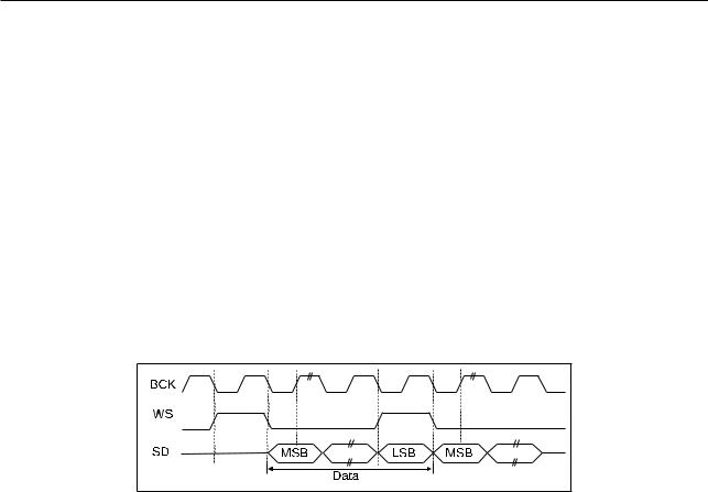
In the I2S bus, BCK is the serial clock, WS is the left- /right-channel selection signal (also called word select signal), and SD is the serial data signal for transmitting/receiving digital audio data. WS and SD signals in the I2S module change on the falling edge of BCK, while the SD signal can be sampled on the rising edge of BCK. If the I2S_RX_RIGHT_FIRST bit and the I2S_TX_RIGHT_FIRST bit of register I2S_CONF_REG are set to 1, the I2S module is configured to receive and transmit right-channel data first. Otherwise, the I2S module receives and transmits left-channel data first.
12.4.1.1 Philips Standard
Figure 123. Philips Standard
As is shown in Figure 12-3, the Philips I2S bus specifications require that the WS signal starts to change one BCK clock cycle earlier than the SD signal on BCK falling edge, which means the WS signal becomes valid one clock cycle before the first bit of data transfer on the current channel, and changes one clock cycle earlier than the end of data transfer on the current channel. The SD signal line transmits the most significant bit of audio data first. If the I2S_RX_MSB_SHIFT bit and the I2S_TX_MSB_SHIFT bit of register I2S_CONF_REG are set to 1, respectively, the I2S module will use the Philips standard when receiving and transmitting data.
12.4.1.2 MSB Alignment Standard
Figure 124. MSB Alignment Standard
Espressif Systems |
311 |
ESP32 TRM (Version 5.0) |
Submit Documentation Feedback
12 I2S Controller (I2S)
The MSB alignment standard is shown in Figure 12-4. WS and SD signals both change simultaneously on the falling edge of BCK under the MSB alignment standard. The WS signal continues until the end of the current channel-data transmission, and the SD signal line transmits the most significant bit of audio data first. If the I2S_RX_MSB_SHIFT and I2S_TX_MSB_SHIFT bits of register I2S_CONF_REG are cleared, the I2S module will use the MSB alignment standard when receiving and transmitting data.
12.4.1.3 PCM Standard
As is shown in Figure 12-5, under the short frame synchronization mode of the PCM standard, the WS signal starts to change a BCK clock cycle earlier than the SD signal, which means that the WS signal takes effect a clock cycle earlier than the first bit of the current channel-data transmission and continues for one extra BCK clock cycle. The SD signal line transmits the most significant bit of audio data first. If the I2S_RX_SHORT_SYNC and I2S_TX_SHORT_SYNC bits of register I2S_CONF_REG are set, the I2S module will receive and transmit data in the short frame synchronization mode.
Figure 125. PCM Standard
12.4.2 Module Reset
The four low-order bits in register I2S_CONF_REG, that is, I2S_TX_RESET, I2S_RX_RESET, I2S_TX_FIFO_RESET and I2S_RX_FIFO_RESET reset the receive module, the transmit module and the corresponding FIFO buffer, respectively. In order to finish a reset operation, the corresponding bit should be set and then cleared by software.
12.4.3 FIFO Operation
The data read/write packet length for a FIFO operation is 32 bits. The data packet format for the FIFO buffer can be configured using configuration registers. As shown in Figure 12-1, both sent and received data should be written into FIFO first and then read from FIFO. There are two approaches to accessing the FIFO; one is to directly access the FIFO using a CPU, the other is to access the FIFO using a DMA controller.
Generally, both the I2S_RX_FIFO_MOD_FORCE_EN bit and I2S_TX_FIFO_MOD_FORCE_EN bits of register I2S_ FIFO_CONF_REG should be set to 1. I2S_TX_DATA_NUM[5:0] bit and I2S_RX_DATA_NUM[5:0] are used to control the length of the data that have been sent, received and buffered. Hardware inspects the received-data length RX_LEN and the transmitted-data length TX_LEN. Both the received and the transmitted data are buffered in the FIFO method.
When RX_LEN is greater than I2S_RX_DATA_NUM[5:0], the received data, which is buffered in FIFO, has reached the set threshold and needs to be read out to prevent an overflow. When TX_LEN is less than I2S_TX_DATA_NUM[5:0], the transmitted data, which is buffered in FIFO, has not reached the set threshold and software can continue feeding data into FIFO.
Espressif Systems |
312 |
ESP32 TRM (Version 5.0) |
Submit Documentation Feedback
12 I2S Controller (I2S)
12.4.4 Sending Data
The ESP32 I2S module carries out a data-transmit operation in three stages:
•Read data from internal storage and transfer it to FIFO
•Read data to be sent from FIFO
•Clock out data serially, or in parallel, as configured by the user
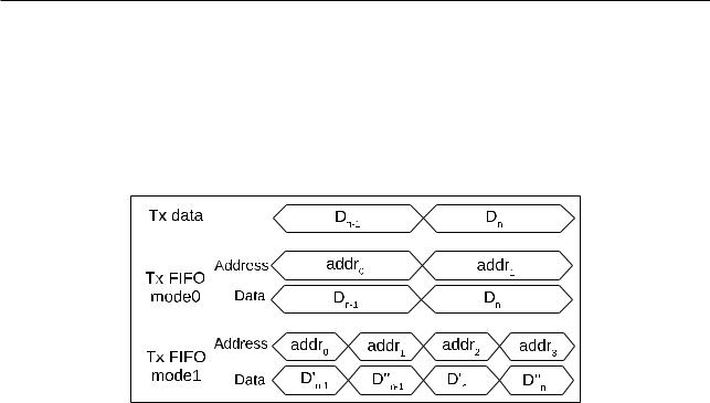
Figure 126. Tx FIFO Data Mode
Table 122. Register Configuration
|
I2S_TX_FIFO_MOD[2:0] |
Description |
|
0 |
16-bit dual channel data |
|
|
|
Tx FIFO mode0 |
2 |
32-bit dual channel data |
|
|
|
|
3 |
32-bit single channel data |
|
|
|
Tx FIFO mode1 |
1 |
16-bit single channel data |
|
|
|
At the first stage, there are two modes for data to be sent and written into FIFO. In Tx FIFO mode0, the Tx data- to-be-sent are written into FIFO according to the time order. In Tx FIFO mode1, the data-to-be-sent are divided into 16 highand 16 low-order bits. Then, both the 16 highand 16 low-order bits are recomposed and written into FIFO. The details are shown in Figure 12-6 with the corresponding registers listed in Table 12-2. Dn′ consists
of 16 high-order bits of Dn and 16 zeros. Dn′′ consists of 16 low-order bits of Dn and 16 zeros. That is to say,
Dn′ = {Dn[31 : 16], 16′h0}, Dn′′ = {Dn[15 : 0], 16′h0}.
At the second stage, the system reads data that will be sent from FIFO, according to the relevant register configuration. The mode in which the system reads data from FIFO is relevant to the configuration of I2S_TX_FIFO_MOD[2.0] and I2S_TX_CHAN_MOD[2:0]. I2S_TX_FIFO_MOD[2.0] determines whether the data are 16-bit or 32-bit, as shown in Table 12-2, while I2S_TX_CHAN_MOD[2:0] determines the format of the data-to-be-sent, as shown in Table 12- 3.
|
|
Table 123. Send Channel Mode |
|
|
|
|
|
|
|
|
|
|
I2S_TX_CHAN_MOD[2:0] |
Description |
|
|
|
|
0 |
Dual channel mode |
|
|
|
|
|
|
|
|
|
|
|
Mono mode |
|
|
|
|
|
When I2S_TX_MSB_RIGHT equals 0, the left-channel data are ”holding” |
|
||
|
1 |
their values and the right-channel data change into the left-channel data. |
|
||
|
|
|
|
|
|
Espressif Systems |
313 |
ESP32 TRM (Version 5.0) |
|||
Submit Documentation Feedback
12 I2S Controller (I2S)
I2S_TX_CHAN_MOD[2:0] |
Description |
|
When I2S_TX_MSB_RIGHT equals 1, the right-channel data are ”holding” |
|
their values and the left-channel data change into the right-channel data. |
|
|
|
Mono mode |
|
When I2S_TX_MSB_RIGHT equals 0, the right-channel data are ”holding” |
2 |
their values and the left-channel data change into the right-channel data. |
|
When I2S_TX_MSB_RIGHT equals 1, the left-channel data are ”holding” |
|
their values and the right-channel data change into the left-channel data. |
|
|
|
Mono mode |
|
When I2S_TX_MSB_RIGHT equals 0, the left-channel data are constants |
3 |
in the range of REG[31:0]. |
|
When I2S_TX_MSB_RIGHT equals 1, the right-channel data are constants |
|
in the range of REG[31:0]. |
|
|
|
Mono mode |
|
When I2S_TX_MSB_RIGHT equals 0, the right-channel data are constants |
4 |
in the range of REG[31:0]. |
|
When I2S_TX_MSB_RIGHT equals 1, the left-channel data are constants |
|
in the range of REG[31:0]. |
|
|
REG[31:0] is the value of register I2S_CONF_SINGLE_DATA_REG[31:0].
The output of the third stage is determined by the mode of the I2S and I2S_TX_BITS_MOD[5:0] bits of register I2S_SAMPLE_RATE_CONF_REG.
12.4.5 Receiving Data
The data-receive phase of the ESP32 I2S module consists of another three stages:
•The input serial-bit stream is transformed into a 64-bit parallel-data stream in I2S mode. In LCD mode, the input parallel-data stream will be extended to a 64-bit parallel-data stream.
•Received data are written into FIFO.
•Data are read from FIFO by CPU/DMA and written into the internal memory.
At the first stage of receiving data, the received-data stream is expanded to a zero-padded parallel-data stream with 32 high-order bits and 32 low-order bits, according to the level of the I2SnI_WS_out (or I2SnI_WS_in) signal. The I2S_RX_MSB_RIGHT bit of register I2S_CONF_REG is used to determine how the data are to be expanded.
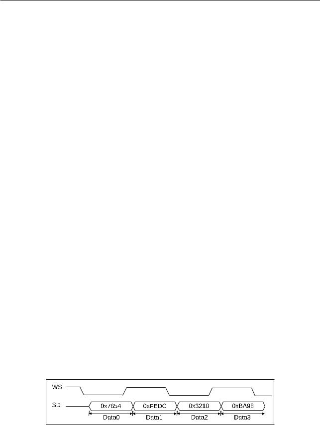
Figure 127. The First Stage of Receiving Data
For example, as is shown in Figure 12-7, if the width of serial data is 16 bits, when I2S_RX_RIGHT_FIRST equals 1, Data0 will be discarded and I2S will start receiving data from Data1. If I2S_RX_MSB_RIGHT equals 1, data of the first stage would be {0xF EDC0000, 0x32100000}. If I2S_RX_MSB_RIGHT equals 0, data of the first
Espressif Systems |
314 |
ESP32 TRM (Version 5.0) |
Submit Documentation Feedback
12 I2S Controller (I2S)
stage would be {0x32100000, 0xF EDC0000}. When I2S_RX_RIGHT_FIRST equals 0, I2S will start receiving data from Data0. If I2S_RX_MSB_RIGHT equals 1, data of the first stage would be {0xF EDC0000, 0x76540000}. If I2S_RX_MSB_RIGHT equals 0, data of the first stage would be {0x76540000, 0xF EDC0000}.
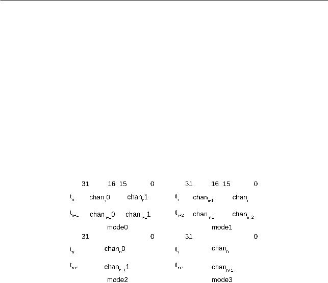
As is shown in Table 12-4 and Figure 12-8, at the second stage, the received data of the Rx unit is written into FIFO. There are four modes of writing received data into FIFO. Each mode corresponds to a value of I2S_RX_FIFO_MOD[2:0] bit.
Table 124. Modes of Writing Received Data into FIFO and the Corresponding Register Configuration
I2S_RX_FIFO_MOD[2:0] |
Data format |
|||||||
0 |
|
|
|
16-bit dual channel data |
||||
|
|
|
|
|
|
|
|
|
1 |
|
|
|
16-bit single channel data |
||||
|
|
|
|
|
|
|
|
|
2 |
|
|
|
32-bit dual channel data |
||||
|
|
|
|
|
|
|
|
|
3 |
|
|
|
32-bit single channel data |
||||
|
|
|
|
|
|
|
|
|
|
|
|
|
|
|
|
|
|
|
|
|
|
|
|
|
|
|
|
|
|
|
|
|
|
|
|
|
|
|
|
|
|
|
|
|
|
|
|
|
|
|
|
|
|
|
|
|
|
|
|
|
|
|
|
|
|
|
|
|
|
|
|
|
|
|
|
|
|
|
|
|
|
|
|
|
|
|
|
|
|
|
|
|
|
|
|
|
|
|
Figure 128. Modes of Writing Received Data into FIFO
At the third stage, CPU or DMA will read data from FIFO and write them into the internal memory directly. The register configuration that each mode corresponds to is shown in Table 12-5.
Table 125. The Register Configuration to Which the Four Modes Correspond
I2S_RX_MSB_RIGHT |
I2S_RX_CHAN_MOD |
mode0 |
mode1 |
|
mode2 |
mode3 |
|
|
|
0 |
|
- |
|
|
- |
|
|
|
|
|
|
|
|
|
|
|
|
1 |
|
left channel |
+ |
|
left channel |
+ |
|
|
left channel |
left channel |
|
left channel |
left channel |
|
||
0 |
|
|
|
|||||
|
|
|
|
|
|
|
||
2 |
+ right channel |
right channel + |
+ right channel |
right channel + |
||||
|
||||||||
|
|
right channel |
|
|
right channel |
|
||
|
|
|
|
|
|
|||
|
|
|
|
|
|
|
|
|
|
3 |
|
- |
|
|
- |
|
|
|
|
|
|
|
|
|
|
|
|
0 |
|
- |
|
|
- |
|
|
|
|
|
|
|
|
|||
|
1 |
|
right channel + |
|
right channel + |
|||
|
right channel |
right channel |
|
right channel |
right channel |
|
||
1 |
|
|
|
|||||
|
|
|
|
|
|
|
||
2 |
+ left channel |
left channel |
+ |
+ left channel |
left channel |
+ |
||
|
||||||||
|
|
left channel |
|
|
left channel |
|
||
|
|
|
|
|
|
|||
|
|
|
|
|
|
|
|
|
|
3 |
|
- |
|
|
- |
|
|
|
|
|
|
|
|
|
|
|
Espressif Systems |
315 |
|
|
ESP32 TRM (Version 5.0) |
|
|||
Submit Documentation Feedback
12 I2S Controller (I2S)
12.4.6 I2S Master/Slave Mode
The ESP32 I2S module can be configured to act as a master or slave device on the I2S bus. The module supports slave transmitter and receiver configurations in addition to master transmitter and receiver configurations. All these modes can support full-duplex and half-duplex communication over the I2S bus.
I2S_RX_SLAVE_MOD bit and I2S_TX_SLAVE_MOD bit of register I2S_CONF_REG can configure I2S to slave receiving mode and slave transmitting mode, respectively.
I2S_TX_START bit of register I2S_CONF_REG is used to enable transmission. When I2S is in master transmitting mode and this bit is set, the module will keep driving the clock signal and data of left and right channels. If FIFO sends out all the buffered data and there are no new data to shift, the last batch of data will be looped on the data line. When this bit is reset, master will stop driving clock and data lines. When I2S is configured to slave transmitting mode and this bit is set, the module will wait for the master BCK clock to enable a transmit operation.
The I2S_RX_START bit of register I2S_CONF_REG is used to enable a receive operation. When I2S is in master receiving mode and this bit is set, the module will keep driving the clock signal and sampling the input data stream until this bit is reset. If I2S is configured to slave receiving mode and this bit is set, the receiving module will wait for the master BCK clock to enable a receiving operation.
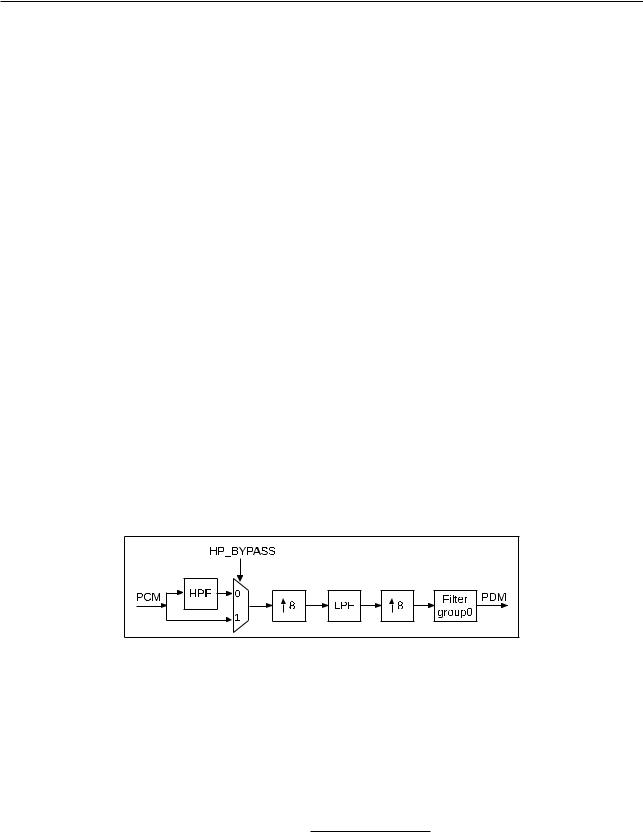
12.4.7 I2S PDM
As is shown in Figure 12-1, ESP32 I2S0 allows for pulse density modulation (PDM), which enables fast conversion between pulse code modulation (PCM) and PDM signals.
The output clock of PDM is mapped to the I2S0*_WS_out signal. Its configuration is identical to I2S’s BCK. Please refer to section 12.3, ”The Clock of I2S Module”, for further details. The bit width for both received and transmitted I2S PCM signals is 16 bits.
Figure 129. PDM Transmitting Module
The PDM transmitting module is used to convert PCM signals into PDM signals, as shown in Figure 12-9. HPF is a high-speed channel filter, and LPF is a low-speed channel filter. The PDM signal is derived from the PCM signal, after upsampling and filtering. Signal I2S_TX_PDM_HP_BYPASS of register I2S_PDM_CONF_REG can be set to bypass the HPF at the PCM input. Filter module group0 carries out the upsampling. If the frequency of the PDM signal is fpdm and the frequency of the PCM signal is fpcm, the relation between fpdm and fpcm is given by:
I2S_T X_P DM_F P
fpdm = 64×fpcm× I2S_T X_P DM_F S
The upsampling factor of 64 is the result of the two upsampling stages.
Table 12-6 lists the configuration rates of the I2S_TX_PDM_FP bit and the I2S_TX_PDM_FS bit of register I2S_PDM _FREQ_CONF_REG, whose output PDM signal frequency remains 48×128 KHz at different PCM signal frequencies.
Espressif Systems |
316 |
ESP32 TRM (Version 5.0) |
Submit Documentation Feedback
12 I2S Controller (I2S)
Table 126. Upsampling Rate Configuration
fpcm (KHz) |
I2S_TX_PDM_FP |
I2S_TX_PDM_FS |
fpdm (KHz) |
|
48 |
960 |
480 |
|
|
|
|
|
|
|
44.1 |
960 |
441 |
|
|
|
|
|
|
|
32 |
960 |
320 |
48×128 |
|
|
|
|
||
24 |
960 |
240 |
||
|
||||
|
|
|
|
|
16 |
960 |
160 |
|
|
|
|
|
|
|
8 |
960 |
80 |
|
|
|
|
|
|
The I2S_TX_PDM_SINC_OSR2 bit of I2S_PDM_CONF_REG is the upsampling rate of the Filter group0.
I2S_T X_P DM_SINC_OSR2 = |
I2S_T X_P DM_F P |
|
I2S_T X_P DM_F S |
As is shown in Figure 12-10, the I2S_TX_PDM_EN bit and the I2S_PCM2PDM_CONV_EN bit of register I2S_PDM_ CONF_REG should be set to 1 to use the PDM sending module. The I2S_TX_PDM_SIGMADELTA_IN_SHIFT bit, I2S_TX_PDM_SINC_IN_SHIFT bit, I2S_TX_PDM_LP_IN_SHIFT bit and I2S_TX_PDM_HP_IN_SHIFT bit of register I2S_PDM_CONF_REG are used to adjust the size of the input signal of each filter module.
Figure 1210. PDM Sends Signal
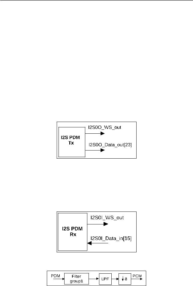
As is shown in Figure 12-11, the I2S_RX_PDM_EN bit and the I2S_PDM2PCM_CONV_EN bit of register I2S_PDM_ CONF_REG should be set to 1, in order to use the PDM receiving module. As is shown in Figure 12-12, the PDM receiving module will convert the received PDM signal into a 16-bit PCM signal. Filter group1 is used to downsample the PDM signal, and the I2S_RX_PDM_SINC_DSR_16_EN bit of register I2S_PDM_CONF_REG is used to adjust the corresponding down-sampling rate.
Figure 1211. PDM Receives Signal
Figure 1212. PDM Receive Module
Espressif Systems |
317 |
ESP32 TRM (Version 5.0) |
Submit Documentation Feedback