

- •1 System and Memory
- •1.1 Introduction
- •1.2 Features
- •1.3 Functional Description
- •1.3.1 Address Mapping
- •1.3.2 Embedded Memory
- •1.3.3 External Memory
- •1.3.5 Peripherals
- •2 Interrupt Matrix (INTERRUPT)
- •2.1 Overview
- •2.2 Features
- •2.3 Functional Description
- •2.3.1 Peripheral Interrupt Source
- •2.3.2 CPU Interrupt
- •2.3.3 Allocate Peripheral Interrupt Sources to Peripheral Interrupt on CPU
- •2.3.4 CPU NMI Interrupt Mask
- •2.3.5 Query Current Interrupt Status of Peripheral Interrupt Source
- •2.4 Registers
- •3 Reset and Clock
- •3.1 System Reset
- •3.1.1 Introduction
- •3.1.2 Reset Source
- •3.2 System Clock
- •3.2.1 Introduction
- •3.2.3 CPU Clock
- •3.2.4 Peripheral Clock
- •3.2.7 Audio PLL
- •3.3 Register Summary
- •3.4 Registers
- •4.1 Overview
- •4.2 Peripheral Input via GPIO Matrix
- •4.2.1 Summary
- •4.2.2 Functional Description
- •4.2.3 Simple GPIO Input
- •4.3 Peripheral Output via GPIO Matrix
- •4.3.1 Summary
- •4.3.3 Simple GPIO Output
- •4.4 Direct I/O via IO_MUX
- •4.4.1 Summary
- •4.4.2 Functional Description
- •4.5 RTC IO_MUX for Low Power and Analog I/O
- •4.5.1 Summary
- •4.5.2 Analog Function Description
- •4.7 Pad Hold Feature
- •4.8 I/O Pad Power Supplies
- •4.8.1 VDD_SDIO Power Domain
- •4.9 Peripheral Signal List
- •4.10 IO_MUX Pad List
- •4.11 RTC_MUX Pin List
- •4.12 Register Summary
- •4.12.1 GPIO Matrix Register Summary
- •4.12.2 IO MUX Register Summary
- •4.12.3 RTC IO MUX Register Summary
- •4.13 Registers
- •4.13.1 GPIO Matrix Registers
- •4.13.2 IO MUX Registers
- •4.13.3 RTC IO MUX Registers
- •5 DPort Registers
- •5.1 Introduction
- •5.2 Features
- •5.3 Functional Description
- •5.3.1 System and Memory Register
- •5.3.2 Reset and Clock Registers
- •5.3.3 Interrupt Matrix Register
- •5.3.4 DMA Registers
- •5.3.5 MPU/MMU Registers
- •5.3.7 Peripheral Clock Gating and Reset
- •5.4 Register Summary
- •5.5 Registers
- •6 DMA Controller (DMA)
- •6.1 Overview
- •6.2 Features
- •6.3 Functional Description
- •6.3.1 DMA Engine Architecture
- •6.3.2 Linked List
- •6.4 UART DMA (UDMA)
- •7 SPI Controller (SPI)
- •7.1 Overview
- •7.5 Parallel QSPI
- •7.5.1 Communication Format of Parallel QSPI
- •7.6.1 SPI Interrupts
- •7.6.2 DMA Interrupts
- •7.7 Register Summary
- •7.8 Registers
- •8 SDIO Slave Controller
- •8.1 Overview
- •8.2 Features
- •8.3 Functional Description
- •8.3.1 SDIO Slave Block Diagram
- •8.3.3 Register Access
- •8.3.6 SDIO Bus Timing
- •8.3.7 Interrupt
- •8.4 Register Summary
- •8.5 SLC Registers
- •8.6 SLC Host Registers
- •8.7 HINF Registers
- •9 SD/MMC Host Controller
- •9.1 Overview
- •9.2 Features
- •9.3 SD/MMC External Interface Signals
- •9.4 Functional Description
- •9.4.1 SD/MMC Host Controller Architecture
- •9.4.2 Command Path
- •9.4.3 Data Path
- •9.5 Software Restrictions for Proper CIU Operation
- •9.6 RAM for Receiving and Sending Data
- •9.6.1 Transmit RAM Module
- •9.6.2 Receive RAM Module
- •9.8 The Structure of a Linked List
- •9.9 Initialization
- •9.9.1 DMAC Initialization
- •9.9.2 DMAC Transmission Initialization
- •9.9.3 DMAC Reception Initialization
- •9.11 Interrupt
- •9.12 Register Summary
- •9.13 Registers
- •10 Ethernet Media Access Controller (MAC)
- •10.1 Overview
- •10.2 EMAC_CORE
- •10.2.1 Transmit Operation
- •10.2.2 Receive Operation
- •10.3 MAC Interrupt Controller
- •10.4 MAC Address Filtering
- •10.4.1 Unicast Destination Address Filtering
- •10.4.2 Multicast Destination Address Filtering
- •10.4.3 Broadcast Address Filtering
- •10.4.4 Unicast Source Address Filtering
- •10.4.5 Inverse Filtering Operation
- •10.4.6 Good Transmitted Frames and Received Frames
- •10.5 EMAC_MTL (MAC Transaction Layer)
- •10.6 PHY Interface
- •10.6.1 MII (Media Independent Interface)
- •10.6.3 Station Management Agent (SMA) Interface
- •10.6.4 RMII Timing
- •10.7 Ethernet DMA Features
- •10.8 Linked List Descriptors
- •10.8.1 Transmit Descriptors
- •10.8.2 Receive Descriptors
- •10.9 Register Summary
- •10.10 Registers
- •11 I2C Controller (I2C)
- •11.1 Overview
- •11.2 Features
- •11.3 Functional Description
- •11.3.1 Introduction
- •11.3.2 Architecture
- •11.3.3 I2C Bus Timing
- •11.3.7 Interrupts
- •11.4 Register Summary
- •11.5 Registers
- •12 I2S Controller (I2S)
- •12.1 Overview
- •12.2 Features
- •12.3 The Clock of I2S Module
- •12.4 I2S Mode
- •12.4.1 Supported Audio Standards
- •12.4.2 Module Reset
- •12.4.3 FIFO Operation
- •12.4.5 Receiving Data
- •12.5.1 LCD Master Transmitting Mode
- •12.5.2 Camera Slave Receiving Mode
- •12.5.3 ADC/DAC mode
- •12.6 I2S Interrupts
- •12.6.1 FIFO Interrupts
- •12.6.2 DMA Interrupts
- •12.7 Register Summary
- •12.8 Registers
- •13 UART Controller (UART)
- •13.1 Overview
- •13.2 UART Features
- •13.3 Functional Description
- •13.3.1 Introduction
- •13.3.3 UART RAM
- •13.3.5 UART Data Frame
- •13.3.7 Flow Control
- •13.3.8 UART DMA
- •13.3.9 UART Interrupts
- •13.3.10 UHCI Interrupts
- •13.4 Register Summary
- •13.4.1 UART Register Summary
- •13.5 Registers
- •13.5.1 UART Registers
- •13.5.2 UHCI Registers
- •14 LED PWM Controller (LEDC)
- •14.1 Introduction
- •14.2 Functional Description
- •14.2.1 Architecture
- •14.2.3 Channels
- •14.2.4 Interrupts
- •14.3 Register Summary
- •14.4 Registers
- •15 Remote Control Peripheral (RMT)
- •15.1 Introduction
- •15.2 Functional Description
- •15.2.1 RMT Architecture
- •15.2.3 Clock
- •15.2.4 Transmitter
- •15.2.5 Receiver
- •15.2.6 Interrupts
- •15.3 Register Summary
- •15.4 Registers
- •16 Motor Control PWM (PWM)
- •16.1 Introduction
- •16.2 Features
- •16.3 Submodules
- •16.3.1 Overview
- •16.3.2 PWM Timer Submodule
- •16.3.3 PWM Operator Submodule
- •16.3.4 Capture Submodule
- •16.4 Register Summary
- •16.5 Registers
- •17 Pulse Count Controller (PCNT)
- •17.1 Overview
- •17.2 Functional Description
- •17.2.1 Architecture
- •17.2.2 Counter Channel Inputs
- •17.2.3 Watchpoints
- •17.2.4 Examples
- •17.2.5 Interrupts
- •18 Timer Group (TIMG)
- •18.1 Introduction
- •18.2 Functional Description
- •18.2.2 64-bit Time-base Counter
- •18.2.3 Alarm Generation
- •18.2.4 MWDT
- •18.2.5 Interrupts
- •18.3 Register Summary
- •18.4 Registers
- •19 Watchdog Timers (WDT)
- •19.1 Introduction
- •19.2 Features
- •19.3 Functional Description
- •19.3.1 Clock
- •20 eFuse Controller
- •20.1 Introduction
- •20.2 Features
- •20.3 Functional Description
- •20.3.1 Structure
- •20.3.3 Software Reading of System Parameters
- •20.3.4 The Use of System Parameters by Hardware Modules
- •20.3.5 Interrupts
- •20.4 Register Summary
- •20.5 Registers
- •21 Two-wire Automotive Interface (TWAI)
- •21.1 Overview
- •21.2 Features
- •21.3 Functional Protocol
- •21.3.1 TWAI Properties
- •21.3.2 TWAI Messages
- •21.3.3 TWAI Errors
- •21.3.4 TWAI Bit Timing
- •21.4 Architectural Overview
- •21.4.1 Registers Block
- •21.4.2 Bit Stream Processor
- •21.4.3 Error Management Logic
- •21.4.4 Bit Timing Logic
- •21.4.5 Acceptance Filter
- •21.5 Functional Description
- •21.5.1 Modes
- •21.5.2 Bit Timing
- •21.5.3 Interrupt Management
- •21.5.4 Transmit and Receive Buffers
- •21.5.5 Receive FIFO and Data Overruns
- •21.5.6 Acceptance Filter
- •21.5.8 Error Code Capture
- •21.5.9 Arbitration Lost Capture
- •21.6 Register Summary
- •21.7 Registers
- •22 AES Accelerator (AES)
- •22.1 Introduction
- •22.2 Features
- •22.3 Functional Description
- •22.3.1 AES Algorithm Operations
- •22.3.2 Key, Plaintext and Ciphertext
- •22.3.3 Endianness
- •22.3.4 Encryption and Decryption Operations
- •22.3.5 Speed
- •22.4 Register Summary
- •22.5 Registers
- •23 SHA Accelerator (SHA)
- •23.1 Introduction
- •23.2 Features
- •23.3 Functional Description
- •23.3.1 Padding and Parsing the Message
- •23.3.2 Message Digest
- •23.3.3 Hash Operation
- •23.3.4 Speed
- •23.4 Register Summary
- •23.5 Registers
- •24 RSA Accelerator (RSA)
- •24.1 Introduction
- •24.2 Features
- •24.3 Functional Description
- •24.3.1 Initialization
- •24.3.2 Large Number Modular Exponentiation
- •24.3.4 Large Number Multiplication
- •24.4 Register Summary
- •24.5 Registers
- •25 Random Number Generator (RNG)
- •25.1 Introduction
- •25.2 Feature
- •25.3 Functional Description
- •25.5 Register Summary
- •25.6 Register
- •26 External Memory Encryption and Decryption (FLASH)
- •26.1 Overview
- •26.2 Features
- •26.3 Functional Description
- •26.3.1 Key Generator
- •26.3.2 Flash Encryption Block
- •26.3.3 Flash Decryption Block
- •26.4 Register Summary
- •26.5 Register
- •27 Memory Management and Protection Units (MMU, MPU)
- •27.1 Introduction
- •27.2 Features
- •27.3 Functional Description
- •27.3.1 PID Controller
- •28 Process ID Controller (PID)
- •28.1 Overview
- •28.2 Features
- •28.3 Functional Description
- •28.3.1 Interrupt Identification
- •28.3.2 Information Recording
- •28.3.3 Proactive Process Switching
- •28.4 Register Summary
- •28.5 Registers
- •29 On-Chip Sensors and Analog Signal Processing
- •29.1 Introduction
- •29.2 Capacitive Touch Sensor
- •29.2.1 Introduction
- •29.2.2 Features
- •29.2.3 Available GPIOs
- •29.2.4 Functional Description
- •29.2.5 Touch FSM
- •29.3.1 Introduction
- •29.3.2 Features
- •29.3.3 Outline of Function
- •29.3.4 RTC SAR ADC Controllers
- •29.3.5 DIG SAR ADC Controllers
- •29.4.1 Introduction
- •29.4.2 Features
- •29.4.4 Cosine Waveform Generator
- •29.5 Register Summary
- •29.5.1 Sensors
- •29.5.2 Advanced Peripheral Bus
- •29.6 Registers
- •29.6.1 Sensors
- •29.6.2 Advanced Peripheral Bus
- •30 ULP Coprocessor (ULP)
- •30.1 Introduction
- •30.2 Features
- •30.4 Instruction Set
- •30.4.2 ST – Store Data in Memory
- •30.4.3 LD – Load Data from Memory
- •30.4.4 JUMP – Jump to an Absolute Address
- •30.4.5 JUMPR – Jump to a Relative Offset (Conditional upon R0)
- •30.4.7 HALT – End the Program
- •30.4.8 WAKE – Wake up the Chip
- •30.4.10 WAIT – Wait for a Number of Cycles
- •30.4.12 I2C_RD/I2C_WR – Read/Write I²C
- •30.4.13 REG_RD – Read from Peripheral Register
- •30.5 ULP Program Execution
- •30.6 RTC_I2C Controller
- •30.6.1 Configuring RTC_I2C
- •30.6.2 Using RTC_I2C
- •30.7 Register Summary
- •30.7.1 SENS_ULP Address Space
- •30.7.2 RTC_I2C Address Space
- •30.8 Registers
- •30.8.1 SENS_ULP Address Space
- •30.8.2 RTC_I2C Address Space
- •31 Low-Power Management (RTC_CNTL)
- •31.1 Introduction
- •31.2 Features
- •31.3 Functional Description
- •31.3.2 Digital Core Voltage Regulator
- •31.3.4 Flash Voltage Regulator
- •31.3.5 Brownout Detector
- •31.3.6 RTC Module
- •31.3.9 Predefined Power Modes
- •31.3.10 Wakeup Source
- •31.3.12 RTC Timer
- •31.3.13 RTC Boot
- •31.4 Register Summary
- •31.5 Registers
- •Glossary
- •Abbreviations for Peripherals
- •Abbreviations for Registers
- •Revision History
12 I2S Controller (I2S)
12 I2S Controller (I2S)
12.1Overview
The I2S bus provides a flexible communication interface for streaming digital data in multimedia applications, especially digital audio applications. The ESP32 includes two I2S interfaces: I2S0 and I2S1.
The I2S standard bus defines three signals: a clock signal, a channel selection signal, and a serial data signal. A basic I2S data bus has one master and one slave. The roles remain unchanged throughout the communication. The I2S modules on the ESP32 provide separate transmit and receive channels for high performance.
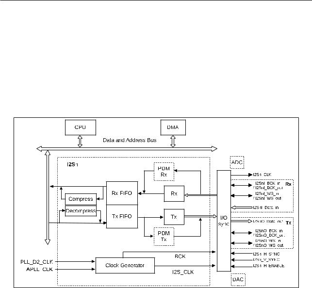
Figure 121. I2S System Block Diagram
Figure 12-1 is the system block diagram of the ESP32 I2S module. In the figure above, the value of ”n” can be either 0 or 1. There are two independent I2S modules embedded in ESP32, namely I2S0 and I2S1. Each I2S module contains a Tx (transmit) unit and a Rx (receive) unit. Both the Tx unit and the Rx unit have a three-wire interface that includes a clock line, a channel selection line and a serial data line. The serial data line of the Tx unit is fixed as output, and the serial data line of the Rx unit is fixed as input. The clock line and the channel selection line of the Tx and Rx units can be configured to both master transmitting mode and slave receiving mode. In the LCD mode, the serial data line extends to the parallel data bus. Both the Tx unit and the Rx unit have a 32-bit-wide FIFO with a depth of 64. Besides, only I2S0 supports on-chip DAC/ADC modes, as well as receiving and transmitting PDM signals.
The right side of Figure 12-1 shows the signal bus of the I2S module. The signal naming rule of the Rx and Tx units is I2SnA_B_C, where ”n” stands for either I2S0 or I2S1; ”A” represents the direction of I2S module’s data bus signal, ”I” represents input, ”O” represents output; ”B” represents signal function; ”C” represents the signal direction, ”in” means that the signal is input into the I2S module, while ”out” means that the I2S module outputs the signal. For a detailed description of the I2S signal bus, please refer to Table 12-1. Table 12-1 describes the signal bus of the I2S module. Except for the I2Sn_CLK signal, all other signals are mapped to the chip pin via the
Espressif Systems |
308 |
ESP32 TRM (Version 5.0) |
Submit Documentation Feedback

12 I2S Controller (I2S)
GPIO matrix and IO MUX. The I2Sn_CLK signal is mapped to the chip pin via the IO_MUX. For details, please refer to the chapter about IO_MUX and the GPIO Matrix.
Table 121. I2S Signal Bus Description
Signal Bus |
Signal Direction |
Data Signal Direction |
|
I2SnI_BCK_in |
In slave mode, I2S module inputs signals. |
I2S module receives data. |
|
|
|
|
|
I2SnI_BCK_out |
In master mode, I2S module outputs signals. |
I2S module receives data. |
|
|
|
|
|
I2SnI_WS_in |
In slave mode, I2S module inputs signals. |
I2S module receives data. |
|
|
|
|
|
I2SnI_WS_out |
In master mode, I2S module outputs signals. |
I2S module receives data. |
|
|
|
|
|
|
|
In I2S mode, I2SnI_Data_in[15] is the |
|
I2SnI_Data_in1 |
I2S module inputs signals. |
serial data bus of I2S. In LCD mode, |
|
the data bus width can be configured |
|||
|
|
||
|
|
as needed. |
|
|
|
|
|
|
|
In I2S mode, I2SnO_Data_out[23] is |
|
I2SnO_Data_out1 |
I2S module outputs signals. |
the serial data bus of I2S. In LCD |
|
mode, the data bus width can be |
|||
|
|
||
|
|
configured as needed. |
|
|
|
|
|
I2SnO_BCK_in |
In slave mode, I2S module inputs signals. |
I2S module sends data. |
|
|
|
|
|
I2SnO_BCK_out |
In master mode, I2S module outputs signals. |
I2S module sends data. |
|
|
|
|
|
I2SnO_WS_in |
In slave mode, I2S module inputs signals. |
I2S module sends data. |
|
|
|
|
|
I2SnO_WS_out |
In master mode, I2S module outputs signals. |
I2S module sends data. |
|
|
|
|
|
I2Sn_CLK2 |
I2S module outputs signals. |
It is used as a clock source for pe- |
|
ripheral chips. |
|||
|
|
||
|
|
|
|
I2Sn_H_SYNC |
|
|
|
|
|
|
|
I2Sn_V_SYNC |
In Camera mode, I2S module inputs signals. |
The signals are sent from the Camera. |
|
|
|
|
|
I2Sn_H_ENABLE |
|
|
|
|
|
|
Note:
1.Assume that the bit width of the input/output signal is N, the input signal should be configured to I2SnI_Data_in[N- 1:0], and the output signal to I2SnO_Data_out[23:23-N+1]. Generally, for input signals, N=8 or 16; while for output signals, N=8, 16 or 24 (note that I2S1 does not support 24-bit width).
2.I2Sn_CLK can only be mapped to GPIO0, U0RXD (GPIO3) or U0TXD (GPIO1) by selecting GPIO functions CLK_OUT1, CLK_OUT2, or CLK_OUT3. For more information, see Table 4-3: IO_MUX Pad List.
12.2Features
I2S mode
•Configurable high-precision output clock
•Full-duplex and half-duplex data transmit and receive modes
•Supports multiple digital audio standards
•Embedded A-law compression/decompression module
•Configurable clock signal
Espressif Systems |
309 |
ESP32 TRM (Version 5.0) |
Submit Documentation Feedback
12I2S Controller (I2S)
•Supports PDM signal input and output
•Configurable data transmit and receive modes LCD mode
•Supports multiple LCD modes, including external LCD
•Supports external Camera
•Supports on-chip DAC/ADC modes
I2S interrupts
•Standard I2S interface interrupts
•I2S DMA interface interrupts
12.3The Clock of I2S Module
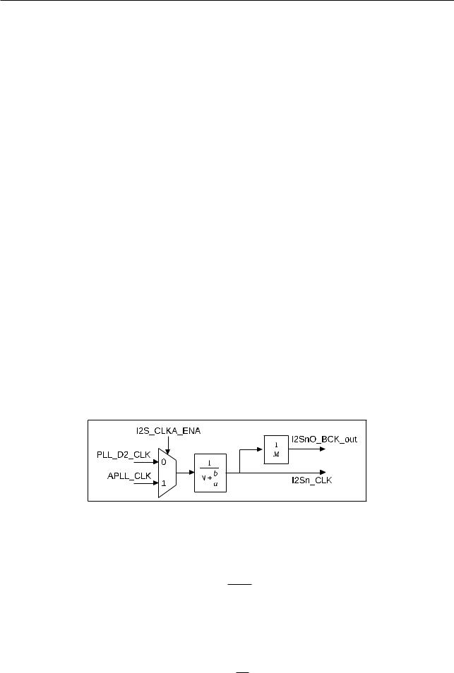
As is shown in Figure 12-2, I2Sn_CLK, as the master clock of I2S module, is derived from the 160 MHz clock PLL_F160M_CLK or the configurable analog PLL output clock APLL_CLK. The serial clock (BCK) of the I2S module is derived from I2Sn_CLK. The I2S_CLKA_ENA bit of register I2S_CLKM_CONF_REG is used to select either PLL_F160M_CLK or APLL_CLK as the clock source for I2Sn. PLL_F160_CLK is used as the clock source for I2Sn, by default.
Notice:
•When using PLL_F160M_CLK as the clock source, it is not recommended to divide it using decimals. For high performance audio applications, the analog PLL output clock source APLL_CLK must be used to acquire highly accurate I2Sn_CLK and BCK. For further details, please refer to the chapter entitled Reset and Clock.
•When ESP32 I2S works in slave mode, the master must use I2Sn_CLK as the master clock and fi2s >= 8 *
fBCK.
Figure 122. I2S Clock
The relation between I2Sn_CLK frequency fi2s and the divider clock source frequency fpll can be seen in the equation below:
fpll fi2s = N + ba
”N”, whose value is >=2, corresponds to the REG _CLKM_DIV_NUM [7:0] bits of register I2S_CLKM_CONF_REG , ”b” is the I2S_CLKM_DIV_B[5:0] bit and ”a” is the I2S_CLKM_DIV_A[5:0] bit.
In master mode, the serial clock BCK in the I2S module is derived from I2Sn_CLK, that is:
fi2s fBCK = M
Espressif Systems |
310 |
ESP32 TRM (Version 5.0) |
Submit Documentation Feedback