

- •1 System and Memory
- •1.1 Introduction
- •1.2 Features
- •1.3 Functional Description
- •1.3.1 Address Mapping
- •1.3.2 Embedded Memory
- •1.3.3 External Memory
- •1.3.5 Peripherals
- •2 Interrupt Matrix (INTERRUPT)
- •2.1 Overview
- •2.2 Features
- •2.3 Functional Description
- •2.3.1 Peripheral Interrupt Source
- •2.3.2 CPU Interrupt
- •2.3.3 Allocate Peripheral Interrupt Sources to Peripheral Interrupt on CPU
- •2.3.4 CPU NMI Interrupt Mask
- •2.3.5 Query Current Interrupt Status of Peripheral Interrupt Source
- •2.4 Registers
- •3 Reset and Clock
- •3.1 System Reset
- •3.1.1 Introduction
- •3.1.2 Reset Source
- •3.2 System Clock
- •3.2.1 Introduction
- •3.2.3 CPU Clock
- •3.2.4 Peripheral Clock
- •3.2.7 Audio PLL
- •3.3 Register Summary
- •3.4 Registers
- •4.1 Overview
- •4.2 Peripheral Input via GPIO Matrix
- •4.2.1 Summary
- •4.2.2 Functional Description
- •4.2.3 Simple GPIO Input
- •4.3 Peripheral Output via GPIO Matrix
- •4.3.1 Summary
- •4.3.3 Simple GPIO Output
- •4.4 Direct I/O via IO_MUX
- •4.4.1 Summary
- •4.4.2 Functional Description
- •4.5 RTC IO_MUX for Low Power and Analog I/O
- •4.5.1 Summary
- •4.5.2 Analog Function Description
- •4.7 Pad Hold Feature
- •4.8 I/O Pad Power Supplies
- •4.8.1 VDD_SDIO Power Domain
- •4.9 Peripheral Signal List
- •4.10 IO_MUX Pad List
- •4.11 RTC_MUX Pin List
- •4.12 Register Summary
- •4.12.1 GPIO Matrix Register Summary
- •4.12.2 IO MUX Register Summary
- •4.12.3 RTC IO MUX Register Summary
- •4.13 Registers
- •4.13.1 GPIO Matrix Registers
- •4.13.2 IO MUX Registers
- •4.13.3 RTC IO MUX Registers
- •5 DPort Registers
- •5.1 Introduction
- •5.2 Features
- •5.3 Functional Description
- •5.3.1 System and Memory Register
- •5.3.2 Reset and Clock Registers
- •5.3.3 Interrupt Matrix Register
- •5.3.4 DMA Registers
- •5.3.5 MPU/MMU Registers
- •5.3.7 Peripheral Clock Gating and Reset
- •5.4 Register Summary
- •5.5 Registers
- •6 DMA Controller (DMA)
- •6.1 Overview
- •6.2 Features
- •6.3 Functional Description
- •6.3.1 DMA Engine Architecture
- •6.3.2 Linked List
- •6.4 UART DMA (UDMA)
- •7 SPI Controller (SPI)
- •7.1 Overview
- •7.5 Parallel QSPI
- •7.5.1 Communication Format of Parallel QSPI
- •7.6.1 SPI Interrupts
- •7.6.2 DMA Interrupts
- •7.7 Register Summary
- •7.8 Registers
- •8 SDIO Slave Controller
- •8.1 Overview
- •8.2 Features
- •8.3 Functional Description
- •8.3.1 SDIO Slave Block Diagram
- •8.3.3 Register Access
- •8.3.6 SDIO Bus Timing
- •8.3.7 Interrupt
- •8.4 Register Summary
- •8.5 SLC Registers
- •8.6 SLC Host Registers
- •8.7 HINF Registers
- •9 SD/MMC Host Controller
- •9.1 Overview
- •9.2 Features
- •9.3 SD/MMC External Interface Signals
- •9.4 Functional Description
- •9.4.1 SD/MMC Host Controller Architecture
- •9.4.2 Command Path
- •9.4.3 Data Path
- •9.5 Software Restrictions for Proper CIU Operation
- •9.6 RAM for Receiving and Sending Data
- •9.6.1 Transmit RAM Module
- •9.6.2 Receive RAM Module
- •9.8 The Structure of a Linked List
- •9.9 Initialization
- •9.9.1 DMAC Initialization
- •9.9.2 DMAC Transmission Initialization
- •9.9.3 DMAC Reception Initialization
- •9.11 Interrupt
- •9.12 Register Summary
- •9.13 Registers
- •10 Ethernet Media Access Controller (MAC)
- •10.1 Overview
- •10.2 EMAC_CORE
- •10.2.1 Transmit Operation
- •10.2.2 Receive Operation
- •10.3 MAC Interrupt Controller
- •10.4 MAC Address Filtering
- •10.4.1 Unicast Destination Address Filtering
- •10.4.2 Multicast Destination Address Filtering
- •10.4.3 Broadcast Address Filtering
- •10.4.4 Unicast Source Address Filtering
- •10.4.5 Inverse Filtering Operation
- •10.4.6 Good Transmitted Frames and Received Frames
- •10.5 EMAC_MTL (MAC Transaction Layer)
- •10.6 PHY Interface
- •10.6.1 MII (Media Independent Interface)
- •10.6.3 Station Management Agent (SMA) Interface
- •10.6.4 RMII Timing
- •10.7 Ethernet DMA Features
- •10.8 Linked List Descriptors
- •10.8.1 Transmit Descriptors
- •10.8.2 Receive Descriptors
- •10.9 Register Summary
- •10.10 Registers
- •11 I2C Controller (I2C)
- •11.1 Overview
- •11.2 Features
- •11.3 Functional Description
- •11.3.1 Introduction
- •11.3.2 Architecture
- •11.3.3 I2C Bus Timing
- •11.3.7 Interrupts
- •11.4 Register Summary
- •11.5 Registers
- •12 I2S Controller (I2S)
- •12.1 Overview
- •12.2 Features
- •12.3 The Clock of I2S Module
- •12.4 I2S Mode
- •12.4.1 Supported Audio Standards
- •12.4.2 Module Reset
- •12.4.3 FIFO Operation
- •12.4.5 Receiving Data
- •12.5.1 LCD Master Transmitting Mode
- •12.5.2 Camera Slave Receiving Mode
- •12.5.3 ADC/DAC mode
- •12.6 I2S Interrupts
- •12.6.1 FIFO Interrupts
- •12.6.2 DMA Interrupts
- •12.7 Register Summary
- •12.8 Registers
- •13 UART Controller (UART)
- •13.1 Overview
- •13.2 UART Features
- •13.3 Functional Description
- •13.3.1 Introduction
- •13.3.3 UART RAM
- •13.3.5 UART Data Frame
- •13.3.7 Flow Control
- •13.3.8 UART DMA
- •13.3.9 UART Interrupts
- •13.3.10 UHCI Interrupts
- •13.4 Register Summary
- •13.4.1 UART Register Summary
- •13.5 Registers
- •13.5.1 UART Registers
- •13.5.2 UHCI Registers
- •14 LED PWM Controller (LEDC)
- •14.1 Introduction
- •14.2 Functional Description
- •14.2.1 Architecture
- •14.2.3 Channels
- •14.2.4 Interrupts
- •14.3 Register Summary
- •14.4 Registers
- •15 Remote Control Peripheral (RMT)
- •15.1 Introduction
- •15.2 Functional Description
- •15.2.1 RMT Architecture
- •15.2.3 Clock
- •15.2.4 Transmitter
- •15.2.5 Receiver
- •15.2.6 Interrupts
- •15.3 Register Summary
- •15.4 Registers
- •16 Motor Control PWM (PWM)
- •16.1 Introduction
- •16.2 Features
- •16.3 Submodules
- •16.3.1 Overview
- •16.3.2 PWM Timer Submodule
- •16.3.3 PWM Operator Submodule
- •16.3.4 Capture Submodule
- •16.4 Register Summary
- •16.5 Registers
- •17 Pulse Count Controller (PCNT)
- •17.1 Overview
- •17.2 Functional Description
- •17.2.1 Architecture
- •17.2.2 Counter Channel Inputs
- •17.2.3 Watchpoints
- •17.2.4 Examples
- •17.2.5 Interrupts
- •18 Timer Group (TIMG)
- •18.1 Introduction
- •18.2 Functional Description
- •18.2.2 64-bit Time-base Counter
- •18.2.3 Alarm Generation
- •18.2.4 MWDT
- •18.2.5 Interrupts
- •18.3 Register Summary
- •18.4 Registers
- •19 Watchdog Timers (WDT)
- •19.1 Introduction
- •19.2 Features
- •19.3 Functional Description
- •19.3.1 Clock
- •20 eFuse Controller
- •20.1 Introduction
- •20.2 Features
- •20.3 Functional Description
- •20.3.1 Structure
- •20.3.3 Software Reading of System Parameters
- •20.3.4 The Use of System Parameters by Hardware Modules
- •20.3.5 Interrupts
- •20.4 Register Summary
- •20.5 Registers
- •21 Two-wire Automotive Interface (TWAI)
- •21.1 Overview
- •21.2 Features
- •21.3 Functional Protocol
- •21.3.1 TWAI Properties
- •21.3.2 TWAI Messages
- •21.3.3 TWAI Errors
- •21.3.4 TWAI Bit Timing
- •21.4 Architectural Overview
- •21.4.1 Registers Block
- •21.4.2 Bit Stream Processor
- •21.4.3 Error Management Logic
- •21.4.4 Bit Timing Logic
- •21.4.5 Acceptance Filter
- •21.5 Functional Description
- •21.5.1 Modes
- •21.5.2 Bit Timing
- •21.5.3 Interrupt Management
- •21.5.4 Transmit and Receive Buffers
- •21.5.5 Receive FIFO and Data Overruns
- •21.5.6 Acceptance Filter
- •21.5.8 Error Code Capture
- •21.5.9 Arbitration Lost Capture
- •21.6 Register Summary
- •21.7 Registers
- •22 AES Accelerator (AES)
- •22.1 Introduction
- •22.2 Features
- •22.3 Functional Description
- •22.3.1 AES Algorithm Operations
- •22.3.2 Key, Plaintext and Ciphertext
- •22.3.3 Endianness
- •22.3.4 Encryption and Decryption Operations
- •22.3.5 Speed
- •22.4 Register Summary
- •22.5 Registers
- •23 SHA Accelerator (SHA)
- •23.1 Introduction
- •23.2 Features
- •23.3 Functional Description
- •23.3.1 Padding and Parsing the Message
- •23.3.2 Message Digest
- •23.3.3 Hash Operation
- •23.3.4 Speed
- •23.4 Register Summary
- •23.5 Registers
- •24 RSA Accelerator (RSA)
- •24.1 Introduction
- •24.2 Features
- •24.3 Functional Description
- •24.3.1 Initialization
- •24.3.2 Large Number Modular Exponentiation
- •24.3.4 Large Number Multiplication
- •24.4 Register Summary
- •24.5 Registers
- •25 Random Number Generator (RNG)
- •25.1 Introduction
- •25.2 Feature
- •25.3 Functional Description
- •25.5 Register Summary
- •25.6 Register
- •26 External Memory Encryption and Decryption (FLASH)
- •26.1 Overview
- •26.2 Features
- •26.3 Functional Description
- •26.3.1 Key Generator
- •26.3.2 Flash Encryption Block
- •26.3.3 Flash Decryption Block
- •26.4 Register Summary
- •26.5 Register
- •27 Memory Management and Protection Units (MMU, MPU)
- •27.1 Introduction
- •27.2 Features
- •27.3 Functional Description
- •27.3.1 PID Controller
- •28 Process ID Controller (PID)
- •28.1 Overview
- •28.2 Features
- •28.3 Functional Description
- •28.3.1 Interrupt Identification
- •28.3.2 Information Recording
- •28.3.3 Proactive Process Switching
- •28.4 Register Summary
- •28.5 Registers
- •29 On-Chip Sensors and Analog Signal Processing
- •29.1 Introduction
- •29.2 Capacitive Touch Sensor
- •29.2.1 Introduction
- •29.2.2 Features
- •29.2.3 Available GPIOs
- •29.2.4 Functional Description
- •29.2.5 Touch FSM
- •29.3.1 Introduction
- •29.3.2 Features
- •29.3.3 Outline of Function
- •29.3.4 RTC SAR ADC Controllers
- •29.3.5 DIG SAR ADC Controllers
- •29.4.1 Introduction
- •29.4.2 Features
- •29.4.4 Cosine Waveform Generator
- •29.5 Register Summary
- •29.5.1 Sensors
- •29.5.2 Advanced Peripheral Bus
- •29.6 Registers
- •29.6.1 Sensors
- •29.6.2 Advanced Peripheral Bus
- •30 ULP Coprocessor (ULP)
- •30.1 Introduction
- •30.2 Features
- •30.4 Instruction Set
- •30.4.2 ST – Store Data in Memory
- •30.4.3 LD – Load Data from Memory
- •30.4.4 JUMP – Jump to an Absolute Address
- •30.4.5 JUMPR – Jump to a Relative Offset (Conditional upon R0)
- •30.4.7 HALT – End the Program
- •30.4.8 WAKE – Wake up the Chip
- •30.4.10 WAIT – Wait for a Number of Cycles
- •30.4.12 I2C_RD/I2C_WR – Read/Write I²C
- •30.4.13 REG_RD – Read from Peripheral Register
- •30.5 ULP Program Execution
- •30.6 RTC_I2C Controller
- •30.6.1 Configuring RTC_I2C
- •30.6.2 Using RTC_I2C
- •30.7 Register Summary
- •30.7.1 SENS_ULP Address Space
- •30.7.2 RTC_I2C Address Space
- •30.8 Registers
- •30.8.1 SENS_ULP Address Space
- •30.8.2 RTC_I2C Address Space
- •31 Low-Power Management (RTC_CNTL)
- •31.1 Introduction
- •31.2 Features
- •31.3 Functional Description
- •31.3.2 Digital Core Voltage Regulator
- •31.3.4 Flash Voltage Regulator
- •31.3.5 Brownout Detector
- •31.3.6 RTC Module
- •31.3.9 Predefined Power Modes
- •31.3.10 Wakeup Source
- •31.3.12 RTC Timer
- •31.3.13 RTC Boot
- •31.4 Register Summary
- •31.5 Registers
- •Glossary
- •Abbreviations for Peripherals
- •Abbreviations for Registers
- •Revision History
10 Ethernet Media Access Controller (MAC)
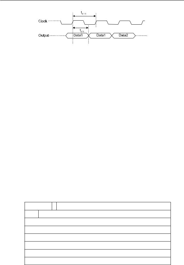
Figure 108. RMII Timing – Transmitting Data
Table 104. Timing Parameters – Transmitting Data
Timing Parameters |
Description |
Min |
Typ |
Max |
Unit |
tCY C |
Clock cycle |
20 |
20 |
20 |
ns |
tSU |
Setup time |
4 |
– |
– |
ns |
tH |
Hold time |
1 |
– |
– |
ns |
|
|
|
|
|
|
tOD |
Output delay |
6 |
9 |
12 |
ns |
10.7Ethernet DMA Features
The DMA has independent Transmit and Receive engines, and a CSR (Control and Status Registers) space. The Transmit engine transfers data from the system memory to the device port (MTL), while the Receive engine transmits data from the device port to the system memory. The controller uses descriptors to efficiently move data from source to destination with minimal Host CPU intervention. The DMA is designed for packet-oriented data transmission, such as frames in Ethernet. The controller can be programmed to interrupt the Host CPU for normal situations, such as the completion of frame transmission or reception, or when errors occur.
10.8Linked List Descriptors
This section shows the structure of the linked lists and the descriptors. Every linked list consists of eight words.
10.8.1 Transmit Descriptors
The structure of the transmitter linked lists is shown in Figure 10-9. Table 10-5 to Table 10-8 show the description of the linked lists.
TDES0
TDES1
TDES2
TDES3
TDES4
TDES5
TDES6
TDES7
31
OWN |
Ctrl[30:26] |
|
|
|
|
Ctrl [31:29]
Reserved
|
Reserved |
|
|
|
|
0 |
Ctrl[24:18] |
Status[16:7] |
Ctrl/status |
|
Status |
||
|
|
|||||
|
[6:3] |
|
[2:0] |
|||
|
|
|
|
|
||
|
|
|
|
|
|
|
Reserved |
|
|
Transmit Buffer Size[12:0] |
|
||
|
|
|
|
|
|
|
Buffer Address [31:0]
Next Descriptor Address[31:0]
Reserved
Reserved
Reserved
Reserved
Figure 109. Transmit Descriptor
Espressif Systems |
234 |
ESP32 TRM (Version 5.0) |
Submit Documentation Feedback

10 Ethernet Media Access Controller (MAC)
|
Table 105. Transmit Descriptor 0 (TDES0) |
||
|
|
|
|
Bits |
Name |
Description |
|
|
|
When set, this bit indicates that the descriptor is owned by the DMA. |
|
|
|
When this bit is reset, it indicates that the descriptor is owned by the |
|
|
|
Host. The DMA clears this bit, either when it completes the frame |
|
[31] |
OWN: Own Bit |
transmission or when the buffers allocated to the descriptor are |
|
empty. The ownership bit of the First Descriptor of the frame should |
|||
|
|
||
|
|
be set after all subsequent descriptors belonging to the same frame |
|
|
|
have been set. This avoids a possible race condition between fetch- |
|
|
|
ing a descriptor and the driver setting an ownership bit. |
|
|
|
|
|
|
|
When set, this bit sets the Transmit Interrupt (Register 5[0]) after the |
|
[30] |
IC: Interrupt on Completion |
present frame has been transmitted. This bit is valid only when the |
|
|
|
last segment bit (TDES0[29]) is set. |
|
|
|
|
|
|
|
When set, this bit indicates that the buffer contains the last segment |
|
[29] |
LS: Last Segment |
of the frame. When this bit is set, the TBS1 or TBS2 field in TDES1 |
|
|
|
should have a non-zero value. |
|
|
|
|
|
[28] |
FS: First Segment |
When set, this bit indicates that the buffer contains the first segment |
|
of a frame. |
|||
|
|
||
|
|
|
|
|
|
When this bit is set, the MAC does not append a cyclic redundancy |
|
[27] |
DC: Disable CRC |
check (CRC) to the end of the transmitted frame. This is valid only |
|
|
|
when the first segment (TDES0[28]) is set. |
|
|
|
|
|
|
|
When set, the MAC does not automatically add padding to a frame |
|
|
|
shorter than 64 bytes. When this bit is reset, the DMA automatically |
|
[26] |
DP: Disable Pad |
adds padding and CRC to a frame shorter than 64 bytes, and the |
|
|
|
CRC field is added despite the state of the DC (TDES0[27]) bit. This |
|
|
|
is valid only when the first segment (TDES0[28]) is set. |
|
|
|
|
|
[25] |
Reserved |
Reserved |
|
|
|
|
|
|
|
When set, the MAC replaces the last four bytes of the transmitted |
|
|
|
packet with recalculated CRC bytes. The host should ensure that |
|
[24] |
CRCR: CRC Replacement |
the CRC bytes are present in the frame being transmitted from the |
|
Control |
Transmit Buffer. This bit is valid when the First Segment control bit |
||
|
|||
|
|
(TDES0[28]) is set. In addition, CRC replacement is done only when |
|
|
|
Bit TDES0[27] is set to 1. |
|
|
|
|
|
Espressif Systems |
235 |
ESP32 TRM (Version 5.0) |
Submit Documentation Feedback

10 Ethernet Media Access Controller (MAC)
Bits |
Name |
Description |
|
|
|
These bits control the checksum calculation and insertion. The fol- |
|
|
|
lowing list describes the bit encoding: |
|
|
|
• 2’b00: Checksum insertion is disabled. |
|
|
|
• 2’b01: Only IP header checksum calculation and insertion are |
|
|
|
enabled. |
|
|
CIC: Checksum Insertion |
• 2’b10: IP header checksum and payload checksum calcula- |
|
[23:22] |
tion and insertion are enabled, but pseudo-header checksum |
||
Control |
|||
|
is not calculated in hardware. |
||
|
|
||
|
|
• 2’b11: IP Header checksum and payload checksum calcula- |
|
|
|
tion and insertion are enabled, and pseudo-header checksum |
|
|
|
is calculated in hardware. |
|
|
|
This field is valid when the First Segment control bit (TDES0[28]) is |
|
|
|
set. |
|
|
|
|
|
|
|
When set, this bit indicates that the descriptor list reached its final |
|
[21] |
TER: Transmit End of Ring |
descriptor. The DMA returns to the base address of the list, creating |
|
|
|
a Descriptor Ring. |
|
|
|
|
|
|
|
When set, this bit indicates that the second address in the descrip- |
|
|
TCH: Second Address |
tor is the Next Descriptor address, rather than the second buffer |
|
[20] |
address. When TDES0[20] is set, TBS2 (TDES1[28:16]) is a “don’t |
||
Chained |
|||
|
care” value. TDES0[21] takes precedence over TDES0[20]. This bit |
||
|
|
||
|
|
should be set to 1. |
|
|
|
|
|
|
|
When set, these bits request the MAC to perform VLAN tagging or |
|
|
|
untagging before transmitting the frames. If the frame is modified |
|
|
|
for VLAN tags, the MAC automatically recalculates and replaces the |
|
|
|
CRC bytes. The following list describes the values of these bits: |
|
|
|
• 2’b00: Do not add a VLAN tag. |
|
|
VLIC: VLAN Insertion |
• 2’b01: Remove the VLAN tag from the frames before trans- |
|
[19:18] |
mission. This option should be used only with the VLAN |
||
Control |
|||
|
frames. |
||
|
|
||
|
|
• 2’b10: Insert a VLAN tag with the tag value programmed in |
|
|
|
VLAN Tag Inclusion or Replacement Register. |
|
|
|
• 2’b1: Replace the VLAN tag in frames with the Tag value |
|
|
|
programmed in VLAN Tag Inclusion or Replacement Regis- |
|
|
|
ter. This option should be used only with the VLAN frames. |
|
|
|
|
|
[17] |
Reserved |
Reserved |
|
|
|
|
Espressif Systems |
236 |
ESP32 TRM (Version 5.0) |
Submit Documentation Feedback

10 Ethernet Media Access Controller (MAC)
Bits |
Name |
Description |
|
|
|
When set, this bit indicates that the MAC transmitter detected an |
|
|
|
error in the IP datagram header. The transmitter checks the header |
|
|
|
length in the IPv4 packet against the number of header bytes re- |
|
|
|
ceived from the application, and indicates an error status if there |
|
[16] |
IHE: IP Header Error |
is a mismatch. For IPv6 frames, a header error is reported if the |
|
main header length is not 40 bytes. Furthermore, the Ethernet |
|||
|
|
||
|
|
Length/Type field value for an IPv4 or IPv6 frame must match the IP |
|
|
|
header version received with the packet. For IPv4 frames, an error |
|
|
|
status is also indicated if the Header Length field has a value less |
|
|
|
than 0x5. |
|
|
|
|
|
|
|
Indicates the logical OR of the following bits: |
|
|
|
• TDES0[14]: Jabber Timeout |
|
|
|
• TDES0[13]: Frame Flush |
|
|
|
• TDES0[11]: Loss of Carrier |
|
|
|
• TDES0[10]: No Carrier |
|
[15] |
ES: Error Summary |
• TDES0[9]: Late Collision |
|
|
|
• TDES0[8]: Excessive Collision |
|
|
|
• TDES0[2]: Excessive Deferral |
|
|
|
• TDES0[1]: Underflow Error |
|
|
|
• TDES0[16]: IP Header Error |
|
|
|
• TDES0[12]: IP Payload Error |
|
|
|
|
|
|
|
When set, this bit indicates the MAC transmitter has experienced a |
|
[14] |
JT: Jabber Timeout |
jabber timeout. This bit is only set when EMACCONFIG_REG’s bit |
|
|
|
EMACJABBER is not set. |
|
|
|
|
|
[13] |
FF: Frame Flushed |
When set, this bit indicates that the DMA or MTL flushed the frame |
|
because of a software Flush command given by the CPU. |
|||
|
|
||
|
|
|
Espressif Systems |
237 |
ESP32 TRM (Version 5.0) |
Submit Documentation Feedback

10 Ethernet Media Access Controller (MAC)
Bits |
Name |
Description |
|
|
|
When set, this bit indicates that MAC transmitter detected an error |
|
|
|
in the TCP, UDP, or ICMP IP datagram payload. |
|
[12] |
IPE: IP Payload Error |
The transmitter checks the payload length received in the IPv4 or |
|
IPv6 header against the actual number of TCP, UDP, or ICMP packet |
|||
|
|
||
|
|
bytes received from the application, and issues an error status in |
|
|
|
case of a mismatch. |
|
|
|
|
|
|
|
When set, this bit indicates that a loss of carrier occurred during |
|
|
|
frame transmission (that is, the MII_CRS signal was inactive for one |
|
[11] |
LOC: Loss of Carrier |
or more transmit clock periods during frame transmission). This is |
|
|
|
valid only for the frames transmitted without collision when the MAC |
|
|
|
operates in the half-duplex mode. |
|
|
|
|
|
[10] |
NC: No Carrier |
When set, this bit indicates that the Carrier Sense signal from the |
|
PHY was not asserted during transmission. |
|||
|
|
||
|
|
|
|
|
|
When set, this bit indicates that frame transmission is aborted be- |
|
|
|
cause of a collision occurring after the collision window (64 byte- |
|
[9] |
LC: Late Collision |
times including Preamble in MII mode, and 512 byte-times including |
|
|
|
Preamble and Carrier Extension). This bit is not valid if the Under- |
|
|
|
flow Error bit is set. |
|
|
|
|
|
|
|
When set, this bit indicates that the transmission was aborted after |
|
|
|
16 successive collisions while attempting to transmit the current |
|
[8] |
EC: Excessive Collision |
frame. If bit EMACRETRY of EMACCONFIG_REG is set, this bit |
|
|
|
is set after the first collision, and the transmission of the frame is |
|
|
|
aborted. |
|
|
|
|
|
[7] |
VF: VLAN Frame |
When set, this bit indicates that the transmitted frame is a VLAN- |
|
type frame. |
|||
|
|
||
|
|
|
|
|
|
These status bits indicate the number of collisions that occurred |
|
[6:3] |
Ctrl/status |
before the frame was transmitted. This count is not valid when the |
|
Excessive Collisions bit (TDES0[8]) is set. The core updates this |
|||
|
|
||
|
|
status field only in the half-duplex mode. |
|
|
|
|
|
|
|
When set, this bit indicates that the transmission has ended be- |
|
[2] |
ED: Excessive Deferral |
cause of excessive deferral of over 24,288 bit times (if Jumbo Frame |
|
is enabled) if bit EMACDEFERRAL of EMACCONFIG_REG is set |
|||
|
|
||
|
|
high. |
|
|
|
|
|
|
|
When set, this bit indicates that the MAC aborted the frame be- |
|
|
|
cause the data arrived late from the Host memory. Underflow Er- |
|
|
|
ror indicates that the DMA encountered an empty transmit buffer |
|
[1] |
UF: Underflow Error |
while transmitting the frame. The transmission process enters the |
|
|
|
Suspended state and sets both Bit[5] in Transmit Underflow Regis- |
|
|
|
ter (Status Register) and Bit[0] in Transmit Interrupt Register (Status |
|
|
|
Register). |
|
|
|
|
|
|
|
When set, this bit indicates that the MAC defers before transmission |
|
[0] |
DB: Deferred Bit |
because of the presence of a carrier. This bit is valid only in the half- |
|
|
|
duplex mode. |
|
|
|
|
Espressif Systems |
238 |
ESP32 TRM (Version 5.0) |
Submit Documentation Feedback