

- •1 System and Memory
- •1.1 Introduction
- •1.2 Features
- •1.3 Functional Description
- •1.3.1 Address Mapping
- •1.3.2 Embedded Memory
- •1.3.3 External Memory
- •1.3.5 Peripherals
- •2 Interrupt Matrix (INTERRUPT)
- •2.1 Overview
- •2.2 Features
- •2.3 Functional Description
- •2.3.1 Peripheral Interrupt Source
- •2.3.2 CPU Interrupt
- •2.3.3 Allocate Peripheral Interrupt Sources to Peripheral Interrupt on CPU
- •2.3.4 CPU NMI Interrupt Mask
- •2.3.5 Query Current Interrupt Status of Peripheral Interrupt Source
- •2.4 Registers
- •3 Reset and Clock
- •3.1 System Reset
- •3.1.1 Introduction
- •3.1.2 Reset Source
- •3.2 System Clock
- •3.2.1 Introduction
- •3.2.3 CPU Clock
- •3.2.4 Peripheral Clock
- •3.2.7 Audio PLL
- •3.3 Register Summary
- •3.4 Registers
- •4.1 Overview
- •4.2 Peripheral Input via GPIO Matrix
- •4.2.1 Summary
- •4.2.2 Functional Description
- •4.2.3 Simple GPIO Input
- •4.3 Peripheral Output via GPIO Matrix
- •4.3.1 Summary
- •4.3.3 Simple GPIO Output
- •4.4 Direct I/O via IO_MUX
- •4.4.1 Summary
- •4.4.2 Functional Description
- •4.5 RTC IO_MUX for Low Power and Analog I/O
- •4.5.1 Summary
- •4.5.2 Analog Function Description
- •4.7 Pad Hold Feature
- •4.8 I/O Pad Power Supplies
- •4.8.1 VDD_SDIO Power Domain
- •4.9 Peripheral Signal List
- •4.10 IO_MUX Pad List
- •4.11 RTC_MUX Pin List
- •4.12 Register Summary
- •4.12.1 GPIO Matrix Register Summary
- •4.12.2 IO MUX Register Summary
- •4.12.3 RTC IO MUX Register Summary
- •4.13 Registers
- •4.13.1 GPIO Matrix Registers
- •4.13.2 IO MUX Registers
- •4.13.3 RTC IO MUX Registers
- •5 DPort Registers
- •5.1 Introduction
- •5.2 Features
- •5.3 Functional Description
- •5.3.1 System and Memory Register
- •5.3.2 Reset and Clock Registers
- •5.3.3 Interrupt Matrix Register
- •5.3.4 DMA Registers
- •5.3.5 MPU/MMU Registers
- •5.3.7 Peripheral Clock Gating and Reset
- •5.4 Register Summary
- •5.5 Registers
- •6 DMA Controller (DMA)
- •6.1 Overview
- •6.2 Features
- •6.3 Functional Description
- •6.3.1 DMA Engine Architecture
- •6.3.2 Linked List
- •6.4 UART DMA (UDMA)
- •7 SPI Controller (SPI)
- •7.1 Overview
- •7.5 Parallel QSPI
- •7.5.1 Communication Format of Parallel QSPI
- •7.6.1 SPI Interrupts
- •7.6.2 DMA Interrupts
- •7.7 Register Summary
- •7.8 Registers
- •8 SDIO Slave Controller
- •8.1 Overview
- •8.2 Features
- •8.3 Functional Description
- •8.3.1 SDIO Slave Block Diagram
- •8.3.3 Register Access
- •8.3.6 SDIO Bus Timing
- •8.3.7 Interrupt
- •8.4 Register Summary
- •8.5 SLC Registers
- •8.6 SLC Host Registers
- •8.7 HINF Registers
- •9 SD/MMC Host Controller
- •9.1 Overview
- •9.2 Features
- •9.3 SD/MMC External Interface Signals
- •9.4 Functional Description
- •9.4.1 SD/MMC Host Controller Architecture
- •9.4.2 Command Path
- •9.4.3 Data Path
- •9.5 Software Restrictions for Proper CIU Operation
- •9.6 RAM for Receiving and Sending Data
- •9.6.1 Transmit RAM Module
- •9.6.2 Receive RAM Module
- •9.8 The Structure of a Linked List
- •9.9 Initialization
- •9.9.1 DMAC Initialization
- •9.9.2 DMAC Transmission Initialization
- •9.9.3 DMAC Reception Initialization
- •9.11 Interrupt
- •9.12 Register Summary
- •9.13 Registers
- •10 Ethernet Media Access Controller (MAC)
- •10.1 Overview
- •10.2 EMAC_CORE
- •10.2.1 Transmit Operation
- •10.2.2 Receive Operation
- •10.3 MAC Interrupt Controller
- •10.4 MAC Address Filtering
- •10.4.1 Unicast Destination Address Filtering
- •10.4.2 Multicast Destination Address Filtering
- •10.4.3 Broadcast Address Filtering
- •10.4.4 Unicast Source Address Filtering
- •10.4.5 Inverse Filtering Operation
- •10.4.6 Good Transmitted Frames and Received Frames
- •10.5 EMAC_MTL (MAC Transaction Layer)
- •10.6 PHY Interface
- •10.6.1 MII (Media Independent Interface)
- •10.6.3 Station Management Agent (SMA) Interface
- •10.6.4 RMII Timing
- •10.7 Ethernet DMA Features
- •10.8 Linked List Descriptors
- •10.8.1 Transmit Descriptors
- •10.8.2 Receive Descriptors
- •10.9 Register Summary
- •10.10 Registers
- •11 I2C Controller (I2C)
- •11.1 Overview
- •11.2 Features
- •11.3 Functional Description
- •11.3.1 Introduction
- •11.3.2 Architecture
- •11.3.3 I2C Bus Timing
- •11.3.7 Interrupts
- •11.4 Register Summary
- •11.5 Registers
- •12 I2S Controller (I2S)
- •12.1 Overview
- •12.2 Features
- •12.3 The Clock of I2S Module
- •12.4 I2S Mode
- •12.4.1 Supported Audio Standards
- •12.4.2 Module Reset
- •12.4.3 FIFO Operation
- •12.4.5 Receiving Data
- •12.5.1 LCD Master Transmitting Mode
- •12.5.2 Camera Slave Receiving Mode
- •12.5.3 ADC/DAC mode
- •12.6 I2S Interrupts
- •12.6.1 FIFO Interrupts
- •12.6.2 DMA Interrupts
- •12.7 Register Summary
- •12.8 Registers
- •13 UART Controller (UART)
- •13.1 Overview
- •13.2 UART Features
- •13.3 Functional Description
- •13.3.1 Introduction
- •13.3.3 UART RAM
- •13.3.5 UART Data Frame
- •13.3.7 Flow Control
- •13.3.8 UART DMA
- •13.3.9 UART Interrupts
- •13.3.10 UHCI Interrupts
- •13.4 Register Summary
- •13.4.1 UART Register Summary
- •13.5 Registers
- •13.5.1 UART Registers
- •13.5.2 UHCI Registers
- •14 LED PWM Controller (LEDC)
- •14.1 Introduction
- •14.2 Functional Description
- •14.2.1 Architecture
- •14.2.3 Channels
- •14.2.4 Interrupts
- •14.3 Register Summary
- •14.4 Registers
- •15 Remote Control Peripheral (RMT)
- •15.1 Introduction
- •15.2 Functional Description
- •15.2.1 RMT Architecture
- •15.2.3 Clock
- •15.2.4 Transmitter
- •15.2.5 Receiver
- •15.2.6 Interrupts
- •15.3 Register Summary
- •15.4 Registers
- •16 Motor Control PWM (PWM)
- •16.1 Introduction
- •16.2 Features
- •16.3 Submodules
- •16.3.1 Overview
- •16.3.2 PWM Timer Submodule
- •16.3.3 PWM Operator Submodule
- •16.3.4 Capture Submodule
- •16.4 Register Summary
- •16.5 Registers
- •17 Pulse Count Controller (PCNT)
- •17.1 Overview
- •17.2 Functional Description
- •17.2.1 Architecture
- •17.2.2 Counter Channel Inputs
- •17.2.3 Watchpoints
- •17.2.4 Examples
- •17.2.5 Interrupts
- •18 Timer Group (TIMG)
- •18.1 Introduction
- •18.2 Functional Description
- •18.2.2 64-bit Time-base Counter
- •18.2.3 Alarm Generation
- •18.2.4 MWDT
- •18.2.5 Interrupts
- •18.3 Register Summary
- •18.4 Registers
- •19 Watchdog Timers (WDT)
- •19.1 Introduction
- •19.2 Features
- •19.3 Functional Description
- •19.3.1 Clock
- •20 eFuse Controller
- •20.1 Introduction
- •20.2 Features
- •20.3 Functional Description
- •20.3.1 Structure
- •20.3.3 Software Reading of System Parameters
- •20.3.4 The Use of System Parameters by Hardware Modules
- •20.3.5 Interrupts
- •20.4 Register Summary
- •20.5 Registers
- •21 Two-wire Automotive Interface (TWAI)
- •21.1 Overview
- •21.2 Features
- •21.3 Functional Protocol
- •21.3.1 TWAI Properties
- •21.3.2 TWAI Messages
- •21.3.3 TWAI Errors
- •21.3.4 TWAI Bit Timing
- •21.4 Architectural Overview
- •21.4.1 Registers Block
- •21.4.2 Bit Stream Processor
- •21.4.3 Error Management Logic
- •21.4.4 Bit Timing Logic
- •21.4.5 Acceptance Filter
- •21.5 Functional Description
- •21.5.1 Modes
- •21.5.2 Bit Timing
- •21.5.3 Interrupt Management
- •21.5.4 Transmit and Receive Buffers
- •21.5.5 Receive FIFO and Data Overruns
- •21.5.6 Acceptance Filter
- •21.5.8 Error Code Capture
- •21.5.9 Arbitration Lost Capture
- •21.6 Register Summary
- •21.7 Registers
- •22 AES Accelerator (AES)
- •22.1 Introduction
- •22.2 Features
- •22.3 Functional Description
- •22.3.1 AES Algorithm Operations
- •22.3.2 Key, Plaintext and Ciphertext
- •22.3.3 Endianness
- •22.3.4 Encryption and Decryption Operations
- •22.3.5 Speed
- •22.4 Register Summary
- •22.5 Registers
- •23 SHA Accelerator (SHA)
- •23.1 Introduction
- •23.2 Features
- •23.3 Functional Description
- •23.3.1 Padding and Parsing the Message
- •23.3.2 Message Digest
- •23.3.3 Hash Operation
- •23.3.4 Speed
- •23.4 Register Summary
- •23.5 Registers
- •24 RSA Accelerator (RSA)
- •24.1 Introduction
- •24.2 Features
- •24.3 Functional Description
- •24.3.1 Initialization
- •24.3.2 Large Number Modular Exponentiation
- •24.3.4 Large Number Multiplication
- •24.4 Register Summary
- •24.5 Registers
- •25 Random Number Generator (RNG)
- •25.1 Introduction
- •25.2 Feature
- •25.3 Functional Description
- •25.5 Register Summary
- •25.6 Register
- •26 External Memory Encryption and Decryption (FLASH)
- •26.1 Overview
- •26.2 Features
- •26.3 Functional Description
- •26.3.1 Key Generator
- •26.3.2 Flash Encryption Block
- •26.3.3 Flash Decryption Block
- •26.4 Register Summary
- •26.5 Register
- •27 Memory Management and Protection Units (MMU, MPU)
- •27.1 Introduction
- •27.2 Features
- •27.3 Functional Description
- •27.3.1 PID Controller
- •28 Process ID Controller (PID)
- •28.1 Overview
- •28.2 Features
- •28.3 Functional Description
- •28.3.1 Interrupt Identification
- •28.3.2 Information Recording
- •28.3.3 Proactive Process Switching
- •28.4 Register Summary
- •28.5 Registers
- •29 On-Chip Sensors and Analog Signal Processing
- •29.1 Introduction
- •29.2 Capacitive Touch Sensor
- •29.2.1 Introduction
- •29.2.2 Features
- •29.2.3 Available GPIOs
- •29.2.4 Functional Description
- •29.2.5 Touch FSM
- •29.3.1 Introduction
- •29.3.2 Features
- •29.3.3 Outline of Function
- •29.3.4 RTC SAR ADC Controllers
- •29.3.5 DIG SAR ADC Controllers
- •29.4.1 Introduction
- •29.4.2 Features
- •29.4.4 Cosine Waveform Generator
- •29.5 Register Summary
- •29.5.1 Sensors
- •29.5.2 Advanced Peripheral Bus
- •29.6 Registers
- •29.6.1 Sensors
- •29.6.2 Advanced Peripheral Bus
- •30 ULP Coprocessor (ULP)
- •30.1 Introduction
- •30.2 Features
- •30.4 Instruction Set
- •30.4.2 ST – Store Data in Memory
- •30.4.3 LD – Load Data from Memory
- •30.4.4 JUMP – Jump to an Absolute Address
- •30.4.5 JUMPR – Jump to a Relative Offset (Conditional upon R0)
- •30.4.7 HALT – End the Program
- •30.4.8 WAKE – Wake up the Chip
- •30.4.10 WAIT – Wait for a Number of Cycles
- •30.4.12 I2C_RD/I2C_WR – Read/Write I²C
- •30.4.13 REG_RD – Read from Peripheral Register
- •30.5 ULP Program Execution
- •30.6 RTC_I2C Controller
- •30.6.1 Configuring RTC_I2C
- •30.6.2 Using RTC_I2C
- •30.7 Register Summary
- •30.7.1 SENS_ULP Address Space
- •30.7.2 RTC_I2C Address Space
- •30.8 Registers
- •30.8.1 SENS_ULP Address Space
- •30.8.2 RTC_I2C Address Space
- •31 Low-Power Management (RTC_CNTL)
- •31.1 Introduction
- •31.2 Features
- •31.3 Functional Description
- •31.3.2 Digital Core Voltage Regulator
- •31.3.4 Flash Voltage Regulator
- •31.3.5 Brownout Detector
- •31.3.6 RTC Module
- •31.3.9 Predefined Power Modes
- •31.3.10 Wakeup Source
- •31.3.12 RTC Timer
- •31.3.13 RTC Boot
- •31.4 Register Summary
- •31.5 Registers
- •Glossary
- •Abbreviations for Peripherals
- •Abbreviations for Registers
- •Revision History

10Ethernet Media Access Controller (MAC)
•Jabber timeout
•No carrier or loss of carrier
•Late collision
•Frame underflow
•Excessive deferral
•Excessive collision
The received frames are considered ”good frames”, if there are not any of the following errors:
•CRC error
•Runt frames (frames shorter than 64 bytes)
•Alignment error (in 10/100 Mbps modes only)
•Length error (non-type frames only)
•Frame size over the maximum size (for non-type frames over the maximum frame size only)
•MII_RXER input error
The maximum frame size depends on the frame type:
•The maximum size of untagged frames = 1518 bytes
•The maximum size of VLAN frames = 1522 bytes
10.5EMAC_MTL (MAC Transaction Layer)
The MAC Transaction Layer provides FIFO memory to buffer and regulates the frames between the application system memory and the MAC. It also enables the data to be transmitted between the application clock domain and the MAC clock domains. The MTL layer has two data paths, namely the Transmit path and the Receive path. The data path for both directions is 32-bit wide and operates with a simple FIFO protocol.
10.6PHY Interface
The DMA and the Host driver communicate through two data structures:
•Control and Status Registers (CSR)
•Descriptor lists and data buffers
For details please refer to Register Summary and Linked List Descriptors.
10.6.1 MII (Media Independent Interface)
Media Independent Interface (MII) defines the interconnection between MAC sublayers and PHYs at the data transmission rate of 10 Mbit/s and 100 Mbit/s.
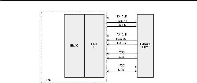
10.6.1.1 Interface Signals Between MII and PHY
Interface signals between MII and PHY are shown in Figure 10-3.
Espressif Systems |
229 |
ESP32 TRM (Version 5.0) |
Submit Documentation Feedback
10 Ethernet Media Access Controller (MAC)
Figure 103. MII Interface
MII Interface Signal Description:
•MII_TX_CLK: TX clock signal. This signal provides the reference timing for TX data transmission. The frequencies are divided into two types: 2.5 MHz at a data transmission rate of 10 Mbit/s, and 25 MHz at 100 Mbit/s.
•MII_TXD[3:0]: Transmit data signal in groups of four, syn-driven by the MAC sub-layer, and valid only when the MII_TX_EN signal is valid. MII_TXD[0] is the lowest significant bit and MII_TXD[3] is the highest significant bit. When the signal MII_TX_EN is pulled low, sending data does not have any effect on the PHY.
•MII_TX_EN: Transmit data enable signal. This signal indicates that the MAC is currently sending nibbles (4 bits) for the MII. This signal must be synchronized with the first nibble of the header (MII_TX_CLK) and must be synchronized when all nibbles to be transmitted are sent to the MII.
•MII_RX_CLK: RX clock signal. This signal provides the reference timing for RX data transmission. The frequencies are divided into two types: 2.5 MHz at the data transmission rate of 10 Mbit/s, and 25 MHz at 100 Mbit/s.
•MII_RXD[3:0]: Receive data signal in groups of four, syn-driven by the PHY, and valid only when MII_RX_DV signal is valid. MII_RXD[0] is the lowest significant bit and MII_RXD[3] is the highest significant bit. When MII_RX_DV is disabled and MII_RX_ER is enabled, the specific MII_RXD[3:0] value represents specific information from the PHY.
•MII_RX_DV: Receive data valid signal. This signal indicates that the PHY is currently receiving the recovered and decoded nibble that will be transmitted to the MII. This signal must be synchronized with the first nibble of the recovered frame (MII_RX_CLK) and remain synchronized till the last nibble of the recovered frame. This signal must be disabled before the first clock cycle following the last nibble. In order to receive the frame correctly, the MII_RX_DV signal must cover the frame to be received over the time range, starting no later than when the SFD field appears.
•MII_CRS: Carrier sense signal. When the transmitting or receiving medium is in the non-idle state, the signal is enabled by the PHY. When the transmitting or receiving medium is in the idle state, the signal is disabled by the PHY. The PHY must ensure that the MII_CRS signal remains valid under conflicting conditions. This signal does not need to be synchronized with the TX and RX clocks. In full-duplex mode, this signal is insignificant.
•MII_COL: Collision detection signal. After a collision is detected on the medium, the PHY must immedi-
Espressif Systems |
230 |
ESP32 TRM (Version 5.0) |
Submit Documentation Feedback
10 Ethernet Media Access Controller (MAC)
ately enable the collision detection signal, and the collision detection signal must remain active as long as a condition for collision exists. This signal does not need to be synchronized with the TX and RX clocks. In full-duplex mode, this signal is meaningless.
•MII_RX_ER: Receive error signal. The signal must remain for one or more cycles (MII_RX_CLK) to indicate to the MAC sublayer that an error has been detected somewhere in the frame.
•MDIO and MDC: Management Data Input/Output and Management Data Clock. The two signals constitute a serial bus defined for the Ethernet family of IEEE 802.3 standards, used to transfer control and data information to the PHY, see section Station Management Agent (SMA) Interface.
10.6.1.2 MII Clock
In MII mode, there are two directions of clock, Tx and Rx clocks in the interface between MII and the PHY. MII_TX_CLK is used to synchronize the TX data, and MII_RX_CLK is used to synchronize the RX data. The MII_RX_CLK clock is provided by the PHY. The MII_TX_CLK is provided by the chip’s internal PLL or external crystal oscillator. For details regarding Figure 10-4, please refer to the clock-related registers in Register Summary.
Figure 104. MII Clock
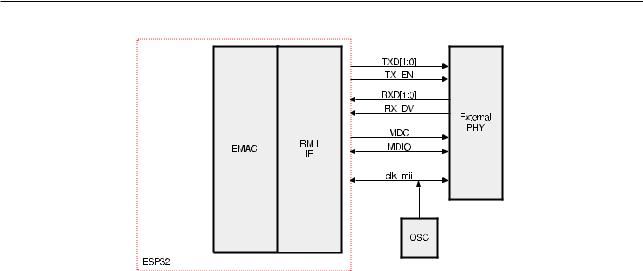
10.6.2 RMII (Reduced MediaIndependent Interface)
RMII interface signals are shown in figure 10-5.
Espressif Systems |
231 |
ESP32 TRM (Version 5.0) |
Submit Documentation Feedback
10 Ethernet Media Access Controller (MAC)
Figure 105. RMII Interface
10.6.2.1 RMII Interface Signal Description
The Reduced Media-Independent Interface (RMII) specification reduces the number of pins between the microcontroller’s external peripherals and the external PHY at a data transmission rate of 10 Mbit/s or 100 Mbit/s. According to the IEEE 802.3u standard, MII includes 16 pins that contain data and control signals. The RMII specification reduces 62.5% of the pins to the number of seven.
RMII has the following features:
•Support for an operating rate of 10 Mbit/s or 100 Mbit/s
•The reference clock frequency must be 50 MHz.
•The same reference clock must be provided externally both to the MAC and the external Ethernet PHY. It provides independent 2-bit-wide Tx and Rx data paths.
10.6.2.2 RMII Clock
The configuration of the RMII clock is as figure 10-6 shows.
Espressif Systems |
232 |
ESP32 TRM (Version 5.0) |
Submit Documentation Feedback