

2Interrupt Matrix (INTERRUPT)
2Interrupt Matrix (INTERRUPT)
2.1Overview
The Interrupt Matrix embedded in the ESP32 independently allocates peripheral interrupt sources to the two CPUs’ peripheral interrupts. This configuration is made to be highly flexible in order to meet many different needs.
2.2Features
•Accepts 71 peripheral interrupt sources as input.
•Generates 26 peripheral interrupt sources per CPU as output (52 total).
•CPU NMI Interrupt Mask.
•Queries current interrupt status of peripheral interrupt sources.
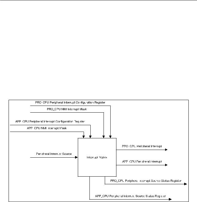
The structure of the Interrupt Matrix is shown in Figure 2-1.
Figure 21. Interrupt Matrix Structure
2.3Functional Description
2.3.1Peripheral Interrupt Source
ESP32 has 71 peripheral interrupt sources in total. All peripheral interrupt sources are listed in table 2-1. 67 of 71 ESP32 peripheral interrupt sources can be allocated to either CPU.
The four remaining peripheral interrupt sources are CPU-specific, two per CPU. GPIO_INTERRUPT_PRO and GPIO_INTERRUPT_PRO_NMI can only be allocated to PRO_CPU. GPIO_INTERRUPT_APP and GPIO_INTERRUPT _APP_NMI can only be allocated to APP_CPU. As a result, PRO_CPU and APP_CPU each have 69 peripheral interrupt sources.
Espressif Systems |
34 |
ESP32 TRM (Version 5.0) |
Submit Documentation Feedback

Systems Espressif
Documentation Submit |
35 |
Feedback |
|
0).5 (Version TRM ESP32
Table 21. PRO_CPU, APP_CPU Interrupt Configuration
|
|
|
|
PRO_CPU |
|
|
|
|
|
APP_CPU |
|
|
|
|
|
|
|
|
|
|
|
Peripheral Interrupt Source |
|
|
|
|
|
|
|||
|
Peripheral Interrupt |
|
|
Status Register |
|
|
Status Register |
|
|
Peripheral Interrupt |
|
||||
|
Configuration Register |
|
|
No. |
Name |
|
No. |
|
|
Configuration Register |
|
||||
|
|
|
Bit |
Name |
|
|
|
|
|
Name |
Bit |
|
|
|
|
|
|
|
|
|
|
|
|
|
|
|
|||||
DPORT_PRO_MAC_INTR_MAP_REG |
0 |
|
0 |
MAC_INTR |
0 |
|
0 |
DPORT_APP_MAC_INTR_MAP_REG |
|||||||
|
|
|
|
|
|
|
|
|
|||||||
DPORT_PRO_MAC_NMI_MAP_REG |
1 |
|
1 |
MAC_NMI |
1 |
|
1 |
DPORT_APP_MAC_NMI_MAP_REG |
|||||||
DPORT_PRO_BB_INT_MAP_REG |
2 |
|
2 |
BB_INT |
2 |
|
2 |
DPORT_APP_BB_INT_MAP_REG |
|||||||
|
|
|
|
|
|
|
|
|
|||||||
DPORT_PRO_BT_MAC_INT_MAP_REG |
3 |
|
3 |
BT_MAC_INT |
3 |
|
3 |
DPORT_APP_BT_MAC_INT_MAP_REG |
|||||||
|
|
|
|
|
|
|
|
|
|||||||
DPORT_PRO_BT_BB_INT_MAP_REG |
4 |
|
4 |
BT_BB_INT |
4 |
|
4 |
DPORT_APP_BT_BB_INT_MAP_REG |
|||||||
DPORT_PRO_BT_BB_NMI_MAP_REG |
5 |
|
5 |
BT_BB_NMI |
5 |
|
5 |
DPORT_APP_BT_BB_NMI_MAP_REG |
|||||||
|
|
|
|
|
|
|
|
|
|||||||
DPORT_PRO_RWBT_IRQ_MAP_REG |
6 |
|
6 |
RWBT_IRQ |
6 |
|
6 |
DPORT_APP_RWBT_IRQ_MAP_REG |
|||||||
|
|
|
|
|
|
|
|
|
|||||||
DPORT_PRO_RWBLE_IRQ_MAP_REG |
7 |
|
7 |
RWBLE_IRQ |
7 |
|
7 |
DPORT_APP_RWBLE_IRQ_MAP_REG |
|||||||
|
|
|
|
|
|
|
|
|
|||||||
DPORT_PRO_RWBT_NMI_MAP_REG |
8 |
|
8 |
RWBT_NMI |
8 |
|
8 |
DPORT_APP_RWBT_NMI_MAP_REG |
|||||||
|
|
|
|
|
|
|
|
|
|||||||
DPORT_PRO_RWBLE_NMI_MAP_REG |
9 |
|
9 |
RWBLE_NMI |
9 |
|
9 |
DPORT_APP_RWBLE_NMI_MAP_REG |
|||||||
DPORT_PRO_SLC0_INTR_MAP_REG |
10 |
|
10 |
SLC0_INTR |
10 |
|
10 |
DPORT_APP_SLC0_INTR_MAP_REG |
|||||||
|
|
|
|
|
|
|
|
|
|||||||
DPORT_PRO_SLC1_INTR_MAP_REG |
11 |
|
11 |
SLC1_INTR |
11 |
|
11 |
DPORT_APP_SLC1_INTR_MAP_REG |
|||||||
|
|
|
|
|
|
|
|
|
|||||||
DPORT_PRO_UHCI0_INTR_MAP_REG |
12 |
|
12 |
UHCI0_INTR |
12 |
|
12 |
DPORT_APP_UHCI0_INTR_MAP_REG |
|||||||
DPORT_PRO_UHCI1_INTR_MAP_REG |
13 |
|
13 |
UHCI1_INTR |
13 |
|
13 |
DPORT_APP_UHCI1_INTR_MAP_REG |
|||||||
|
|
|
|
|
|
|
|
|
|||||||
DPORT_PRO_TG_T0_LEVEL_INT_MAP_REG |
14 |
|
14 |
TG_T0_LEVEL_INT |
14 |
|
14 |
DPORT_APP_TG_T0_LEVEL_INT_MAP_REG |
|||||||
|
|
|
|
|
|
|
|
|
|||||||
DPORT_PRO_TG_T1_LEVEL_INT_MAP_REG |
15 |
DPORT_PRO_INTR_STATUS_REG_0_REG |
15 |
TG_T1_LEVEL_INT |
15 |
DPORT_APP_INTR_STATUS_REG_0_REG |
15 |
DPORT_APP_TG_T1_LEVEL_INT_MAP_REG |
|||||||
DPORT_PRO_TG_WDT_LEVEL_INT_MAP_REG |
16 |
16 |
TG_WDT_LEVEL_INT |
16 |
16 |
DPORT_APP_TG_WDT_LEVEL_INT_MAP_REG |
|||||||||
|
|
||||||||||||||
|
|
|
|
|
|
|
|
|
|||||||
DPORT_PRO_TG_LACT_LEVEL_INT_MAP_REG |
17 |
|
17 |
TG_LACT_LEVEL_INT |
17 |
|
17 |
DPORT_APP_TG_LACT_LEVEL_INT_MAP_REG |
|||||||
|
|
|
|
|
|
|
|
|
|||||||
DPORT_PRO_TG1_T0_LEVEL_INT_MAP_REG |
18 |
|
18 |
TG1_T0_LEVEL_INT |
18 |
|
18 |
DPORT_APP_TG1_T0_LEVEL_INT_MAP_REG |
|||||||
|
|
|
|
|
|
|
|
|
|||||||
DPORT_PRO_TG1_T1_LEVEL_INT_MAP_REG |
19 |
|
19 |
TG1_T1_LEVEL_INT |
19 |
|
19 |
DPORT_APP_TG1_T1_LEVEL_INT_MAP_REG |
|||||||
|
|
|
|
|
|
|
|
|
|||||||
DPORT_PRO_TG1_WDT_LEVEL_INT_MAP_REG |
20 |
|
20 |
TG1_WDT_LEVEL_INT |
20 |
|
20 |
DPORT_APP_TG1_WDT_LEVEL_INT_MAP_REG |
|||||||
|
|
|
|
|
|
|
|
|
|||||||
DPORT_PRO_TG1_LACT_LEVEL_INT_MAP_REG |
21 |
|
21 |
TG1_LACT_LEVEL_INT |
21 |
|
21 |
DPORT_APP_TG1_LACT_LEVEL_INT_MAP_REG |
|||||||
|
|
|
|
|
|
|
|
|
|
||||||
DPORT_PRO_GPIO_INTERRUPT_MAP_REG |
22 |
|
22 |
GPIO_INTERRUPT_PRO |
|
GPIO_INTERRUPT_APP |
22 |
|
22 |
DPORT_APP_GPIO_INTERRUPT_MAP_REG |
|||||
DPORT_PRO_GPIO_INTERRUPT_NMI_MAP_REG |
23 |
|
23 |
GPIO_INTERRUPT_PRO_NMI |
|
GPIO_INTERRUPT_APP_NMI |
23 |
|
23 |
DPORT_APP_GPIO_INTERRUPT_NMI_MAP_REG |
|||||
DPORT_PRO_CPU_INTR_FROM_CPU_0_MAP_REG |
24 |
|
24 |
CPU_INTR_FROM_CPU_0 |
24 |
|
24 |
DPORT_APP_CPU_INTR_FROM_CPU_0_MAP_REG |
|||||||
|
|
|
|
|
|
|
|
|
|||||||
DPORT_PRO_CPU_INTR_FROM_CPU_1_MAP_REG |
25 |
|
25 |
CPU_INTR_FROM_CPU_1 |
25 |
|
25 |
DPORT_APP_CPU_INTR_FROM_CPU_1_MAP_REG |
|||||||
|
|
|
|
|
|
|
|
|
|||||||
DPORT_PRO_CPU_INTR_FROM_CPU_2_MAP_REG |
26 |
|
26 |
CPU_INTR_FROM_CPU_2 |
26 |
|
26 |
DPORT_APP_CPU_INTR_FROM_CPU_2_MAP_REG |
|||||||
|
|
|
|
|
|
|
|
|
|||||||
DPORT_PRO_CPU_INTR_FROM_CPU_3_MAP_REG |
27 |
|
27 |
CPU_INTR_FROM_CPU_3 |
27 |
|
27 |
DPORT_APP_CPU_INTR_FROM_CPU_3_MAP_REG |
|||||||
|
|
|
|
|
|
|
|
|
|||||||
DPORT_PRO_SPI_INTR_0_MAP_REG |
28 |
|
28 |
SPI_INTR_0 |
28 |
|
28 |
DPORT_APP_SPI_INTR_0_MAP_REG |
|||||||
|
|
|
|
|
|
|
|
|
|||||||
DPORT_PRO_SPI_INTR_1_MAP_REG |
29 |
|
29 |
SPI_INTR_1 |
29 |
|
29 |
DPORT_APP_SPI_INTR_1_MAP_REG |
|||||||
DPORT_PRO_SPI_INTR_2_MAP_REG |
30 |
|
30 |
SPI_INTR_2 |
30 |
|
30 |
DPORT_APP_SPI_INTR_2_MAP_REG |
|||||||
|
|
|
|
|
|
|
|
|
|||||||
DPORT_PRO_SPI_INTR_3_MAP_REG |
31 |
|
31 |
SPI_INTR_3 |
31 |
|
31 |
DPORT_APP_SPI_INTR_3_MAP_REG |
|||||||
|
|
|
|
|
|
|
|
|
|||||||
DPORT_PRO_I2S0_INT_MAP_REG |
0 |
|
32 |
I2S0_INT |
32 |
|
0 |
DPORT_APP_I2S0_INT_MAP_REG |
|||||||
|
|
|
|
|
|
|
|
|
|||||||
DPORT_PRO_I2S1_INT_MAP_REG |
1 |
|
33 |
I2S1_INT |
33 |
|
1 |
DPORT_APP_I2S1_INT_MAP_REG |
|||||||
DPORT_PRO_UART_INTR_MAP_REG |
2 |
|
34 |
UART_INTR |
34 |
|
2 |
DPORT_APP_UART_INTR_MAP_REG |
|||||||
|
|
|
|
|
|
|
|
|
|||||||
DPORT_PRO_UART1_INTR_MAP_REG |
3 |
|
35 |
UART1_INTR |
35 |
|
3 |
DPORT_APP_UART1_INTR_MAP_REG |
|||||||
|
|
|
|
|
|
|
|
|
|||||||
DPORT_PRO_UART2_INTR_MAP_REG |
4 |
|
36 |
UART2_INTR |
36 |
|
4 |
DPORT_APP_UART2_INTR_MAP_REG |
|||||||
DPORT_PRO_SDIO_HOST_INTERRUPT_MAP_REG |
5 |
|
37 |
SDIO_HOST_INTERRUPT |
37 |
|
5 |
DPORT_APP_SDIO_HOST_INTERRUPT_MAP_REG |
|||||||
|
|
|
|
|
|
|
|
|
|||||||
DPORT_PRO_EMAC_INT_MAP_REG |
6 |
|
38 |
EMAC_INT |
38 |
|
6 |
DPORT_APP_EMAC_INT_MAP_REG |
|||||||
|
|
|
|
|
|
|
|
|
|||||||
DPORT_PRO_PWM0_INTR_MAP_REG |
7 |
|
39 |
PWM0_INTR |
39 |
|
7 |
DPORT_APP_PWM0_INTR_MAP_REG |
|||||||
DPORT_PRO_PWM1_INTR_MAP_REG |
8 |
|
40 |
PWM1_INTR |
40 |
|
8 |
DPORT_APP_PWM1_INTR_MAP_REG |
|||||||
|
|
|
|
|
|
|
|
|
|
|
|||||
|
Reserved |
9 |
|
41 |
Reserved |
41 |
|
9 |
|
Reserved |
|||||
|
|
|
|
|
|
|
|
|
|
|
|||||
|
Reserved |
10 |
DPORT_PRO_INTR_STATUS_REG_1_REG |
42 |
Reserved |
42 |
DPORT_APP_INTR_STATUS_REG_1_REG |
10 |
|
Reserved |
|||||
|
|
|
|
|
|
|
|
|
|||||||
DPORT_PRO_LEDC_INT_MAP_REG |
11 |
|
43 |
LEDC_INT |
43 |
|
11 |
DPORT_APP_LEDC_INT_MAP_REG |
|||||||
|
|
|
|
|
|
|
|
|
|||||||
DPORT_PRO_EFUSE_INT_MAP_REG |
12 |
|
44 |
EFUSE_INT |
44 |
|
12 |
DPORT_APP_EFUSE_INT_MAP_REG |
|||||||
DPORT_PRO_TWAI_INT_MAP_REG |
13 |
|
45 |
TWAI_INT |
45 |
|
13 |
DPORT_APP_TWAI_INT_MAP_REG |
|||||||
|
|
|
|
|
|
|
|
|
|||||||
DPORT_PRO_RTC_CORE_INTR_MAP_REG |
14 |
|
46 |
RTC_CORE_INTR |
46 |
|
14 |
DPORT_APP_RTC_CORE_INTR_MAP_REG |
|||||||
|
|
|
|
|
|
|
|
|
|||||||
DPORT_PRO_RMT_INTR_MAP_REG |
15 |
|
47 |
RMT_INTR |
47 |
|
15 |
DPORT_APP_RMT_INTR_MAP_REG |
|||||||
DPORT_PRO_PCNT_INTR_MAP_REG |
16 |
|
48 |
PCNT_INTR |
48 |
|
16 |
DPORT_APP_PCNT_INTR_MAP_REG |
|||||||
|
|
|
|
|
|
|
|
|
|||||||
DPORT_PRO_I2C_EXT0_INTR_MAP_REG |
17 |
|
49 |
I2C_EXT0_INTR |
49 |
|
17 |
DPORT_APP_I2C_EXT0_INTR_MAP_REG |
|||||||
|
|
|
|
|
|
|
|
|
|||||||
DPORT_PRO_I2C_EXT1_INTR_MAP_REG |
18 |
|
50 |
I2C_EXT1_INTR |
50 |
|
18 |
DPORT_APP_I2C_EXT1_INTR_MAP_REG |
|||||||
DPORT_PRO_RSA_INTR_MAP_REG |
19 |
|
51 |
RSA_INTR |
51 |
|
19 |
DPORT_APP_RSA_INTR_MAP_REG |
|||||||
|
|
|
|
|
|
|
|
|
|||||||
DPORT_PRO_SPI1_DMA_INT_MAP_REG |
20 |
|
52 |
SPI1_DMA_INT |
52 |
|
20 |
DPORT_APP_SPI1_DMA_INT_MAP_REG |
|||||||
|
|
|
|
|
|
|
|
|
|
|
|
|
|
|
|
(INTERRUPT) Matrix Interrupt 2

Systems Espressif
Documentation Submit |
36 |
Feedback |
|
0).5 (Version TRM ESP32
|
|
|
|
PRO_CPU |
|
|
|
|
APP_CPU |
|
|
|
|
|
|
|
|
|
|
Peripheral Interrupt Source |
|
|
|
|
|
|
|
|
Peripheral Interrupt |
|
|
Status Register |
|
|
Status Register |
|
|
Peripheral Interrupt |
|
||
|
Configuration Register |
|
|
No. |
Name |
No. |
|
|
Configuration Register |
|
|||
|
|
|
Bit |
Name |
|
|
|
|
Name |
Bit |
|
|
|
|
|
|
|
|
|
|
|
|
|
||||
DPORT_PRO_SPI2_DMA_INT_MAP_REG |
21 |
|
53 |
SPI2_DMA_INT |
53 |
|
21 |
DPORT_APP_SPI2_DMA_INT_MAP_REG |
|||||
DPORT_PRO_SPI3_DMA_INT_MAP_REG |
22 |
|
54 |
SPI3_DMA_INT |
54 |
|
22 |
DPORT_APP_SPI3_DMA_INT_MAP_REG |
|||||
|
|
|
|
|
|
|
|
|
|||||
DPORT_PRO_WDG_INT_MAP_REG |
23 |
|
55 |
WDG_INT |
55 |
|
23 |
DPORT_APP_WDG_INT_MAP_REG |
|||||
|
|
|
|
|
|
|
|
|
|||||
DPORT_PRO_TIMER_INT1_MAP_REG |
24 |
|
56 |
TIMER_INT1 |
56 |
|
24 |
DPORT_APP_TIMER_INT1_MAP_REG |
|||||
DPORT_PRO_TIMER_INT2_MAP_REG |
25 |
|
57 |
TIMER_INT2 |
57 |
|
25 |
DPORT_APP_TIMER_INT2_MAP_REG |
|||||
|
|
|
|
|
|
|
|
|
|||||
DPORT_PRO_TG_T0_EDGE_INT_MAP_REG |
26 |
DPORT_PRO_INTR_STATUS_REG_1_REG |
58 |
TG_T0_EDGE_INT |
58 |
DPORT_APP_INTR_STATUS_REG_1_REG |
26 |
DPORT_APP_TG_T0_EDGE_INT_MAP_REG |
|||||
DPORT_PRO_TG_T1_EDGE_INT_MAP_REG |
27 |
|
59 |
TG_T1_EDGE_INT |
59 |
|
27 |
DPORT_APP_TG_T1_EDGE_INT_MAP_REG |
|||||
DPORT_PRO_TG_WDT_EDGE_INT_MAP_REG |
28 |
|
60 |
TG_WDT_EDGE_INT |
60 |
|
28 |
DPORT_APP_TG_WDT_EDGE_INT_MAP_REG |
|||||
|
|
|
|
|
|
|
|
|
|||||
DPORT_PRO_TG_LACT_EDGE_INT_MAP_REG |
29 |
|
61 |
TG_LACT_EDGE_INT |
61 |
|
29 |
DPORT_APP_TG_LACT_EDGE_INT_MAP_REG |
|||||
|
|
|
|
|
|
|
|
|
|||||
DPORT_PRO_TG1_T0_EDGE_INT_MAP_REG |
30 |
|
62 |
TG1_T0_EDGE_INT |
62 |
|
30 |
DPORT_APP_TG1_T0_EDGE_INT_MAP_REG |
|||||
|
|
|
|
|
|
|
|
|
|||||
DPORT_PRO_TG1_T1_EDGE_INT_MAP_REG |
31 |
|
63 |
TG1_T1_EDGE_INT |
63 |
|
31 |
DPORT_APP_TG1_T1_EDGE_INT_MAP_REG |
|||||
|
|
|
|
|
|
|
|
|
|||||
DPORT_PRO_TG1_WDT_EDGE_INT_MAP_REG |
0 |
|
64 |
TG1_WDT_EDGE_INT |
64 |
|
0 |
DPORT_APP_TG1_WDT_EDGE_INT_MAP_REG |
|||||
|
|
|
|
|
|
|
|
|
|||||
DPORT_PRO_TG1_LACT_EDGE_INT_MAP_REG |
1 |
|
65 |
TG1_LACT_EDGE_INT |
65 |
|
1 |
DPORT_APP_TG1_LACT_EDGE_INT_MAP_REG |
|||||
|
|
|
|
|
|
|
|
|
|||||
DPORT_PRO_MMU_IA_INT_MAP_REG |
2 |
DPORT_PRO_INTR_STATUS_REG_2_REG |
66 |
MMU_IA_INT |
66 |
DPORT_APP_INTR_STATUS_REG_2_REG |
2 |
DPORT_APP_MMU_IA_INT_MAP_REG |
|||||
|
|
|
|
|
|
|
|
|
|||||
DPORT_PRO_MPU_IA_INT_MAP_REG |
3 |
|
67 |
MPU_IA_INT |
67 |
|
3 |
DPORT_APP_MPU_IA_INT_MAP_REG |
|||||
|
|
|
|
|
|
|
|
|
|||||
DPORT_PRO_CACHE_IA_INT_MAP_REG |
4 |
|
68 |
CACHE_IA_INT |
68 |
|
4 |
DPORT_APP_CACHE_IA_INT_MAP_REG |
|||||
|
|
|
|
|
|
|
|
|
|
|
|
|
|
(INTERRUPT) Matrix Interrupt 2

2 Interrupt Matrix (INTERRUPT)
2.3.2CPU Interrupt
Both of the two CPUs (PRO and APP) have 32 interrupts each, of which 26 are peripheral interrupts. All interrupts
in a CPU are listed in Table 2-2.
Table 22. CPU Interrupts
No. |
Category |
Type |
Priority Level |
0 |
Peripheral |
Level-Triggered |
1 |
|
|
|
|
1 |
Peripheral |
Level-Triggered |
1 |
|
|
|
|
2 |
Peripheral |
Level-Triggered |
1 |
|
|
|
|
3 |
Peripheral |
Level-Triggered |
1 |
|
|
|
|
4 |
Peripheral |
Level-Triggered |
1 |
|
|
|
|
5 |
Peripheral |
Level-Triggered |
1 |
|
|
|
|
6 |
Internal |
Timer.0 |
1 |
|
|
|
|
7 |
Internal |
Software |
1 |
|
|
|
|
8 |
Peripheral |
Level-Triggered |
1 |
|
|
|
|
9 |
Peripheral |
Level-Triggered |
1 |
|
|
|
|
10 |
Peripheral |
Edge-Triggered |
1 |
|
|
|
|
11 |
Internal |
Profiling |
3 |
|
|
|
|
12 |
Peripheral |
Level-Triggered |
1 |
|
|
|
|
13 |
Peripheral |
Level-Triggered |
1 |
|
|
|
|
14 |
Peripheral |
NMI |
NMI |
|
|
|
|
15 |
Internal |
Timer.1 |
3 |
|
|
|
|
16 |
Internal |
Timer.2 |
5 |
|
|
|
|
17 |
Peripheral |
Level-Triggered |
1 |
|
|
|
|
18 |
Peripheral |
Level-Triggered |
1 |
|
|
|
|
19 |
Peripheral |
Level-Triggered |
2 |
|
|
|
|
20 |
Peripheral |
Level-Triggered |
2 |
|
|
|
|
21 |
Peripheral |
Level-Triggered |
2 |
|
|
|
|
22 |
Peripheral |
Edge-Triggered |
3 |
|
|
|
|
23 |
Peripheral |
Level-Triggered |
3 |
|
|
|
|
24 |
Peripheral |
Level-Triggered |
4 |
|
|
|
|
25 |
Peripheral |
Level-Triggered |
4 |
|
|
|
|
26 |
Peripheral |
Level-Triggered |
5 |
|
|
|
|
27 |
Peripheral |
Level-Triggered |
3 |
|
|
|
|
28 |
Peripheral |
Edge-Triggered |
4 |
|
|
|
|
29 |
Internal |
Software |
3 |
|
|
|
|
30 |
Peripheral |
Edge-Triggered |
4 |
|
|
|
|
31 |
Peripheral |
Level-Triggered |
5 |
|
|
|
|
2.3.3Allocate Peripheral Interrupt Sources to Peripheral Interrupt on CPU
In this section:
•Source_X stands for any particular peripheral interrupt source.
•PRO_X_MAP_REG (or APP_X_MAP_REG) stands for any particular peripheral interrupt configuration register
Espressif Systems |
37 |
ESP32 TRM (Version 5.0) |
Submit Documentation Feedback