

- •1 System and Memory
- •1.1 Introduction
- •1.2 Features
- •1.3 Functional Description
- •1.3.1 Address Mapping
- •1.3.2 Embedded Memory
- •1.3.3 External Memory
- •1.3.5 Peripherals
- •2 Interrupt Matrix (INTERRUPT)
- •2.1 Overview
- •2.2 Features
- •2.3 Functional Description
- •2.3.1 Peripheral Interrupt Source
- •2.3.2 CPU Interrupt
- •2.3.3 Allocate Peripheral Interrupt Sources to Peripheral Interrupt on CPU
- •2.3.4 CPU NMI Interrupt Mask
- •2.3.5 Query Current Interrupt Status of Peripheral Interrupt Source
- •2.4 Registers
- •3 Reset and Clock
- •3.1 System Reset
- •3.1.1 Introduction
- •3.1.2 Reset Source
- •3.2 System Clock
- •3.2.1 Introduction
- •3.2.3 CPU Clock
- •3.2.4 Peripheral Clock
- •3.2.7 Audio PLL
- •3.3 Register Summary
- •3.4 Registers
- •4.1 Overview
- •4.2 Peripheral Input via GPIO Matrix
- •4.2.1 Summary
- •4.2.2 Functional Description
- •4.2.3 Simple GPIO Input
- •4.3 Peripheral Output via GPIO Matrix
- •4.3.1 Summary
- •4.3.3 Simple GPIO Output
- •4.4 Direct I/O via IO_MUX
- •4.4.1 Summary
- •4.4.2 Functional Description
- •4.5 RTC IO_MUX for Low Power and Analog I/O
- •4.5.1 Summary
- •4.5.2 Analog Function Description
- •4.7 Pad Hold Feature
- •4.8 I/O Pad Power Supplies
- •4.8.1 VDD_SDIO Power Domain
- •4.9 Peripheral Signal List
- •4.10 IO_MUX Pad List
- •4.11 RTC_MUX Pin List
- •4.12 Register Summary
- •4.12.1 GPIO Matrix Register Summary
- •4.12.2 IO MUX Register Summary
- •4.12.3 RTC IO MUX Register Summary
- •4.13 Registers
- •4.13.1 GPIO Matrix Registers
- •4.13.2 IO MUX Registers
- •4.13.3 RTC IO MUX Registers
- •5 DPort Registers
- •5.1 Introduction
- •5.2 Features
- •5.3 Functional Description
- •5.3.1 System and Memory Register
- •5.3.2 Reset and Clock Registers
- •5.3.3 Interrupt Matrix Register
- •5.3.4 DMA Registers
- •5.3.5 MPU/MMU Registers
- •5.3.7 Peripheral Clock Gating and Reset
- •5.4 Register Summary
- •5.5 Registers
- •6 DMA Controller (DMA)
- •6.1 Overview
- •6.2 Features
- •6.3 Functional Description
- •6.3.1 DMA Engine Architecture
- •6.3.2 Linked List
- •6.4 UART DMA (UDMA)
- •7 SPI Controller (SPI)
- •7.1 Overview
- •7.5 Parallel QSPI
- •7.5.1 Communication Format of Parallel QSPI
- •7.6.1 SPI Interrupts
- •7.6.2 DMA Interrupts
- •7.7 Register Summary
- •7.8 Registers
- •8 SDIO Slave Controller
- •8.1 Overview
- •8.2 Features
- •8.3 Functional Description
- •8.3.1 SDIO Slave Block Diagram
- •8.3.3 Register Access
- •8.3.6 SDIO Bus Timing
- •8.3.7 Interrupt
- •8.4 Register Summary
- •8.5 SLC Registers
- •8.6 SLC Host Registers
- •8.7 HINF Registers
- •9 SD/MMC Host Controller
- •9.1 Overview
- •9.2 Features
- •9.3 SD/MMC External Interface Signals
- •9.4 Functional Description
- •9.4.1 SD/MMC Host Controller Architecture
- •9.4.2 Command Path
- •9.4.3 Data Path
- •9.5 Software Restrictions for Proper CIU Operation
- •9.6 RAM for Receiving and Sending Data
- •9.6.1 Transmit RAM Module
- •9.6.2 Receive RAM Module
- •9.8 The Structure of a Linked List
- •9.9 Initialization
- •9.9.1 DMAC Initialization
- •9.9.2 DMAC Transmission Initialization
- •9.9.3 DMAC Reception Initialization
- •9.11 Interrupt
- •9.12 Register Summary
- •9.13 Registers
- •10 Ethernet Media Access Controller (MAC)
- •10.1 Overview
- •10.2 EMAC_CORE
- •10.2.1 Transmit Operation
- •10.2.2 Receive Operation
- •10.3 MAC Interrupt Controller
- •10.4 MAC Address Filtering
- •10.4.1 Unicast Destination Address Filtering
- •10.4.2 Multicast Destination Address Filtering
- •10.4.3 Broadcast Address Filtering
- •10.4.4 Unicast Source Address Filtering
- •10.4.5 Inverse Filtering Operation
- •10.4.6 Good Transmitted Frames and Received Frames
- •10.5 EMAC_MTL (MAC Transaction Layer)
- •10.6 PHY Interface
- •10.6.1 MII (Media Independent Interface)
- •10.6.3 Station Management Agent (SMA) Interface
- •10.6.4 RMII Timing
- •10.7 Ethernet DMA Features
- •10.8 Linked List Descriptors
- •10.8.1 Transmit Descriptors
- •10.8.2 Receive Descriptors
- •10.9 Register Summary
- •10.10 Registers
- •11 I2C Controller (I2C)
- •11.1 Overview
- •11.2 Features
- •11.3 Functional Description
- •11.3.1 Introduction
- •11.3.2 Architecture
- •11.3.3 I2C Bus Timing
- •11.3.7 Interrupts
- •11.4 Register Summary
- •11.5 Registers
- •12 I2S Controller (I2S)
- •12.1 Overview
- •12.2 Features
- •12.3 The Clock of I2S Module
- •12.4 I2S Mode
- •12.4.1 Supported Audio Standards
- •12.4.2 Module Reset
- •12.4.3 FIFO Operation
- •12.4.5 Receiving Data
- •12.5.1 LCD Master Transmitting Mode
- •12.5.2 Camera Slave Receiving Mode
- •12.5.3 ADC/DAC mode
- •12.6 I2S Interrupts
- •12.6.1 FIFO Interrupts
- •12.6.2 DMA Interrupts
- •12.7 Register Summary
- •12.8 Registers
- •13 UART Controller (UART)
- •13.1 Overview
- •13.2 UART Features
- •13.3 Functional Description
- •13.3.1 Introduction
- •13.3.3 UART RAM
- •13.3.5 UART Data Frame
- •13.3.7 Flow Control
- •13.3.8 UART DMA
- •13.3.9 UART Interrupts
- •13.3.10 UHCI Interrupts
- •13.4 Register Summary
- •13.4.1 UART Register Summary
- •13.5 Registers
- •13.5.1 UART Registers
- •13.5.2 UHCI Registers
- •14 LED PWM Controller (LEDC)
- •14.1 Introduction
- •14.2 Functional Description
- •14.2.1 Architecture
- •14.2.3 Channels
- •14.2.4 Interrupts
- •14.3 Register Summary
- •14.4 Registers
- •15 Remote Control Peripheral (RMT)
- •15.1 Introduction
- •15.2 Functional Description
- •15.2.1 RMT Architecture
- •15.2.3 Clock
- •15.2.4 Transmitter
- •15.2.5 Receiver
- •15.2.6 Interrupts
- •15.3 Register Summary
- •15.4 Registers
- •16 Motor Control PWM (PWM)
- •16.1 Introduction
- •16.2 Features
- •16.3 Submodules
- •16.3.1 Overview
- •16.3.2 PWM Timer Submodule
- •16.3.3 PWM Operator Submodule
- •16.3.4 Capture Submodule
- •16.4 Register Summary
- •16.5 Registers
- •17 Pulse Count Controller (PCNT)
- •17.1 Overview
- •17.2 Functional Description
- •17.2.1 Architecture
- •17.2.2 Counter Channel Inputs
- •17.2.3 Watchpoints
- •17.2.4 Examples
- •17.2.5 Interrupts
- •18 Timer Group (TIMG)
- •18.1 Introduction
- •18.2 Functional Description
- •18.2.2 64-bit Time-base Counter
- •18.2.3 Alarm Generation
- •18.2.4 MWDT
- •18.2.5 Interrupts
- •18.3 Register Summary
- •18.4 Registers
- •19 Watchdog Timers (WDT)
- •19.1 Introduction
- •19.2 Features
- •19.3 Functional Description
- •19.3.1 Clock
- •20 eFuse Controller
- •20.1 Introduction
- •20.2 Features
- •20.3 Functional Description
- •20.3.1 Structure
- •20.3.3 Software Reading of System Parameters
- •20.3.4 The Use of System Parameters by Hardware Modules
- •20.3.5 Interrupts
- •20.4 Register Summary
- •20.5 Registers
- •21 Two-wire Automotive Interface (TWAI)
- •21.1 Overview
- •21.2 Features
- •21.3 Functional Protocol
- •21.3.1 TWAI Properties
- •21.3.2 TWAI Messages
- •21.3.3 TWAI Errors
- •21.3.4 TWAI Bit Timing
- •21.4 Architectural Overview
- •21.4.1 Registers Block
- •21.4.2 Bit Stream Processor
- •21.4.3 Error Management Logic
- •21.4.4 Bit Timing Logic
- •21.4.5 Acceptance Filter
- •21.5 Functional Description
- •21.5.1 Modes
- •21.5.2 Bit Timing
- •21.5.3 Interrupt Management
- •21.5.4 Transmit and Receive Buffers
- •21.5.5 Receive FIFO and Data Overruns
- •21.5.6 Acceptance Filter
- •21.5.8 Error Code Capture
- •21.5.9 Arbitration Lost Capture
- •21.6 Register Summary
- •21.7 Registers
- •22 AES Accelerator (AES)
- •22.1 Introduction
- •22.2 Features
- •22.3 Functional Description
- •22.3.1 AES Algorithm Operations
- •22.3.2 Key, Plaintext and Ciphertext
- •22.3.3 Endianness
- •22.3.4 Encryption and Decryption Operations
- •22.3.5 Speed
- •22.4 Register Summary
- •22.5 Registers
- •23 SHA Accelerator (SHA)
- •23.1 Introduction
- •23.2 Features
- •23.3 Functional Description
- •23.3.1 Padding and Parsing the Message
- •23.3.2 Message Digest
- •23.3.3 Hash Operation
- •23.3.4 Speed
- •23.4 Register Summary
- •23.5 Registers
- •24 RSA Accelerator (RSA)
- •24.1 Introduction
- •24.2 Features
- •24.3 Functional Description
- •24.3.1 Initialization
- •24.3.2 Large Number Modular Exponentiation
- •24.3.4 Large Number Multiplication
- •24.4 Register Summary
- •24.5 Registers
- •25 Random Number Generator (RNG)
- •25.1 Introduction
- •25.2 Feature
- •25.3 Functional Description
- •25.5 Register Summary
- •25.6 Register
- •26 External Memory Encryption and Decryption (FLASH)
- •26.1 Overview
- •26.2 Features
- •26.3 Functional Description
- •26.3.1 Key Generator
- •26.3.2 Flash Encryption Block
- •26.3.3 Flash Decryption Block
- •26.4 Register Summary
- •26.5 Register
- •27 Memory Management and Protection Units (MMU, MPU)
- •27.1 Introduction
- •27.2 Features
- •27.3 Functional Description
- •27.3.1 PID Controller
- •28 Process ID Controller (PID)
- •28.1 Overview
- •28.2 Features
- •28.3 Functional Description
- •28.3.1 Interrupt Identification
- •28.3.2 Information Recording
- •28.3.3 Proactive Process Switching
- •28.4 Register Summary
- •28.5 Registers
- •29 On-Chip Sensors and Analog Signal Processing
- •29.1 Introduction
- •29.2 Capacitive Touch Sensor
- •29.2.1 Introduction
- •29.2.2 Features
- •29.2.3 Available GPIOs
- •29.2.4 Functional Description
- •29.2.5 Touch FSM
- •29.3.1 Introduction
- •29.3.2 Features
- •29.3.3 Outline of Function
- •29.3.4 RTC SAR ADC Controllers
- •29.3.5 DIG SAR ADC Controllers
- •29.4.1 Introduction
- •29.4.2 Features
- •29.4.4 Cosine Waveform Generator
- •29.5 Register Summary
- •29.5.1 Sensors
- •29.5.2 Advanced Peripheral Bus
- •29.6 Registers
- •29.6.1 Sensors
- •29.6.2 Advanced Peripheral Bus
- •30 ULP Coprocessor (ULP)
- •30.1 Introduction
- •30.2 Features
- •30.4 Instruction Set
- •30.4.2 ST – Store Data in Memory
- •30.4.3 LD – Load Data from Memory
- •30.4.4 JUMP – Jump to an Absolute Address
- •30.4.5 JUMPR – Jump to a Relative Offset (Conditional upon R0)
- •30.4.7 HALT – End the Program
- •30.4.8 WAKE – Wake up the Chip
- •30.4.10 WAIT – Wait for a Number of Cycles
- •30.4.12 I2C_RD/I2C_WR – Read/Write I²C
- •30.4.13 REG_RD – Read from Peripheral Register
- •30.5 ULP Program Execution
- •30.6 RTC_I2C Controller
- •30.6.1 Configuring RTC_I2C
- •30.6.2 Using RTC_I2C
- •30.7 Register Summary
- •30.7.1 SENS_ULP Address Space
- •30.7.2 RTC_I2C Address Space
- •30.8 Registers
- •30.8.1 SENS_ULP Address Space
- •30.8.2 RTC_I2C Address Space
- •31 Low-Power Management (RTC_CNTL)
- •31.1 Introduction
- •31.2 Features
- •31.3 Functional Description
- •31.3.2 Digital Core Voltage Regulator
- •31.3.4 Flash Voltage Regulator
- •31.3.5 Brownout Detector
- •31.3.6 RTC Module
- •31.3.9 Predefined Power Modes
- •31.3.10 Wakeup Source
- •31.3.12 RTC Timer
- •31.3.13 RTC Boot
- •31.4 Register Summary
- •31.5 Registers
- •Glossary
- •Abbreviations for Peripherals
- •Abbreviations for Registers
- •Revision History
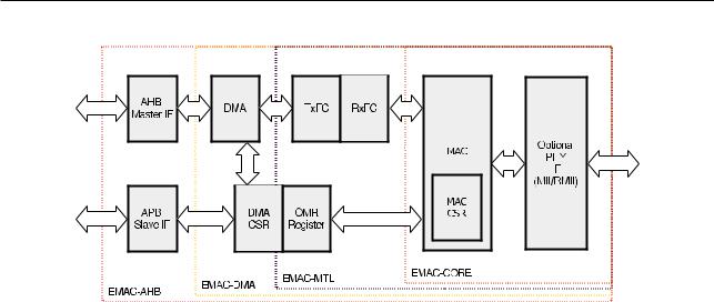
10 Ethernet Media Access Controller (MAC)
Figure 102. Ethernet Block Diagram
has two directions: Tx and Rx. They are connected to the system through the Advanced High-Performance Bus (AHB) and the Advanced Peripheral Bus (APB) on the chip. Off the chip, they communicate with the external PHY through the MII and RMII interfaces to establish an Ethernet connection.
10.2EMAC_CORE
The MAC supports many interfaces with the PHY chip. The PHY interface can be selected only once after reset. The MAC communicates with the application side (DMA side), using the MAC Transmit Interface (MTI), MAC Receive Interface (MRI) and the MAC Control Interface (MCI).
10.2.1 Transmit Operation
A transmit operation is initiated when the MTL Application pushes in data at the time a response signal is asserted. When the SOF (start of frame) signal is detected, the MAC accepts the data and begins transmitting to the RMII or MII. The time required to transmit the frame data to the RMII or MII, after the application initiates transmission, varies, depending on delay factors like IFG delay, time to transmit Preamble or SFD (Start Frame Delimiter), and any back-off delays in half-duplex mode. Until then, the MAC does not accept the data received from MTL by de-asserting the ready signal.
After the EOF (end of frame) is transmitted to the MAC, the MAC completes the normal transmission and yields the Transmit Status to the MTL. If a normal collision (in half-duplex mode) occurs during transmission, the MAC makes valid the Transmit Status in the MTL. It then accepts and drops all further data until the next SOF is received. The MTL block should retransmit the same frame from SOF upon observing a retry request (in the Status) from the MAC.
The MAC issues an underflow status if the MTL is not able to provide the data continuously during transmission. During the normal transmission of a frame from MTL, if the MAC receives an SOF without getting an EOF for the previous frame, it ignores the SOF and considers the new frame as a continuation of the previous one.
10.2.1.1 Transmit Flow Control
In full-duplex mode, when the Transmit Flow Control Enable bit (TFE bit in the Flow Control Register) is set to 1, the MAC will generate and send a pause frame, as needed. The pause frame is added and transmitted together with the calculated CRC. The generation of pause frames can be initiated in two ways.
Espressif Systems |
223 |
ESP32 TRM (Version 5.0) |
Submit Documentation Feedback

10 Ethernet Media Access Controller (MAC)
When the application sets the Flow Control Busy bit (FCB bit in the Flow Control Register) to 1, or when the Rx FIFO is full, a pause frame is transmitted.
•If an application has requested flow control by setting the FCB bit in the Flow Control Register to 1, the MAC will generate and send a single pause frame. The pause time value in the generated frame is the pause time value programmed in the Flow Control Register. To extend or end the pause time before the time specified in the previously transmitted pause frame, the application program must configure the pause time value in the Flow Control Register to the appropriate value and, then, request another pause frame transmission.
•If the application has requested flow control when the Rx FIFO is full, the MAC will generate and transmit a pause frame. The value of the pause time of the generated frame is the pause time value programmed in the Flow Control Register. If the Rx FIFO remains full during the configurable interval, which is determined by the Pause Low Threshold bit (PLT) in the Flow Control Register before the pause time expires, a second pause frame will be transmitted. As long as the Rx FIFO remains full, the process repeats itself. If the FIFO is no longer full before the sample time, the MAC will send a pause frame with zero pause time, indicating to the remote end that the Rx buffer is ready to receive the new data frame.
10.2.1.2 Retransmission During a Collision
In half-duplex mode, a collision may occur on the MAC line interface when frames are transmitted to the MAC. The MAC may even give a status to indicate a retry before the end of the frame is received. The retransmission is then enabled and the frame is popped out from the FIFO. When more than 96 bytes are transmitted to the MAC core, the FIFO controller frees the space in the FIFO, allowing the DMA to push more data into FIFO. This means that data cannot be retransmitted after the threshold is exceeded or when the MAC core indicates that a late collision has occurred.
The MAC transmitter may abort the transmission of a frame because of collision, Tx FIFO underflow, loss of carrier, jabber timeout, no carrier, excessive deferral, and late collision. When frame transmission is aborted because of collision, the MAC requests retransmission of the frame.
10.2.2 Receive Operation
A receive operation is initiated when the MAC detects an SFD on the RMII or MII. The MAC strips the Preamble and SFD before processing the frame. The header fields are checked for the filtering and the FCS (Frame Check Sequence) field used to verify the CRC for the frame. The received frame is stored in a shallow buffer until the address filtering is performed. The frame is dropped in the MAC if it fails the address filtering.
The frame received by the MAC will be pushed into the Rx FIFO. Once the FIFO status exceeds the Receive Threshold, configured by the Receive Threshold Control (RTC) bit in the Operation Mode register, the DMA can initiate a preconfigured burst transmission to the AHB interface.
In the default pass-through mode, when the FIFO receives a complete packet or 64 bytes configured by the RTC bit in the Operation Mode Register, the data pops up and its availability is notified to the DMA. After the DMA initiates the transmission to the AHB interface, the data transmission continues from the FIFO until the complete packet is transmitted. Upon completing transmitting the EOF, the status word will pop up and be transmitted to the DMA controller.
In the Rx FIFO Store-and-Forward mode (configured through the RSF or Receive Store and Forward bit in the Operation Mode Register), only the valid frames are read and forwarded to the application. In the passthrough mode, error frames are not discarded because the error status is received at the end of the frame. The start of frame will have been read from the FIFO at that point.
Espressif Systems |
224 |
ESP32 TRM (Version 5.0) |
Submit Documentation Feedback

10 Ethernet Media Access Controller (MAC)
10.2.2.1 Reception Protocol
After the receive module receives the packets, the Preamble and SFD of the received frames are removed. When the SFD is detected, the MAC starts sending Ethernet frame data to the Rx FIFO, starting at the first byte (destination address) following the SFD.
If the received frame length/type is less than 0x600 and the automatic CRC/Pad removal option is programmed for the MAC, the MAC will send frame data to the Rx FIFO (the amount of data does not exceed the number specified in the length/type field). Then MAC begins discarding the remaining section, including the FCS field. If the frame length/type is greater than, or equal to, 0x600, the MAC will send all received Ethernet frame data to the Rx FIFO, regardless of the programmed value of the automatic CRC removal option. By default, the MAC watchdog timer is enabled, meaning that frames, including DA, SA, LT, data, pad and FCS, which exceed 2048 bytes, are cut off. This function can be disabled by programming the Watchdog Disable (WD) bit in the MAC Configuration Register. However, even if the watchdog timer is disabled, frames longer than 16 KB will be cut off and the watchdog timeout status will be given.
10.2.2.2 Receive Frame Controller
If the RA (Receive All) bit in the MAC Frame Filter Register is reset, the MAC will filter frames based on the destination and source addresses. If the application decides not to receive any bad frames, such as runt frames and CRC error frames, another level of filtering is needed. When a frame fails the filtering, the frame is discarded and is not transmitted to the application. When the filter parameters are changed dynamically, if a frame fails the DA and SA filterings, the remaining part of the frame is discarded and the Receive Status word is updated immediately and, therefore, the zero frame length bit, CRC error bit, and runt frame error bit are set to 1. This indicates that the frame has failed the filtering.
10.2.2.3 Receive Flow Control
The MAC will detect the received pause frame and pause transmission of frames for a specified delay within the received pause frame (in full-duplex mode only). The Pause Frame Detect Function can be enabled or disabled by the RFCE (Receive Flow Control Enable) bit in the Flow Control Register. When receive flow control is enabled, it starts monitoring whether the destination address of the received frame matches the multicast address of the control frame (0x0180 C200 0001). If a match is detected (i.e. the destination address of the received frame matches the destination address of the reserved control frame), the MAC will determine whether to transmit the received control frame to the application, according to the PCF (Pass Control Frames) bit in the Frame Filter Register.
The MAC will also decode the type, the opcode, and the pause timer field of the Receive Control Frame. If the value of the status byte counter is 64 bits and there are no CRC errors, the MAC transmitter will halt the transmission of any data frame. The duration of the pause is the decoded pause time value multiplied by the interval (which is 64 bytes for both 10 Mbit/s and 100 Mb/s modes). At the same time, if another pause frame of zero pause time is detected, the MAC will reset the pause time to manage the new pause request.
If the type field (0x8808), the opcode (0x00001), and the byte length (64 bytes) of the received control frame are not 0x8808, 0x00001, and 64 bytes, respectively, or if there is a CRC error, the MAC will not generate a pause.
If a pause frame has a multicast destination address, the MAC filters the frame, according to the address matching.
For pause frames with a unicast destination address, the MAC checks whether the DA matches the content of the
Espressif Systems |
225 |
ESP32 TRM (Version 5.0) |
Submit Documentation Feedback