


9SD/MMC Host Controller
•Only one CE-ATA device at a time can be selected for a command or data transfer. For example, when data are transferred from a CE-ATA device, a new command should not be sent to another CE-ATA device.
•If a CE-ATA device’s interrupts are enabled (nIEN=0), a new RW_BLK command should not be sent to the same device if the execution of a RW_BLK command is already in progress (the RW_BLK command used in this databook is the RW_MULTIPLE_BLOCK MMC command defined by the CE-ATA specifications). Only the CCSD can be sent while waiting for the CCS.
•If, however, a CE-ATA device’s interrupts are disabled (nIEN=1), a new command can be issued to the same device, allowing it to read status information.
•Open-ended transfers are not supported in CE-ATA devices.
•The send_auto_stop signal is not supported (software should not set the send_auto_stop bit) in CE-ATA transfers.
After configuring the command start bit to 1, the values of the following registers cannot be changed before a command has been issued:
•CMD - command
•CMDARG - command argument
•BYTCNT - byte count
•BLKSIZ - block size
•CLKDIV - clock divider
•CKLENA - clock enable
•CLKSRC - clock source
•TMOUT - timeout
•CTYPE - card type
9.6RAM for Receiving and Sending Data
The submodule RAM is a buffer area for sending and receiving data. It can be divided into two units: the one is for sending data, and the other is for receiving data. The process of sending and receiving data can also be achieved by the CPU and DMA for reading and writing. The latter method is described in detail in Section 9.8.
9.6.1Transmit RAM Module
There are two ways to enable a write operation: DMA and CPU read/write.
If SDIO-sending is enabled, data can be written to the transferred RAM module by APB interface or DMA. Data will be written from register EMAC_FIFO to the CPU, directly, by an APB interface.
9.6.2Receive RAM Module
There are two ways to enable a read operation: DMA and CPU read/write.
When a subunit of the data path receives data, the subdata will be written onto the receive-RAM. Then, these subdata can be read either with the APB or the DMA method at the reading end. Register EMAC_FIFO can be read by the APB directly.
Espressif Systems |
196 |
ESP32 TRM (Version 5.0) |
Submit Documentation Feedback
9 SD/MMC Host Controller
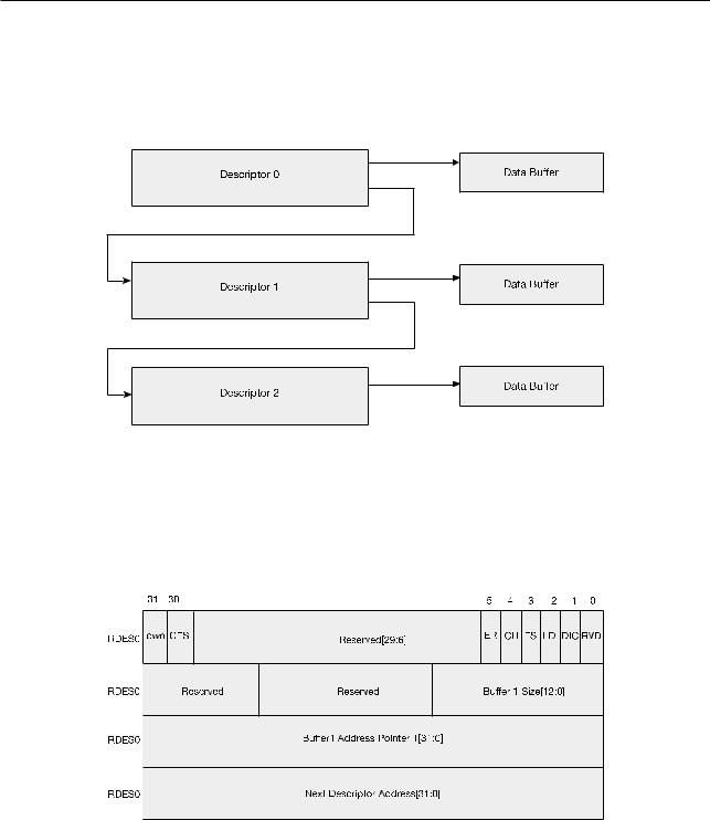
9.7Descriptor Chain
Each linked list module consists of two parts: the linked list itself and a data buffer. In other words, each module points to a unique data buffer and the linked list that follows the module. Figure 9-7 shows the descriptor chain.
Figure 97. Descriptor Chain
9.8The Structure of a Linked List
Each linked list consists of four words. As is shown below, Figure 9-8 demonstrates the linked list’s structure, and Table 9-2, Table 9-3, Table 9-4, Table 9-5 provide the descriptions of linked lists.
Figure 98. The Structure of a Linked List
The DES0 element contains control and status information.
|
|
|
Table 92. DES0 |
|
|
|
|
|
|
|
|
|
|
|
Bits |
Name |
|
Description |
|
|
|
|
|
|
When set, this bit indicates that the descriptor is |
|
|
|
31 |
OWN |
|
owned by the DMAC. When reset, it indicates that the |
|
|
|
|
descriptor is owned by the Host. The DMAC clears |
|
|||
|
|
|
|
|
||
|
|
|
|
this bit when it completes the data transfer. |
|
|
|
|
|
|
|
|
|
Espressif Systems |
|
197 |
ESP32 TRM (Version 5.0) |
|||
Submit Documentation Feedback

9 SD/MMC Host Controller
Bits |
Name |
Description |
|
|
|
These error bits indicate the status of the transition to |
|
|
|
or from the card. |
|
|
|
The following bits are also present in RINTSTS, which |
|
|
|
indicates their digital logic OR gate. |
|
|
|
• EBE: End Bit Error |
|
30 |
CES (Card Error Summary) |
• RTO: Response Time out |
|
|
|
• RCRC: Response CRC |
|
|
|
• SBE: Start Bit Error |
|
|
|
• DRTO: Data Read Timeout |
|
|
|
• DCRC: Data CRC for Receive |
|
|
|
• RE: Response Error |
|
|
|
|
|
29:6 |
Reserved |
Reserved |
|
|
|
|
|
|
|
When set, this bit indicates that the descriptor list has |
|
5 |
ER (End of Ring) |
reached its final descriptor. The DMAC then returns |
|
to the base address of the list, creating a Descriptor |
|||
|
|
||
|
|
Ring. |
|
|
|
|
|
|
CH |
When set, this bit indicates that the second address in |
|
4 |
the descriptor is the Next Descriptor address. When |
||
(Second Address Chained) |
|||
|
this bit is set, BS2 (DES1[25:13]) should be all zeros. |
||
|
|
||
|
|
|
|
|
|
When set, this bit indicates that this descriptor con- |
|
3 |
FD (First Descriptor) |
tains the first buffer of the data. If the size of the first |
|
buffer is 0, the Next Descriptor contains the beginning |
|||
|
|
||
|
|
of the data. |
|
|
|
|
|
|
|
This bit is associated with the last block of a DMA |
|
|
|
transfer. When set, the bit indicates that the buffers |
|
|
|
pointed by this descriptor are the last buffers of the |
|
2 |
LD (Last Descriptor) |
data. After this descriptor is completed, the remain- |
|
|
|
ing byte count is 0. In other words, after the descriptor |
|
|
|
with the LD bit set is completed, the remaining byte |
|
|
|
count should be 0. |
|
|
|
|
|
|
DIC (Disable Interrupt |
When set, this bit will prevent the setting of the TI/RI |
|
1 |
bit of the DMAC Status Register (IDSTS) for the data |
||
on Completion) |
|||
|
that ends in the buffer pointed by this descriptor. |
||
|
|
||
|
|
|
|
0 |
Reserved |
Reserved |
|
|
|
|
The DES1 element contains the buffer size.
|
|
Table 93. DES1 |
|
|
|
|
|
Bits |
Name |
|
Description |
31:26 |
Reserved |
|
Reserved |
|
|
|
|
25:13 |
Reserved |
|
Reserved |
|
|
|
|
Espressif Systems |
198 |
ESP32 TRM (Version 5.0) |
Submit Documentation Feedback