
- •1 System and Memory
- •1.1 Introduction
- •1.2 Features
- •1.3 Functional Description
- •1.3.1 Address Mapping
- •1.3.2 Embedded Memory
- •1.3.3 External Memory
- •1.3.5 Peripherals
- •2 Interrupt Matrix (INTERRUPT)
- •2.1 Overview
- •2.2 Features
- •2.3 Functional Description
- •2.3.1 Peripheral Interrupt Source
- •2.3.2 CPU Interrupt
- •2.3.3 Allocate Peripheral Interrupt Sources to Peripheral Interrupt on CPU
- •2.3.4 CPU NMI Interrupt Mask
- •2.3.5 Query Current Interrupt Status of Peripheral Interrupt Source
- •2.4 Registers
- •3 Reset and Clock
- •3.1 System Reset
- •3.1.1 Introduction
- •3.1.2 Reset Source
- •3.2 System Clock
- •3.2.1 Introduction
- •3.2.3 CPU Clock
- •3.2.4 Peripheral Clock
- •3.2.7 Audio PLL
- •3.3 Register Summary
- •3.4 Registers
- •4.1 Overview
- •4.2 Peripheral Input via GPIO Matrix
- •4.2.1 Summary
- •4.2.2 Functional Description
- •4.2.3 Simple GPIO Input
- •4.3 Peripheral Output via GPIO Matrix
- •4.3.1 Summary
- •4.3.3 Simple GPIO Output
- •4.4 Direct I/O via IO_MUX
- •4.4.1 Summary
- •4.4.2 Functional Description
- •4.5 RTC IO_MUX for Low Power and Analog I/O
- •4.5.1 Summary
- •4.5.2 Analog Function Description
- •4.7 Pad Hold Feature
- •4.8 I/O Pad Power Supplies
- •4.8.1 VDD_SDIO Power Domain
- •4.9 Peripheral Signal List
- •4.10 IO_MUX Pad List
- •4.11 RTC_MUX Pin List
- •4.12 Register Summary
- •4.12.1 GPIO Matrix Register Summary
- •4.12.2 IO MUX Register Summary
- •4.12.3 RTC IO MUX Register Summary
- •4.13 Registers
- •4.13.1 GPIO Matrix Registers
- •4.13.2 IO MUX Registers
- •4.13.3 RTC IO MUX Registers
- •5 DPort Registers
- •5.1 Introduction
- •5.2 Features
- •5.3 Functional Description
- •5.3.1 System and Memory Register
- •5.3.2 Reset and Clock Registers
- •5.3.3 Interrupt Matrix Register
- •5.3.4 DMA Registers
- •5.3.5 MPU/MMU Registers
- •5.3.7 Peripheral Clock Gating and Reset
- •5.4 Register Summary
- •5.5 Registers
- •6 DMA Controller (DMA)
- •6.1 Overview
- •6.2 Features
- •6.3 Functional Description
- •6.3.1 DMA Engine Architecture
- •6.3.2 Linked List
- •6.4 UART DMA (UDMA)
- •7 SPI Controller (SPI)
- •7.1 Overview
- •7.5 Parallel QSPI
- •7.5.1 Communication Format of Parallel QSPI
- •7.6.1 SPI Interrupts
- •7.6.2 DMA Interrupts
- •7.7 Register Summary
- •7.8 Registers
- •8 SDIO Slave Controller
- •8.1 Overview
- •8.2 Features
- •8.3 Functional Description
- •8.3.1 SDIO Slave Block Diagram
- •8.3.3 Register Access
- •8.3.6 SDIO Bus Timing
- •8.3.7 Interrupt
- •8.4 Register Summary
- •8.5 SLC Registers
- •8.6 SLC Host Registers
- •8.7 HINF Registers
- •9 SD/MMC Host Controller
- •9.1 Overview
- •9.2 Features
- •9.3 SD/MMC External Interface Signals
- •9.4 Functional Description
- •9.4.1 SD/MMC Host Controller Architecture
- •9.4.2 Command Path
- •9.4.3 Data Path
- •9.5 Software Restrictions for Proper CIU Operation
- •9.6 RAM for Receiving and Sending Data
- •9.6.1 Transmit RAM Module
- •9.6.2 Receive RAM Module
- •9.8 The Structure of a Linked List
- •9.9 Initialization
- •9.9.1 DMAC Initialization
- •9.9.2 DMAC Transmission Initialization
- •9.9.3 DMAC Reception Initialization
- •9.11 Interrupt
- •9.12 Register Summary
- •9.13 Registers
- •10 Ethernet Media Access Controller (MAC)
- •10.1 Overview
- •10.2 EMAC_CORE
- •10.2.1 Transmit Operation
- •10.2.2 Receive Operation
- •10.3 MAC Interrupt Controller
- •10.4 MAC Address Filtering
- •10.4.1 Unicast Destination Address Filtering
- •10.4.2 Multicast Destination Address Filtering
- •10.4.3 Broadcast Address Filtering
- •10.4.4 Unicast Source Address Filtering
- •10.4.5 Inverse Filtering Operation
- •10.4.6 Good Transmitted Frames and Received Frames
- •10.5 EMAC_MTL (MAC Transaction Layer)
- •10.6 PHY Interface
- •10.6.1 MII (Media Independent Interface)
- •10.6.3 Station Management Agent (SMA) Interface
- •10.6.4 RMII Timing
- •10.7 Ethernet DMA Features
- •10.8 Linked List Descriptors
- •10.8.1 Transmit Descriptors
- •10.8.2 Receive Descriptors
- •10.9 Register Summary
- •10.10 Registers
- •11 I2C Controller (I2C)
- •11.1 Overview
- •11.2 Features
- •11.3 Functional Description
- •11.3.1 Introduction
- •11.3.2 Architecture
- •11.3.3 I2C Bus Timing
- •11.3.7 Interrupts
- •11.4 Register Summary
- •11.5 Registers
- •12 I2S Controller (I2S)
- •12.1 Overview
- •12.2 Features
- •12.3 The Clock of I2S Module
- •12.4 I2S Mode
- •12.4.1 Supported Audio Standards
- •12.4.2 Module Reset
- •12.4.3 FIFO Operation
- •12.4.5 Receiving Data
- •12.5.1 LCD Master Transmitting Mode
- •12.5.2 Camera Slave Receiving Mode
- •12.5.3 ADC/DAC mode
- •12.6 I2S Interrupts
- •12.6.1 FIFO Interrupts
- •12.6.2 DMA Interrupts
- •12.7 Register Summary
- •12.8 Registers
- •13 UART Controller (UART)
- •13.1 Overview
- •13.2 UART Features
- •13.3 Functional Description
- •13.3.1 Introduction
- •13.3.3 UART RAM
- •13.3.5 UART Data Frame
- •13.3.7 Flow Control
- •13.3.8 UART DMA
- •13.3.9 UART Interrupts
- •13.3.10 UHCI Interrupts
- •13.4 Register Summary
- •13.4.1 UART Register Summary
- •13.5 Registers
- •13.5.1 UART Registers
- •13.5.2 UHCI Registers
- •14 LED PWM Controller (LEDC)
- •14.1 Introduction
- •14.2 Functional Description
- •14.2.1 Architecture
- •14.2.3 Channels
- •14.2.4 Interrupts
- •14.3 Register Summary
- •14.4 Registers
- •15 Remote Control Peripheral (RMT)
- •15.1 Introduction
- •15.2 Functional Description
- •15.2.1 RMT Architecture
- •15.2.3 Clock
- •15.2.4 Transmitter
- •15.2.5 Receiver
- •15.2.6 Interrupts
- •15.3 Register Summary
- •15.4 Registers
- •16 Motor Control PWM (PWM)
- •16.1 Introduction
- •16.2 Features
- •16.3 Submodules
- •16.3.1 Overview
- •16.3.2 PWM Timer Submodule
- •16.3.3 PWM Operator Submodule
- •16.3.4 Capture Submodule
- •16.4 Register Summary
- •16.5 Registers
- •17 Pulse Count Controller (PCNT)
- •17.1 Overview
- •17.2 Functional Description
- •17.2.1 Architecture
- •17.2.2 Counter Channel Inputs
- •17.2.3 Watchpoints
- •17.2.4 Examples
- •17.2.5 Interrupts
- •18 Timer Group (TIMG)
- •18.1 Introduction
- •18.2 Functional Description
- •18.2.2 64-bit Time-base Counter
- •18.2.3 Alarm Generation
- •18.2.4 MWDT
- •18.2.5 Interrupts
- •18.3 Register Summary
- •18.4 Registers
- •19 Watchdog Timers (WDT)
- •19.1 Introduction
- •19.2 Features
- •19.3 Functional Description
- •19.3.1 Clock
- •20 eFuse Controller
- •20.1 Introduction
- •20.2 Features
- •20.3 Functional Description
- •20.3.1 Structure
- •20.3.3 Software Reading of System Parameters
- •20.3.4 The Use of System Parameters by Hardware Modules
- •20.3.5 Interrupts
- •20.4 Register Summary
- •20.5 Registers
- •21 Two-wire Automotive Interface (TWAI)
- •21.1 Overview
- •21.2 Features
- •21.3 Functional Protocol
- •21.3.1 TWAI Properties
- •21.3.2 TWAI Messages
- •21.3.3 TWAI Errors
- •21.3.4 TWAI Bit Timing
- •21.4 Architectural Overview
- •21.4.1 Registers Block
- •21.4.2 Bit Stream Processor
- •21.4.3 Error Management Logic
- •21.4.4 Bit Timing Logic
- •21.4.5 Acceptance Filter
- •21.5 Functional Description
- •21.5.1 Modes
- •21.5.2 Bit Timing
- •21.5.3 Interrupt Management
- •21.5.4 Transmit and Receive Buffers
- •21.5.5 Receive FIFO and Data Overruns
- •21.5.6 Acceptance Filter
- •21.5.8 Error Code Capture
- •21.5.9 Arbitration Lost Capture
- •21.6 Register Summary
- •21.7 Registers
- •22 AES Accelerator (AES)
- •22.1 Introduction
- •22.2 Features
- •22.3 Functional Description
- •22.3.1 AES Algorithm Operations
- •22.3.2 Key, Plaintext and Ciphertext
- •22.3.3 Endianness
- •22.3.4 Encryption and Decryption Operations
- •22.3.5 Speed
- •22.4 Register Summary
- •22.5 Registers
- •23 SHA Accelerator (SHA)
- •23.1 Introduction
- •23.2 Features
- •23.3 Functional Description
- •23.3.1 Padding and Parsing the Message
- •23.3.2 Message Digest
- •23.3.3 Hash Operation
- •23.3.4 Speed
- •23.4 Register Summary
- •23.5 Registers
- •24 RSA Accelerator (RSA)
- •24.1 Introduction
- •24.2 Features
- •24.3 Functional Description
- •24.3.1 Initialization
- •24.3.2 Large Number Modular Exponentiation
- •24.3.4 Large Number Multiplication
- •24.4 Register Summary
- •24.5 Registers
- •25 Random Number Generator (RNG)
- •25.1 Introduction
- •25.2 Feature
- •25.3 Functional Description
- •25.5 Register Summary
- •25.6 Register
- •26 External Memory Encryption and Decryption (FLASH)
- •26.1 Overview
- •26.2 Features
- •26.3 Functional Description
- •26.3.1 Key Generator
- •26.3.2 Flash Encryption Block
- •26.3.3 Flash Decryption Block
- •26.4 Register Summary
- •26.5 Register
- •27 Memory Management and Protection Units (MMU, MPU)
- •27.1 Introduction
- •27.2 Features
- •27.3 Functional Description
- •27.3.1 PID Controller
- •28 Process ID Controller (PID)
- •28.1 Overview
- •28.2 Features
- •28.3 Functional Description
- •28.3.1 Interrupt Identification
- •28.3.2 Information Recording
- •28.3.3 Proactive Process Switching
- •28.4 Register Summary
- •28.5 Registers
- •29 On-Chip Sensors and Analog Signal Processing
- •29.1 Introduction
- •29.2 Capacitive Touch Sensor
- •29.2.1 Introduction
- •29.2.2 Features
- •29.2.3 Available GPIOs
- •29.2.4 Functional Description
- •29.2.5 Touch FSM
- •29.3.1 Introduction
- •29.3.2 Features
- •29.3.3 Outline of Function
- •29.3.4 RTC SAR ADC Controllers
- •29.3.5 DIG SAR ADC Controllers
- •29.4.1 Introduction
- •29.4.2 Features
- •29.4.4 Cosine Waveform Generator
- •29.5 Register Summary
- •29.5.1 Sensors
- •29.5.2 Advanced Peripheral Bus
- •29.6 Registers
- •29.6.1 Sensors
- •29.6.2 Advanced Peripheral Bus
- •30 ULP Coprocessor (ULP)
- •30.1 Introduction
- •30.2 Features
- •30.4 Instruction Set
- •30.4.2 ST – Store Data in Memory
- •30.4.3 LD – Load Data from Memory
- •30.4.4 JUMP – Jump to an Absolute Address
- •30.4.5 JUMPR – Jump to a Relative Offset (Conditional upon R0)
- •30.4.7 HALT – End the Program
- •30.4.8 WAKE – Wake up the Chip
- •30.4.10 WAIT – Wait for a Number of Cycles
- •30.4.12 I2C_RD/I2C_WR – Read/Write I²C
- •30.4.13 REG_RD – Read from Peripheral Register
- •30.5 ULP Program Execution
- •30.6 RTC_I2C Controller
- •30.6.1 Configuring RTC_I2C
- •30.6.2 Using RTC_I2C
- •30.7 Register Summary
- •30.7.1 SENS_ULP Address Space
- •30.7.2 RTC_I2C Address Space
- •30.8 Registers
- •30.8.1 SENS_ULP Address Space
- •30.8.2 RTC_I2C Address Space
- •31 Low-Power Management (RTC_CNTL)
- •31.1 Introduction
- •31.2 Features
- •31.3 Functional Description
- •31.3.2 Digital Core Voltage Regulator
- •31.3.4 Flash Voltage Regulator
- •31.3.5 Brownout Detector
- •31.3.6 RTC Module
- •31.3.9 Predefined Power Modes
- •31.3.10 Wakeup Source
- •31.3.12 RTC Timer
- •31.3.13 RTC Boot
- •31.4 Register Summary
- •31.5 Registers
- •Glossary
- •Abbreviations for Peripherals
- •Abbreviations for Registers
- •Revision History

8SDIO Slave Controller
8.1Overview
The ESP32 features hardware support for the industry-standard Secure Digital (SD) device interface that conforms to the SD Input/Output (SDIO) Specification Version 2.0. This allows a host controller to access the ESP32 via an SDIO bus protocol, enabling high-speed data transfer.
The SDIO interface may be used to read ESP32 SDIO registers directly and access shared memory via Direct Memory Access (DMA), thus reducing processing overhead while maintaining high performance.
8.2Features
•Meets SDIO V2.0 specification
•Supports SDIO SPI, 1-bit, and 4-bit transfer modes
•Full host clock range of 0 ~ 50 MHz
•Configurable sample and drive clock edge
•Integrated, SDIO-accessible registers for information interaction
•Supports SDIO interrupt mechanism
•Automatic data padding
•Block size of up to 512 bytes
•Interrupt vector between Host and Slave for bidirectional interrupt
•Supports DMA for data transfer
8.3Functional Description
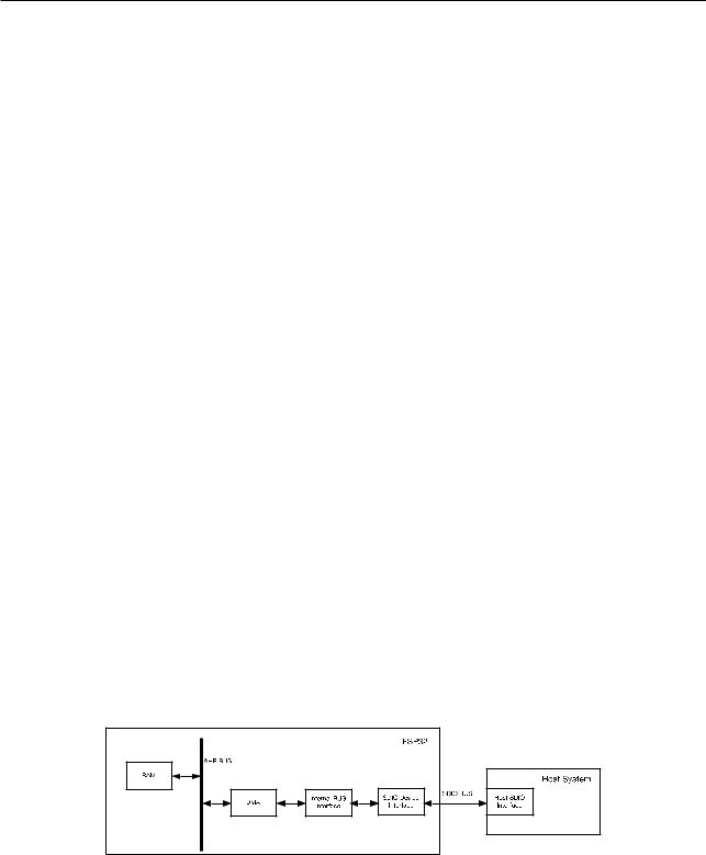
8.3.1SDIO Slave Block Diagram
The functional block diagram of the SDIO slave module is shown in Figure 8-1.
Figure 81. SDIO Slave Block Diagram
The Host System represents any SDIO specification V2.0-compatible host device. The Host System interacts with the ESP32 (configured as the SDIO slave) via the standard SDIO bus implementation.
The SDIO Device Interface block enables effective communication with the external Host by directly providing SDIO interface registers and enabling DMA operation for high-speed data transfer over the Advanced High-performance Bus (AHB) without engaging the CPU.
Espressif Systems |
159 |
ESP32 TRM (Version 5.0) |
Submit Documentation Feedback

8 SDIO Slave Controller
8.3.2Sending and Receiving Data on SDIO Bus
Data is transmitted between Host and Slave through the SDIO bus I/O Function1. After the Host enables the I/O Function1 in the Slave, according to the SDIO protocol, data transmission will begin.
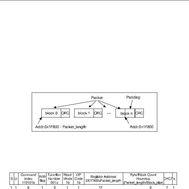
ESP32 segregates data into packets sent to/from the Host. To achieve high bus utilization and data transfer rates, we recommend the single block transmission mode. For detailed information on this mode, please refer to the SDIO V2.0 protocol specification. When Host and Slave exchange data as blocks on the SDIO bus, the Slave automatically pads data-when sending data out-and automatically strips padding data from the incoming data block.
Whether the Slave pads or discards the data depends on the data address on the SDIO bus. When the data address is equal to, or greater than, 0x1F800, the Slave will start padding or discarding data. Therefore, the starting data address should be 0x1F800 - Packet_length, where Packet_length is measured in bytes. Data flow on the SDIO bus is shown in Figure 8-2.
Figure 82. SDIO Bus Packet Transmission
The standard IO_RW_EXTENDED (CMD53) command is used to initiate a packet transfer of an arbitrary length. The content of the CMD53 command used in data transmission is as illustrated in Figure 8-3 below. For detailed information on CMD53, please refer to the SDIO protocol specifications.
Figure 83. CMD53 Content
8.3.3Register Access
For effective interaction between Host and Slave, the Host can access certain registers in the Slave via the SDIO bus I/O Function1. These registers are in continuous address fields from SLC0HOST_TOKEN_RDATA to SLCHOST_INF_ST. The Host device can access these registers by simply setting the register addresses of CMD52 or CMD53 to the low 10 bits of the corresponding register address. The Host can access several consecutive registers at one go with CMD53, thus achieving a higher effective transfer rate.
There are 54 bytes of field between SLCHOST_CONF_W0_REG and SLCHOST_CONF_W15_REG. Host and Slave can access and change these fields, thus facilitating the information interaction between Host and Slave.
8.3.4DMA
The SDIO Slave module uses dedicated DMA to access data residing in the RAM. As shown in Figure 8-1, the RAM is accessed over the AHB. DMA accesses RAM through a linked-list descriptor. Every linked list is
Espressif Systems |
160 |
ESP32 TRM (Version 5.0) |
Submit Documentation Feedback

8 SDIO Slave Controller
composed of three words, as shown in Figure 8-4.
Figure 84. SDIO Slave DMA Linked List Structure
•Owner: The allowed operator of the buffer that corresponds to the current linked list. 0: CPU is the allowed operator; 1: DMA is the allowed operator.
•Eof: End-of-file marker, indicating that this linked-list element is the last element of the data packet.
•Length: The number of valid bytes in the buffer, i.e., the number of bytes that should be accessed from the buffer for reading/writing.
•Size: The maximum number of available buffers.
•Buffer Address Pointer: The address of the data buffer as seen by the CPU (according to the RAM address space).
•Next Descriptor Address: The address of the next linked-list element in the CPU RAM address space. If the current linked list is the last one, the Eof bit should be 1, and the last descriptor address should be 0.
The Slave’s linked-list chain is shown in Figure 8-5:
Figure 85. SDIO Slave Linked List
8.3.5PacketSending/Receiving Procedure
The SDIO Host and Slave devices need to follow specific data transfer procedures to successfully exchange data over the SDIO interface.
Espressif Systems |
161 |
ESP32 TRM (Version 5.0) |
Submit Documentation Feedback

8 SDIO Slave Controller
8.3.5.1Sending Packets to SDIO Host
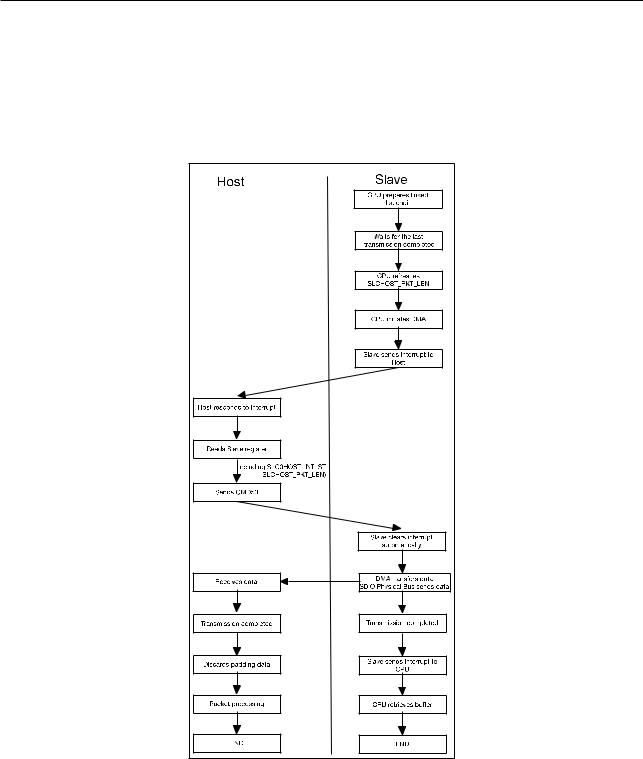
The transmission of packets from Slave to Host is initiated by the Slave. The Host will be notified with an interrupt (for detailed information on interrupts, please refer to SDIO protocol). After the Host reads the relevant information from the Slave, it will initiate an SDIO bus transaction accordingly. The whole procedure is illustrated in Figure 8-6.
Figure 86. Packet Sending Procedure (Initiated by Slave)
When the Host is interrupted, it reads relevant information from the Slave by visiting registers SLC0HOST_INT and SLCHOST_PKT_LEN.
•SLC0HOST_INT: Interrupt status register. If the value of SLC0_RX_NEW_PACKET_INT_ST is 1, this indicates that the Slave has a packet to send.
•SLCHOST_PKT_LEN: Packet length accumulator register. The current value minus the value of last time equals the packet length sent this time.
In order to start DMA, the CPU needs to write the low 20 bits of the address of the first linked-list element to the
Espressif Systems |
162 |
ESP32 TRM (Version 5.0) |
Submit Documentation Feedback

8 SDIO Slave Controller
SLC0_RXLINK_ADDR bit of SLC0RX_LINK, then set the SLC0_RXLINK_START bit of SLC0RX_LINK. The DMA will automatically complete the data transfer. Upon completion of the operation, DMA will interrupt the CPU so that the buffer space can be freed or reused.
8.3.5.2Receiving Packets from SDIO Host
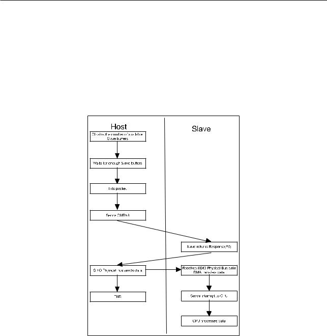
Transmission of packets from Host to Slave is initiated by the Host. The Slave receives data via DMA and stores it in RAM. After transmission is completed, the CPU will be interrupted to process the data. The whole procedure is demonstrated in Figure 8-7.
Figure 87. Packet Receiving Procedure (Initiated by Host)
The Host obtains the number of available receiving buffers from the Slave by accessing register SLC0HOST_TOKEN_RDATA. The Slave CPU should update this value after the receiving DMA linked list is prepared.
HOSTREG_SLC0_TOKEN1 in SLC0HOST_TOKEN_RDATA stores the accumulated number of available buffers.
The Host can figure out the available buffer space, using HOSTREG_SLC0_TOKEN1 minus the number of buffers already used.
If the buffers are not enough, the Host needs to constantly poll the register until there are enough buffers available.
To ensure sufficient receiving buffers, the Slave CPU must constantly load buffers on the receiving linked list. The process is shown in Figure 8-8.
Espressif Systems |
163 |
ESP32 TRM (Version 5.0) |
Submit Documentation Feedback