

7SPI Controller (SPI)
7SPI Controller (SPI)
7.1 |
Overview |
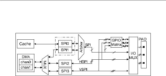
Figure 71. SPI Architecture
As Figure 7-1 shows, ESP32 integrates four SPI controllers which can be used to communicate with external devices that use the SPI protocol. Controller SPI0 is used as a buffer for accessing external memory. Controller SPI1 can be used as a master. Controllers SPI2 and SPI3 can be configured as either a master or a slave. When used as a master, each SPI controller can drive multiple CS signals (CS0~CS2) to activate multiple slaves. Controllers SPI1~SPI3 share two DMA channels.
The SPI signal buses consist of D, Q, CS0-CS2, CLK, WP, and HD signals, as Table 7-1 shows. Controllers SPI0 and SPI1 share one signal bus through an arbiter; the signals of the shared bus start with “SPI”. Controllers SPI2 and SPI3 use signal buses starting with “HSPI” and “VSPI” respectively. The I/O lines included in the abovementioned signal buses can be mapped to pins via either the IO_MUX module or the GPIO matrix. (Please refer to Chapter IO_MUX for details.)
The SPI controller supports four-line full-duplex/half-duplex communication (MOSI, MISO, CS, and CLK lines) and three-line half-duplex-only communication (DATA, CS, and CLK lines) in GP-SPI mode. In QSPI mode, an SPI controller accesses the flash or SRAM by using signal buses D, Q, CS0~CS2, CLK, WP, and HD as a four-bit parallel SPI bus. The mapping between SPI bus signals and pin function signals under different communication modes is shown in Table 7-1.
Table 71. Mapping Between SPI Bus Signals and Pin Function Signals
Four-line GP-SPI |
Three-line GP-SPI |
QSPI |
Pin function signals |
||
Full-duplex/half- |
Half-duplex signal |
Signal bus |
SPI signal |
HSPI signal |
VSPI signal |
duplex signal bus |
bus |
|
bus |
bus |
bus |
MOSI |
DATA |
D |
SPID |
HSPID |
VSPID |
|
|
|
|
|
|
MISO |
- |
Q |
SPIQ |
HSPIQ |
VSPIQ |
|
|
|
|
|
|
CS |
CS |
CS |
SPICS0 |
HSPICS0 |
VSPICS0 |
|
|
|
|
|
|
CLK |
CLK |
CLK |
SPICLK |
HSPICLK |
VSPICLK |
|
|
|
|
|
|
- |
- |
WP |
SPIWP |
HSPIWP |
VSPIWP |
|
|
|
|
|
|
- |
- |
HD |
SPIHD |
HSPIHD |
VSPIHD |
|
|
|
|
|
|
Espressif Systems |
125 |
ESP32 TRM (Version 5.0) |
Submit Documentation Feedback
7 SPI Controller (SPI)
7.2SPI Features
General Purpose SPI (GPSPI)
•Programmable data transfer length, in multiples of 1 byte
•Four-line full-duplex/half-duplex communication and three-line half-duplex communication support
•Master mode and slave mode
•Programmable CPOL and CPHA
•Programmable clock
Parallel QSPI
•Communication format support for specific slave devices such as flash
•Programmable communication format
•Six variations of flash-read operations available
•Automatic shift between flash and SRAM access
•Automatic wait states for flash access
SPI DMA Support
• Support for sending and receiving data using linked lists
SPI Interrupt Hardware
•SPI interrupts
•SPI DMA interrupts
7.3GPSPI
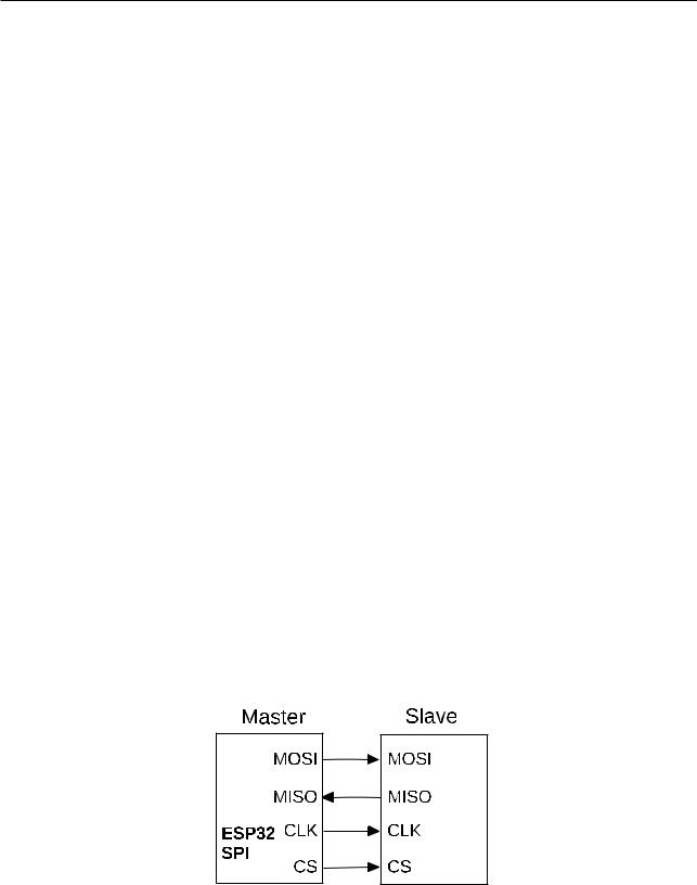
The SPI master mode supports four-line full-duplex/half-duplex communication and three-line half-duplex communication. Figure 7-2 outlines the connections needed for four-line full-duplex/half-duplex communications.
Figure 72. SPI Master and Slave Fullduplex/Halfduplex Communication
The SPI1~SPI3 controllers can communicate with other slaves as a standard SPI master. SPI2 and SPI3 can be configured as either a master or a slave. Every SPI master can be connected to three slaves at most by default. When not using DMA, the maximum length of data received/sent in one burst is 64 bytes. The data length is in multiples of one byte.
Espressif Systems |
126 |
ESP32 TRM (Version 5.0) |
Submit Documentation Feedback

7 SPI Controller (SPI)
Table 72. Command Definitions Supported by GPSPI Slave in Halfduplex Mode
Command |
Description |
|
0x1 |
Received by slave; writes data sent by the master into the slave status register via MOSI. |
|
|
|
|
0x2 |
Received by slave; writes data sent by the master into the slave data buffer via MOSI. |
|
|
|
|
0x3 |
Sent by slave; sends data in the slave buffer to master via MISO. |
|
|
|
|
0x4 |
Sent by slave; sends data in the slave status register to master via MISO. |
|
|
|
|
0x6 |
Writes master data on MOSI into data buffer and then sends the date in the slave data buffer |
|
to MISO. |
||
|
||
|
|
7.3.1GPSPI Fourline Fullduplex Communication
When configured to four-line full-duplex mode, the ESP32 SPI can act as either a master or a slave. The length of received and sent data needs to be set by configuring the SPI_MISO_DLEN_REG, SPI_MOSI_DLEN_REG registers for master mode as well as SPI_SLV_RDBUF_DLEN_REG, SPI_SLV_WRBUF_DLEN_REG registers for slave mode. The SPI_DOUTDIN bit and SPI_USR_MOSI bit in register SPI_USER_REG should be configured to enable this communication mode. The SPI_USR bit in register SPI_CMD_REG needs to be configured to initialize a data transfer.
7.3.2GPSPI Fourline Halfduplex Communication
When configured to four-line half-duplex mode, the ESP32 SPI can act as either a master or a slave. In this mode, the SPI communication supports flexible communication format as: command + address + dummy phase
+received and/or sent data. The format is specified as follows:
1.command: length of 0~16 bits; Master Out Slave In (MOSI).
2.address: length of 0~32/64 bits; Master Out Slave In (MOSI).
3.dummy phase: length of 0~256 SPI clocks.
4.received and/or sent data: length of 0~512 bits (64 bytes); Master Out Slave In (MOSI) or Master In Slave Out (MISO).
The address length is up to 32 bits in GP-SPI master mode and 64 bits in QSPI master mode. The command phase, address phase, dummy phase and received/sent data phase are controlled by bits SPI_USR_COMMAND, SPI_USR_ADDR, SPI_USR_DUMMY, and SPI_USR_MISO/SPI_USR_MOSI respectively in register SPI_USER_REG. A certain phase is enabled only when its corresponding control bit is set to 1. Details can be found in register description. When SPI works as a master, the register can be configured by software as required to determine whether or not to enable a certain phase.
When SPI works as a slave, the communication format must contain command, address, received and/or sent data, among which the command has several options listed in Table 7-2. During data transmission or reception, the CS signal should keep logic level low. If the CS signal is pulled up during transmission, the internal state of the slave will be reset.
The master can write the slave status register SPI_SLV_WR_STATUS_REG, and decide whether to read data from register SPI_SLV_WR_STATUS_REG or register SPI_RD_STATUS_REG via the SPI_SLV_STATUS_READBACK bit in register SPI_SLAVE1_REG. The SPI master can maintain communication with the slave by reading and writing slave status register, thus realizing complex communication with ease.
The length of received and sent data is controlled by SPI_MISO_DLEN_REG and SPI_MOSI_DLEN_REG in master mode, as well as SPI_SLV_RDBUF_DLEN_REG and SPI_SLV_WRBUF_DLEN_REG in slave mode. A reception or
Espressif Systems |
127 |
ESP32 TRM (Version 5.0) |
Submit Documentation Feedback
7 SPI Controller (SPI)
transmission of data is controlled by bit SPI_USR_MOSI or SPI_USR_MISO in SPI_USER_REG. The SPI_USR bit in register SPI_CMD_REG needs to be configured to initialize a data transfer.
7.3.3GPSPI Threeline Halfduplex Communication
The three-line half-duplex communication differs from four-line half-duplex communication in that the reception and transmission shares one signal bus and that the communication format must contain command, address, received and/or sent data. Software can enable three-line half-duplex communication by configuring SPI_SIO bit in SPI_USER_REG register.
Note:
•In half-duplex communication, the order of command, address, received and/or sent data in the communication format should be followed strictly.
•In half-duplex communication, communication formats ”command + address + received data + sent data” and ”received data + sent data” are not applicable to DMA.
•When ESP32 SPI acts as a slave, the master CS should be active at least one SPI clock period before a read/write process is initiated, and should be inactive at least one SPI clock period after the read/write process is completed.
7.3.4GPSPI Data Buffer
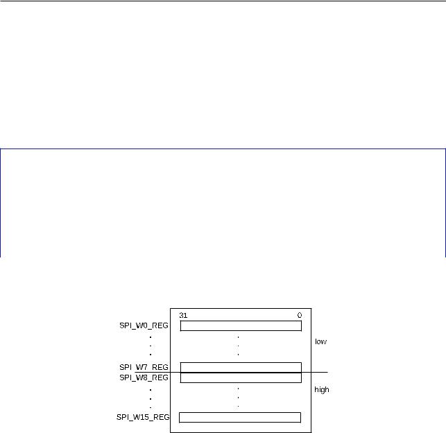
Figure 73. SPI Data Buffer
ESP32 SPI has 16 × 32 bits of data buffer to buffer data-send and data-receive operations. As is shown in Figure 7-3, received data is written from the low byte of SPI_W0_REG by default and the writing ends with SPI_W15_REG. If the data length is over 64 bytes, the extra part will be written from SPI_W0_REG.
Data buffer blocks SPI_W0_REG ~ SPI_W7_REG and SPI_W8_REG ~ SPI_W15_REG data correspond to the lower part and the higher part respectively. They can be used separately, and are controlled by the SPI_USR_MOSI _HIGHPART bit and the SPI_USR_MISO_HIGHPART bit in register SPI_USER_REG. For example, if SPI is configured as a master, when SPI_USR_MOSI_HIGHPART = 1, SPI_W8_REG ~ SPI_W15_REG are used as buffer for sending data; when SPI_USR_MISO_HIGHPART = 1, SPI_W8_REG ~ SPI_W15_REG are used as buffer for receiving data. If SPI acts as a slave, when SPI_USR_MOSI_HIGHPART = 1, SPI_W8_REG ~ SPI_W15_REG are used as buffer for receiving data; when SPI_USR_MISO_HIGHPART = 1, SPI_W8_REG ~ SPI_W15_REG are used as buffer for sending data.
Espressif Systems |
128 |
ESP32 TRM (Version 5.0) |
Submit Documentation Feedback

7 SPI Controller (SPI)
Table 73. Clock Polarity and Phase, and Corresponding SPI Register Values for SPI Master
Registers |
mode0 |
mode1 |
mode2 |
mode3 |
SPI_CK_IDLE_EDGE |
0 |
0 |
1 |
1 |
|
|
|
|
|
SPI_CK_OUT_EDGE |
0 |
1 |
1 |
0 |
|
|
|
|
|
SPI_MISO_DELAY_MODE |
2(0) |
1(0) |
1(0) |
2(0) |
|
|
|
|
|
SPI_MISO_DELAY_NUM |
0 |
0 |
0 |
0 |
|
|
|
|
|
SPI_MOSI_DELAY_MODE |
0 |
0 |
0 |
0 |
|
|
|
|
|
SPI_MOSI_DELAY_NUM |
0 |
0 |
0 |
0 |
|
|
|
|
|
7.4GPSPI Clock Control
The maximum output clock frequency of ESP32 GP-SPI master is fapb/2, and the maximum input clock frequency of the ESP32 GP-SPI slave is fapb/8. The master can derive other clock frequencies via frequency division.
fapb
fspi = (SPI_CLKCNT_N+1)(SPI_CLKDIV_PRE+1)
SPI_CLKCNT_N and SPI_CLKDIV_PRE are two bits of register SPI_CLOCK_REG (Please refer to 7.7 Regis-
ter Description for details). SPI_CLKCNT_H = SPI_CLKCNT_N+1 –1 , SPI_CLKCNT_N=SPI_CLKCNT_L. When the
2
SPI_CLK_EQU_SYSCLK bit in register SPI_CLOCK_REG is set to 1, and the other bits are set to 0, SPI output clock frequency is fapb. For other clock frequencies, SPI_CLK_EQU_SYSCLK needs to be 0. In slave mode, SPI_CLKCNT_N, SPI_CLKCNT_L, SPI_CLKCNT_H and SPI_CLKDIV_PRE should all be 0.
7.4.1GPSPI Clock Polarity (CPOL) and Clock Phase (CPHA)
The clock polarity and clock phase of ESP32 SPI are controlled by SPI_CK_IDLE_EDGE bit in register SPI_PIN_REG, SPI_CK_OUT_EDGE bit and SPI_CK_I_EDGE bit in register SPI_USER_REG, as well as SPI_MISO_DELAY_MODE[1:0] bit, SPI_MISO_DELAY_NUM[2:0] bit, SPI_MOSI_DELAY_MODE[1:0] bit, SPI_MOSI_DELAY_MUM[2:0] bit in register SPI_CTRL2_REG. Table 7-3 and Table 7-4 show the clock polarity and phase as well as the corresponding register values for ESP32 SPI master and slave, respectively. Note that for mode0 and mode2 in Table 7-4, the registers are configured differently in non-DMA mode and DMA mode, and that the SPI slave data is output in advance in DMA mode.
Table 74. Clock Polarity and Phase, and Corresponding SPI Register Values for SPI Slave
Registers |
mode0 |
mode1 |
mode2 |
mode3 |
|||
|
Non-DMA |
|
DMA |
|
Non-DMA |
DMA |
|
SPI_CK_IDLE_EDGE |
1 |
0 |
1 |
0 |
1 |
0 |
|
|
|
|
|
|
|
|
|
SPI_CK_I_EDGE |
0 |
1 |
1 |
1 |
0 |
0 |
|
|
|
|
|
|
|
|
|
SPI_MISO_DELAY_MODE |
0 |
0 |
2 |
0 |
0 |
1 |
|
|
|
|
|
|
|
|
|
SPI_MISO_DELAY_NUM |
0 |
2 |
0 |
0 |
2 |
0 |
|
|
|
|
|
|
|
|
|
SPI_MOSI_DELAY_MODE |
2 |
0 |
0 |
1 |
0 |
0 |
|
|
|
|
|
|
|
|
|
SPI_MOSI_DELAY_NUM |
2 |
3 |
0 |
2 |
3 |
0 |
|
|
|
|
|
|
|
|
|
1.mode0 means CPOL=0, CPHA=0. When SPI is idle, the clock output is logic low; data changes on the falling edge of the SPI clock and is sampled on the rising edge;
2.mode1 means CPOL=0, CPHA=1. When SPI is idle, the clock output is logic low; data changes on the rising edge of the SPI clock and is sampled on the falling edge;
Espressif Systems |
129 |
ESP32 TRM (Version 5.0) |
Submit Documentation Feedback

7SPI Controller (SPI)
3.mode2 means when CPOL=1, CPHA=0. When SPI is idle, the clock output is logic high; data changes on the rising edge of the SPI clock and is sampled on the falling edge;
4.mode3 means when CPOL=1, CPHA=1. When SPI is idle, the clock output is logic high; data changes on the falling edge of the SPI clock and is sampled on the rising edge.
7.4.2GPSPI Timing
The data signals of ESP32 GP-SPI can be mapped to physical pins either via IO_MUX or via IO_MUX and GPIO matrix. Input signals will be delayed by two clkapb clock cycles when they pass through the matrix. Output signals will not be delayed.
When GP-SPI is used as master and the data signals are not received by the SPI controller via GPIO matrix, if GP-SPI output clock frequency is clkapb/2, register SPI_MISO_DELAY_MODE should be set to 0 when configuring the clock polarity. If GP-SPI output clock frequency is not higher than clkapb/4, register SPI_MISO_DELAY_MODE can be set to the corresponding value in Table 7-3 when configuring the clock polarity.
When GP-SPI is used in master mode and the data signals enter the SPI controller via the GPIO matrix:
1.If GP-SPI output clock frequency is clkapb/2, register SPI_MISO_DELAY_MODE should be set to 0 and the dummy phase should be enabled (SPI_USR_DUMMY = 1) for one clkspi clock cycle (SPI_USR_DUMMY_CYC LELEN = 0) when configuring the clock polarity;
2.If GP-SPI output clock frequency is clkapb/4, register SPI_MISO_DELAY_MODE should be set to 0 when configuring the clock polarity;
3.If GP-SPI output clock frequency is not higher than clkapb/8, register SPI_MISO_DELAY_MODE can be set to the corresponding value in Table 7-3 when configuring the clock polarity.
When GP-SPI is used in slave mode, the clock signal and the data signals should be routed to the SPI controller via the same path, i.e., neither the clock signal nor the data signals passes through GPIO matrix, or both of them pass through GPIO matrix. This is important in ensuring that the signals are not delayed by different time periods before they reach the SPI hardware.
Assume that tspi, tpre and tv in Figure 7-4 denote SPI clock period, how far ahead data output is, and data output delay time, respectively. Assume the SPI slave’s main clock period is tapb. For non-DMA mode0, SPI slave data output is delayed by tv:
•tv < 3.5 tapb, if CLK does not pass through GPIO matrix;
•tv < 5.5 tapb, if CLK passes through GPIO matrix.
In DMA mode1 and mode3, SPI slave data output is delayed by the same period of time as in non-DMA mode. However, for mode0 and mode2, SPI slave data is output earlier by tpre:
•tpre < (tspi/2 − 5.5 tapb), if CLK does not pass through GPIO matrix;
•tpre < (tspi/2 − 7.5 tapb), if CLK passes through GPIO matrix.
Espressif Systems |
130 |
ESP32 TRM (Version 5.0) |
Submit Documentation Feedback