
- •1 System and Memory
- •1.1 Introduction
- •1.2 Features
- •1.3 Functional Description
- •1.3.1 Address Mapping
- •1.3.2 Embedded Memory
- •1.3.3 External Memory
- •1.3.5 Peripherals
- •2 Interrupt Matrix (INTERRUPT)
- •2.1 Overview
- •2.2 Features
- •2.3 Functional Description
- •2.3.1 Peripheral Interrupt Source
- •2.3.2 CPU Interrupt
- •2.3.3 Allocate Peripheral Interrupt Sources to Peripheral Interrupt on CPU
- •2.3.4 CPU NMI Interrupt Mask
- •2.3.5 Query Current Interrupt Status of Peripheral Interrupt Source
- •2.4 Registers
- •3 Reset and Clock
- •3.1 System Reset
- •3.1.1 Introduction
- •3.1.2 Reset Source
- •3.2 System Clock
- •3.2.1 Introduction
- •3.2.3 CPU Clock
- •3.2.4 Peripheral Clock
- •3.2.7 Audio PLL
- •3.3 Register Summary
- •3.4 Registers
- •4.1 Overview
- •4.2 Peripheral Input via GPIO Matrix
- •4.2.1 Summary
- •4.2.2 Functional Description
- •4.2.3 Simple GPIO Input
- •4.3 Peripheral Output via GPIO Matrix
- •4.3.1 Summary
- •4.3.3 Simple GPIO Output
- •4.4 Direct I/O via IO_MUX
- •4.4.1 Summary
- •4.4.2 Functional Description
- •4.5 RTC IO_MUX for Low Power and Analog I/O
- •4.5.1 Summary
- •4.5.2 Analog Function Description
- •4.7 Pad Hold Feature
- •4.8 I/O Pad Power Supplies
- •4.8.1 VDD_SDIO Power Domain
- •4.9 Peripheral Signal List
- •4.10 IO_MUX Pad List
- •4.11 RTC_MUX Pin List
- •4.12 Register Summary
- •4.12.1 GPIO Matrix Register Summary
- •4.12.2 IO MUX Register Summary
- •4.12.3 RTC IO MUX Register Summary
- •4.13 Registers
- •4.13.1 GPIO Matrix Registers
- •4.13.2 IO MUX Registers
- •4.13.3 RTC IO MUX Registers
- •5 DPort Registers
- •5.1 Introduction
- •5.2 Features
- •5.3 Functional Description
- •5.3.1 System and Memory Register
- •5.3.2 Reset and Clock Registers
- •5.3.3 Interrupt Matrix Register
- •5.3.4 DMA Registers
- •5.3.5 MPU/MMU Registers
- •5.3.7 Peripheral Clock Gating and Reset
- •5.4 Register Summary
- •5.5 Registers
- •6 DMA Controller (DMA)
- •6.1 Overview
- •6.2 Features
- •6.3 Functional Description
- •6.3.1 DMA Engine Architecture
- •6.3.2 Linked List
- •6.4 UART DMA (UDMA)
- •7 SPI Controller (SPI)
- •7.1 Overview
- •7.5 Parallel QSPI
- •7.5.1 Communication Format of Parallel QSPI
- •7.6.1 SPI Interrupts
- •7.6.2 DMA Interrupts
- •7.7 Register Summary
- •7.8 Registers
- •8 SDIO Slave Controller
- •8.1 Overview
- •8.2 Features
- •8.3 Functional Description
- •8.3.1 SDIO Slave Block Diagram
- •8.3.3 Register Access
- •8.3.6 SDIO Bus Timing
- •8.3.7 Interrupt
- •8.4 Register Summary
- •8.5 SLC Registers
- •8.6 SLC Host Registers
- •8.7 HINF Registers
- •9 SD/MMC Host Controller
- •9.1 Overview
- •9.2 Features
- •9.3 SD/MMC External Interface Signals
- •9.4 Functional Description
- •9.4.1 SD/MMC Host Controller Architecture
- •9.4.2 Command Path
- •9.4.3 Data Path
- •9.5 Software Restrictions for Proper CIU Operation
- •9.6 RAM for Receiving and Sending Data
- •9.6.1 Transmit RAM Module
- •9.6.2 Receive RAM Module
- •9.8 The Structure of a Linked List
- •9.9 Initialization
- •9.9.1 DMAC Initialization
- •9.9.2 DMAC Transmission Initialization
- •9.9.3 DMAC Reception Initialization
- •9.11 Interrupt
- •9.12 Register Summary
- •9.13 Registers
- •10 Ethernet Media Access Controller (MAC)
- •10.1 Overview
- •10.2 EMAC_CORE
- •10.2.1 Transmit Operation
- •10.2.2 Receive Operation
- •10.3 MAC Interrupt Controller
- •10.4 MAC Address Filtering
- •10.4.1 Unicast Destination Address Filtering
- •10.4.2 Multicast Destination Address Filtering
- •10.4.3 Broadcast Address Filtering
- •10.4.4 Unicast Source Address Filtering
- •10.4.5 Inverse Filtering Operation
- •10.4.6 Good Transmitted Frames and Received Frames
- •10.5 EMAC_MTL (MAC Transaction Layer)
- •10.6 PHY Interface
- •10.6.1 MII (Media Independent Interface)
- •10.6.3 Station Management Agent (SMA) Interface
- •10.6.4 RMII Timing
- •10.7 Ethernet DMA Features
- •10.8 Linked List Descriptors
- •10.8.1 Transmit Descriptors
- •10.8.2 Receive Descriptors
- •10.9 Register Summary
- •10.10 Registers
- •11 I2C Controller (I2C)
- •11.1 Overview
- •11.2 Features
- •11.3 Functional Description
- •11.3.1 Introduction
- •11.3.2 Architecture
- •11.3.3 I2C Bus Timing
- •11.3.7 Interrupts
- •11.4 Register Summary
- •11.5 Registers
- •12 I2S Controller (I2S)
- •12.1 Overview
- •12.2 Features
- •12.3 The Clock of I2S Module
- •12.4 I2S Mode
- •12.4.1 Supported Audio Standards
- •12.4.2 Module Reset
- •12.4.3 FIFO Operation
- •12.4.5 Receiving Data
- •12.5.1 LCD Master Transmitting Mode
- •12.5.2 Camera Slave Receiving Mode
- •12.5.3 ADC/DAC mode
- •12.6 I2S Interrupts
- •12.6.1 FIFO Interrupts
- •12.6.2 DMA Interrupts
- •12.7 Register Summary
- •12.8 Registers
- •13 UART Controller (UART)
- •13.1 Overview
- •13.2 UART Features
- •13.3 Functional Description
- •13.3.1 Introduction
- •13.3.3 UART RAM
- •13.3.5 UART Data Frame
- •13.3.7 Flow Control
- •13.3.8 UART DMA
- •13.3.9 UART Interrupts
- •13.3.10 UHCI Interrupts
- •13.4 Register Summary
- •13.4.1 UART Register Summary
- •13.5 Registers
- •13.5.1 UART Registers
- •13.5.2 UHCI Registers
- •14 LED PWM Controller (LEDC)
- •14.1 Introduction
- •14.2 Functional Description
- •14.2.1 Architecture
- •14.2.3 Channels
- •14.2.4 Interrupts
- •14.3 Register Summary
- •14.4 Registers
- •15 Remote Control Peripheral (RMT)
- •15.1 Introduction
- •15.2 Functional Description
- •15.2.1 RMT Architecture
- •15.2.3 Clock
- •15.2.4 Transmitter
- •15.2.5 Receiver
- •15.2.6 Interrupts
- •15.3 Register Summary
- •15.4 Registers
- •16 Motor Control PWM (PWM)
- •16.1 Introduction
- •16.2 Features
- •16.3 Submodules
- •16.3.1 Overview
- •16.3.2 PWM Timer Submodule
- •16.3.3 PWM Operator Submodule
- •16.3.4 Capture Submodule
- •16.4 Register Summary
- •16.5 Registers
- •17 Pulse Count Controller (PCNT)
- •17.1 Overview
- •17.2 Functional Description
- •17.2.1 Architecture
- •17.2.2 Counter Channel Inputs
- •17.2.3 Watchpoints
- •17.2.4 Examples
- •17.2.5 Interrupts
- •18 Timer Group (TIMG)
- •18.1 Introduction
- •18.2 Functional Description
- •18.2.2 64-bit Time-base Counter
- •18.2.3 Alarm Generation
- •18.2.4 MWDT
- •18.2.5 Interrupts
- •18.3 Register Summary
- •18.4 Registers
- •19 Watchdog Timers (WDT)
- •19.1 Introduction
- •19.2 Features
- •19.3 Functional Description
- •19.3.1 Clock
- •20 eFuse Controller
- •20.1 Introduction
- •20.2 Features
- •20.3 Functional Description
- •20.3.1 Structure
- •20.3.3 Software Reading of System Parameters
- •20.3.4 The Use of System Parameters by Hardware Modules
- •20.3.5 Interrupts
- •20.4 Register Summary
- •20.5 Registers
- •21 Two-wire Automotive Interface (TWAI)
- •21.1 Overview
- •21.2 Features
- •21.3 Functional Protocol
- •21.3.1 TWAI Properties
- •21.3.2 TWAI Messages
- •21.3.3 TWAI Errors
- •21.3.4 TWAI Bit Timing
- •21.4 Architectural Overview
- •21.4.1 Registers Block
- •21.4.2 Bit Stream Processor
- •21.4.3 Error Management Logic
- •21.4.4 Bit Timing Logic
- •21.4.5 Acceptance Filter
- •21.5 Functional Description
- •21.5.1 Modes
- •21.5.2 Bit Timing
- •21.5.3 Interrupt Management
- •21.5.4 Transmit and Receive Buffers
- •21.5.5 Receive FIFO and Data Overruns
- •21.5.6 Acceptance Filter
- •21.5.8 Error Code Capture
- •21.5.9 Arbitration Lost Capture
- •21.6 Register Summary
- •21.7 Registers
- •22 AES Accelerator (AES)
- •22.1 Introduction
- •22.2 Features
- •22.3 Functional Description
- •22.3.1 AES Algorithm Operations
- •22.3.2 Key, Plaintext and Ciphertext
- •22.3.3 Endianness
- •22.3.4 Encryption and Decryption Operations
- •22.3.5 Speed
- •22.4 Register Summary
- •22.5 Registers
- •23 SHA Accelerator (SHA)
- •23.1 Introduction
- •23.2 Features
- •23.3 Functional Description
- •23.3.1 Padding and Parsing the Message
- •23.3.2 Message Digest
- •23.3.3 Hash Operation
- •23.3.4 Speed
- •23.4 Register Summary
- •23.5 Registers
- •24 RSA Accelerator (RSA)
- •24.1 Introduction
- •24.2 Features
- •24.3 Functional Description
- •24.3.1 Initialization
- •24.3.2 Large Number Modular Exponentiation
- •24.3.4 Large Number Multiplication
- •24.4 Register Summary
- •24.5 Registers
- •25 Random Number Generator (RNG)
- •25.1 Introduction
- •25.2 Feature
- •25.3 Functional Description
- •25.5 Register Summary
- •25.6 Register
- •26 External Memory Encryption and Decryption (FLASH)
- •26.1 Overview
- •26.2 Features
- •26.3 Functional Description
- •26.3.1 Key Generator
- •26.3.2 Flash Encryption Block
- •26.3.3 Flash Decryption Block
- •26.4 Register Summary
- •26.5 Register
- •27 Memory Management and Protection Units (MMU, MPU)
- •27.1 Introduction
- •27.2 Features
- •27.3 Functional Description
- •27.3.1 PID Controller
- •28 Process ID Controller (PID)
- •28.1 Overview
- •28.2 Features
- •28.3 Functional Description
- •28.3.1 Interrupt Identification
- •28.3.2 Information Recording
- •28.3.3 Proactive Process Switching
- •28.4 Register Summary
- •28.5 Registers
- •29 On-Chip Sensors and Analog Signal Processing
- •29.1 Introduction
- •29.2 Capacitive Touch Sensor
- •29.2.1 Introduction
- •29.2.2 Features
- •29.2.3 Available GPIOs
- •29.2.4 Functional Description
- •29.2.5 Touch FSM
- •29.3.1 Introduction
- •29.3.2 Features
- •29.3.3 Outline of Function
- •29.3.4 RTC SAR ADC Controllers
- •29.3.5 DIG SAR ADC Controllers
- •29.4.1 Introduction
- •29.4.2 Features
- •29.4.4 Cosine Waveform Generator
- •29.5 Register Summary
- •29.5.1 Sensors
- •29.5.2 Advanced Peripheral Bus
- •29.6 Registers
- •29.6.1 Sensors
- •29.6.2 Advanced Peripheral Bus
- •30 ULP Coprocessor (ULP)
- •30.1 Introduction
- •30.2 Features
- •30.4 Instruction Set
- •30.4.2 ST – Store Data in Memory
- •30.4.3 LD – Load Data from Memory
- •30.4.4 JUMP – Jump to an Absolute Address
- •30.4.5 JUMPR – Jump to a Relative Offset (Conditional upon R0)
- •30.4.7 HALT – End the Program
- •30.4.8 WAKE – Wake up the Chip
- •30.4.10 WAIT – Wait for a Number of Cycles
- •30.4.12 I2C_RD/I2C_WR – Read/Write I²C
- •30.4.13 REG_RD – Read from Peripheral Register
- •30.5 ULP Program Execution
- •30.6 RTC_I2C Controller
- •30.6.1 Configuring RTC_I2C
- •30.6.2 Using RTC_I2C
- •30.7 Register Summary
- •30.7.1 SENS_ULP Address Space
- •30.7.2 RTC_I2C Address Space
- •30.8 Registers
- •30.8.1 SENS_ULP Address Space
- •30.8.2 RTC_I2C Address Space
- •31 Low-Power Management (RTC_CNTL)
- •31.1 Introduction
- •31.2 Features
- •31.3 Functional Description
- •31.3.2 Digital Core Voltage Regulator
- •31.3.4 Flash Voltage Regulator
- •31.3.5 Brownout Detector
- •31.3.6 RTC Module
- •31.3.9 Predefined Power Modes
- •31.3.10 Wakeup Source
- •31.3.12 RTC Timer
- •31.3.13 RTC Boot
- •31.4 Register Summary
- •31.5 Registers
- •Glossary
- •Abbreviations for Peripherals
- •Abbreviations for Registers
- •Revision History

6 DMA Controller (DMA)
Software can use a DMA Engine by assigning a linked list to define the DMA operational parameters.
The DMA Engine transmits the data from the RAM to a peripheral, according to the contents of the out_link descriptor. Also, the DMA Engine stores the data received from a peripheral into a specified RAM location, according to the contents of the in_link descriptor.
6.3.2Linked List
Figure 62. Linked List Structure
The DMA descriptor’s linked lists (out_link and in_link) have the same structure. As shown in Figure 6-2, a linked-list descriptor consists of three words. The meaning of each field is as follows:
•owner (DW0) [31]: The allowed operator of the buffer corresponding to the current linked list. 1’b0: the allowed operator is the CPU;
1’b1: the allowed operator is the DMA controller.
•eof (DW0) [30]: End-Of-File character.
1’b0: the linked-list item does not mark the end of the linked list; 1’b1: the linked-list item is at the end of the linked list.
•reserved (DW0) [29:24]: Reserved bits. Software should not write 1’s in this space.
•length (DW0) [23:12]: The number of valid bytes in the buffer corresponding to the current linked list. The field value indicates the number of bytes to be transferred to/from the buffer denoted by word DW1.
•size (DW0) [11:0]: The size of the buffer corresponding to the current linked list.
NOTE: The size must be word-aligned.
•buffer address pointer (DW1): Buffer address pointer. This is the address of the data buffer.
NOTE: The buffer address must be word-aligned.
•next descriptor address (DW2): The address pointer of the next linked-list item. The value is 0, if the current linked-list item is the last on the list (eof=1).
When receiving data, if the data transfer length is smaller than the specified buffer size, DMA will not use the remaining space. This enables the DMA engine to be used for transferring an arbitrary number of data bytes.
6.4UART DMA (UDMA)
The ESP32 has three UART interfaces that share two UDMA (UART DMA) controllers. The UHCI_UARTx_CE (x is 0, 1, or 2) is used for selecting the UART controller to use the UDMA.
Espressif Systems |
121 |
ESP32 TRM (Version 5.0) |
Submit Documentation Feedback

6 DMA Controller (DMA)
Figure 63. Data Transfer in UDMA Mode
Figure 6-3 shows the data transfer in UDMA mode. Before the DMA Engine receives data, software must initialize the receive-linked-list. UHCI_INLINK_ADDR is used to point to the first in_link descriptor. The register must be programmed with the lower 20 bits of the address of the initial linked-list item. After UHCI_INLINK_START is set, the Universal Host Controller Interface (UHCI) will transmit the data received by UART to the Decoder. After being parsed, the data will be stored in the RAM as specified by the receive-linked-list descriptor.
Before DMA transmits data, software must initialize the transmit-linked-list and the data to be transferred. UHCI_ OUTLINK_ADDR is used to point to the first out_link descriptor. The register must be programmed with the lower 20 bits of the address of the initial transmit-linked-list item. After UHCI_OUTLINK_START is set, the DMA Engine will read data from the RAM location specified by the linked-list descriptor and then transfer the data through the Encoder. The DMA Engine will then shift the data out serially through the UART transmitter.
The UART DMA follows a format of (separator + data + separator). The Encoder is used for adding separators before and after data, as well as using special-character sequences to replace data that are the same as separators. The Decoder is used for removing separators before and after data, as well as replacing the special-character sequences with separators. There can be multiple consecutive separators marking the beginning or end of data. These separators can be configured through UHCI_SEPER_CH, with the default values being 0xC0. Data that are the same as separators can be replaced with UHCI_ESC_SEQ0_CHAR0 (0xDB by default) and UHCI_ESC_SEQ0_CHAR1 (0xDD by default). After the transmission process is complete, a UHCI_OUT_TOTAL_EOF_INT interrupt will be generated. After the reception procedure is complete, a UHCI_IN_ SUC_EOF_INT interrupt will be generated.
Note:
Please note that the buffer address pointer field in in_link descriptors should be word-aligned, and the size field in the last in_link descriptor should be at least 4 bytes larger than the length of received data.
Espressif Systems |
122 |
ESP32 TRM (Version 5.0) |
Submit Documentation Feedback

6 DMA Controller (DMA)
6.5SPI DMA Interface
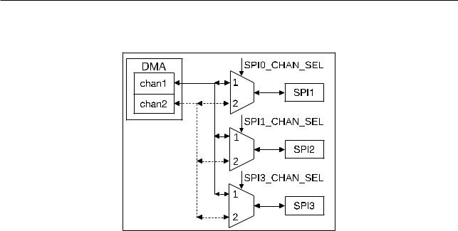
Figure 64. SPI DMA
ESP32 SPI modules can use DMA as well as the CPU for data exchange with peripherals. As can be seen from Figure 6-4, two DMA channels are shared by SPI1, SPI2 and SPI3 controllers. Each DMA channel can be used by any one SPI controller at any given time.
The ESP32 SPI DMA Engine also uses a linked list to receive/transmit data. Burst transmission is supported. The data size for a single transfer must be four bytes aligned. Consecutive data transfer is also supported.
SPI1_DMA_CHAN_SEL[1:0], SPI2_DMA_CHAN_SEL[1:0] and SPI3_DMA_CHAN_SEL[1:0] in DPORT_SPI_DMA_ CHAN_SEL_REG must be configured to enable the SPI DMA interface for a specific SPI controller. Each SPI controller corresponds to one domain which has two bits with values 0, 1 and 2. Value 3 is reserved and must not be configured for operation.
Considering SPI1 as an example,
if SPI SPI1_DMA_CHAN_SEL[1:0] = 0, then SPI1 does not use any DMA channel; if SPI1_DMA_CHAN_SEL[1:0] = 1, then SPI1 enables DMA channel1;
if SPI1_DMA_CHAN_SEL[1:0] = 2, then SPI1 enables DMA channel2.
The SPI_OUTLINK_START bit in SPI_DMA_OUT_LINK_REG and the SPI_INLINK_START bit in SPI_DMA_IN_LINK_REG are used for enabling the DMA Engine. The two bits are self-cleared by hardware. When SPI_OUTLINK_START
is set to 1, the DMA Engine starts processing the outbound linked list descriptor and prepares to transmit data. When SPI_INLINK_START is set to 1, then the DMA Engine starts processing the inbound linked-list descriptor and gets prepared to receive data.
Software should configure the SPI DMA as follows:
1.Reset the DMA state machine and FIFO parameters;
2.Configure the DMA-related registers for operation;
3.Configure the SPI-controller-related registers accordingly;
4.Set SPI_USR to enable DMA operation.
Espressif Systems |
123 |
ESP32 TRM (Version 5.0) |
Submit Documentation Feedback

6 DMA Controller (DMA)
6.6I2S DMA Interface
The ESP32 integrates two I2S modules, I2S0 and I2S1, each of which is powered by a DMA channel. The REG_I2S_DSCR_EN bit in I2S_FIFO_CONF_REG is used for enabling the DMA operation. ESP32 I2S DMA uses the standard linked-list descriptor to configure DMA operations for data transfer. Burst transfer is supported. However, unlike the SPI DMA channels, the data size for a single transfer is one word, or four bytes. REG_I2S_RX_EOF_NUM[31:0] bit in I2S_RXEOF_NUM_REG is used for configuring the data size of a single transfer operation, in multiples of one word.
I2S_OUTLINK_START bit in I2S_OUT_LINK_REG and I2S_INLINK_START bit in I2S_IN_LINK_REG are used for enabling the DMA Engine and are self-cleared by hardware. When I2S_OUTLINK_START is set to 1, the DMA Engine starts processing the outbound linked-list descriptor and gets prepared to send data. When I2S_INLINK_START is set to 1, the DMA Engine starts processing the inbound linked-list descriptor and gets prepared to receive data.
Software should configure the I2S DMA as follows:
1.Configure I2S-controller-related registers;
2.Reset the DMA state machine and FIFO parameters;
3.Configure DMA-related registers for operation;
4.In I2S master mode, set I2S_TX_START bit or I2S_RX_START bit to initiate an I2S operation;
In I2S slave mode, set I2S_TX_START bit or I2S_RX_START bit and wait for data transfer to be initiated by the host device.
For more information on I2S DMA interrupts, please see Section DMA Interrupts, in Chapter I2S.
Espressif Systems |
124 |
ESP32 TRM (Version 5.0) |
Submit Documentation Feedback