

- •1 System and Memory
- •1.1 Introduction
- •1.2 Features
- •1.3 Functional Description
- •1.3.1 Address Mapping
- •1.3.2 Embedded Memory
- •1.3.3 External Memory
- •1.3.5 Peripherals
- •2 Interrupt Matrix (INTERRUPT)
- •2.1 Overview
- •2.2 Features
- •2.3 Functional Description
- •2.3.1 Peripheral Interrupt Source
- •2.3.2 CPU Interrupt
- •2.3.3 Allocate Peripheral Interrupt Sources to Peripheral Interrupt on CPU
- •2.3.4 CPU NMI Interrupt Mask
- •2.3.5 Query Current Interrupt Status of Peripheral Interrupt Source
- •2.4 Registers
- •3 Reset and Clock
- •3.1 System Reset
- •3.1.1 Introduction
- •3.1.2 Reset Source
- •3.2 System Clock
- •3.2.1 Introduction
- •3.2.3 CPU Clock
- •3.2.4 Peripheral Clock
- •3.2.7 Audio PLL
- •3.3 Register Summary
- •3.4 Registers
- •4.1 Overview
- •4.2 Peripheral Input via GPIO Matrix
- •4.2.1 Summary
- •4.2.2 Functional Description
- •4.2.3 Simple GPIO Input
- •4.3 Peripheral Output via GPIO Matrix
- •4.3.1 Summary
- •4.3.3 Simple GPIO Output
- •4.4 Direct I/O via IO_MUX
- •4.4.1 Summary
- •4.4.2 Functional Description
- •4.5 RTC IO_MUX for Low Power and Analog I/O
- •4.5.1 Summary
- •4.5.2 Analog Function Description
- •4.7 Pad Hold Feature
- •4.8 I/O Pad Power Supplies
- •4.8.1 VDD_SDIO Power Domain
- •4.9 Peripheral Signal List
- •4.10 IO_MUX Pad List
- •4.11 RTC_MUX Pin List
- •4.12 Register Summary
- •4.12.1 GPIO Matrix Register Summary
- •4.12.2 IO MUX Register Summary
- •4.12.3 RTC IO MUX Register Summary
- •4.13 Registers
- •4.13.1 GPIO Matrix Registers
- •4.13.2 IO MUX Registers
- •4.13.3 RTC IO MUX Registers
- •5 DPort Registers
- •5.1 Introduction
- •5.2 Features
- •5.3 Functional Description
- •5.3.1 System and Memory Register
- •5.3.2 Reset and Clock Registers
- •5.3.3 Interrupt Matrix Register
- •5.3.4 DMA Registers
- •5.3.5 MPU/MMU Registers
- •5.3.7 Peripheral Clock Gating and Reset
- •5.4 Register Summary
- •5.5 Registers
- •6 DMA Controller (DMA)
- •6.1 Overview
- •6.2 Features
- •6.3 Functional Description
- •6.3.1 DMA Engine Architecture
- •6.3.2 Linked List
- •6.4 UART DMA (UDMA)
- •7 SPI Controller (SPI)
- •7.1 Overview
- •7.5 Parallel QSPI
- •7.5.1 Communication Format of Parallel QSPI
- •7.6.1 SPI Interrupts
- •7.6.2 DMA Interrupts
- •7.7 Register Summary
- •7.8 Registers
- •8 SDIO Slave Controller
- •8.1 Overview
- •8.2 Features
- •8.3 Functional Description
- •8.3.1 SDIO Slave Block Diagram
- •8.3.3 Register Access
- •8.3.6 SDIO Bus Timing
- •8.3.7 Interrupt
- •8.4 Register Summary
- •8.5 SLC Registers
- •8.6 SLC Host Registers
- •8.7 HINF Registers
- •9 SD/MMC Host Controller
- •9.1 Overview
- •9.2 Features
- •9.3 SD/MMC External Interface Signals
- •9.4 Functional Description
- •9.4.1 SD/MMC Host Controller Architecture
- •9.4.2 Command Path
- •9.4.3 Data Path
- •9.5 Software Restrictions for Proper CIU Operation
- •9.6 RAM for Receiving and Sending Data
- •9.6.1 Transmit RAM Module
- •9.6.2 Receive RAM Module
- •9.8 The Structure of a Linked List
- •9.9 Initialization
- •9.9.1 DMAC Initialization
- •9.9.2 DMAC Transmission Initialization
- •9.9.3 DMAC Reception Initialization
- •9.11 Interrupt
- •9.12 Register Summary
- •9.13 Registers
- •10 Ethernet Media Access Controller (MAC)
- •10.1 Overview
- •10.2 EMAC_CORE
- •10.2.1 Transmit Operation
- •10.2.2 Receive Operation
- •10.3 MAC Interrupt Controller
- •10.4 MAC Address Filtering
- •10.4.1 Unicast Destination Address Filtering
- •10.4.2 Multicast Destination Address Filtering
- •10.4.3 Broadcast Address Filtering
- •10.4.4 Unicast Source Address Filtering
- •10.4.5 Inverse Filtering Operation
- •10.4.6 Good Transmitted Frames and Received Frames
- •10.5 EMAC_MTL (MAC Transaction Layer)
- •10.6 PHY Interface
- •10.6.1 MII (Media Independent Interface)
- •10.6.3 Station Management Agent (SMA) Interface
- •10.6.4 RMII Timing
- •10.7 Ethernet DMA Features
- •10.8 Linked List Descriptors
- •10.8.1 Transmit Descriptors
- •10.8.2 Receive Descriptors
- •10.9 Register Summary
- •10.10 Registers
- •11 I2C Controller (I2C)
- •11.1 Overview
- •11.2 Features
- •11.3 Functional Description
- •11.3.1 Introduction
- •11.3.2 Architecture
- •11.3.3 I2C Bus Timing
- •11.3.7 Interrupts
- •11.4 Register Summary
- •11.5 Registers
- •12 I2S Controller (I2S)
- •12.1 Overview
- •12.2 Features
- •12.3 The Clock of I2S Module
- •12.4 I2S Mode
- •12.4.1 Supported Audio Standards
- •12.4.2 Module Reset
- •12.4.3 FIFO Operation
- •12.4.5 Receiving Data
- •12.5.1 LCD Master Transmitting Mode
- •12.5.2 Camera Slave Receiving Mode
- •12.5.3 ADC/DAC mode
- •12.6 I2S Interrupts
- •12.6.1 FIFO Interrupts
- •12.6.2 DMA Interrupts
- •12.7 Register Summary
- •12.8 Registers
- •13 UART Controller (UART)
- •13.1 Overview
- •13.2 UART Features
- •13.3 Functional Description
- •13.3.1 Introduction
- •13.3.3 UART RAM
- •13.3.5 UART Data Frame
- •13.3.7 Flow Control
- •13.3.8 UART DMA
- •13.3.9 UART Interrupts
- •13.3.10 UHCI Interrupts
- •13.4 Register Summary
- •13.4.1 UART Register Summary
- •13.5 Registers
- •13.5.1 UART Registers
- •13.5.2 UHCI Registers
- •14 LED PWM Controller (LEDC)
- •14.1 Introduction
- •14.2 Functional Description
- •14.2.1 Architecture
- •14.2.3 Channels
- •14.2.4 Interrupts
- •14.3 Register Summary
- •14.4 Registers
- •15 Remote Control Peripheral (RMT)
- •15.1 Introduction
- •15.2 Functional Description
- •15.2.1 RMT Architecture
- •15.2.3 Clock
- •15.2.4 Transmitter
- •15.2.5 Receiver
- •15.2.6 Interrupts
- •15.3 Register Summary
- •15.4 Registers
- •16 Motor Control PWM (PWM)
- •16.1 Introduction
- •16.2 Features
- •16.3 Submodules
- •16.3.1 Overview
- •16.3.2 PWM Timer Submodule
- •16.3.3 PWM Operator Submodule
- •16.3.4 Capture Submodule
- •16.4 Register Summary
- •16.5 Registers
- •17 Pulse Count Controller (PCNT)
- •17.1 Overview
- •17.2 Functional Description
- •17.2.1 Architecture
- •17.2.2 Counter Channel Inputs
- •17.2.3 Watchpoints
- •17.2.4 Examples
- •17.2.5 Interrupts
- •18 Timer Group (TIMG)
- •18.1 Introduction
- •18.2 Functional Description
- •18.2.2 64-bit Time-base Counter
- •18.2.3 Alarm Generation
- •18.2.4 MWDT
- •18.2.5 Interrupts
- •18.3 Register Summary
- •18.4 Registers
- •19 Watchdog Timers (WDT)
- •19.1 Introduction
- •19.2 Features
- •19.3 Functional Description
- •19.3.1 Clock
- •20 eFuse Controller
- •20.1 Introduction
- •20.2 Features
- •20.3 Functional Description
- •20.3.1 Structure
- •20.3.3 Software Reading of System Parameters
- •20.3.4 The Use of System Parameters by Hardware Modules
- •20.3.5 Interrupts
- •20.4 Register Summary
- •20.5 Registers
- •21 Two-wire Automotive Interface (TWAI)
- •21.1 Overview
- •21.2 Features
- •21.3 Functional Protocol
- •21.3.1 TWAI Properties
- •21.3.2 TWAI Messages
- •21.3.3 TWAI Errors
- •21.3.4 TWAI Bit Timing
- •21.4 Architectural Overview
- •21.4.1 Registers Block
- •21.4.2 Bit Stream Processor
- •21.4.3 Error Management Logic
- •21.4.4 Bit Timing Logic
- •21.4.5 Acceptance Filter
- •21.5 Functional Description
- •21.5.1 Modes
- •21.5.2 Bit Timing
- •21.5.3 Interrupt Management
- •21.5.4 Transmit and Receive Buffers
- •21.5.5 Receive FIFO and Data Overruns
- •21.5.6 Acceptance Filter
- •21.5.8 Error Code Capture
- •21.5.9 Arbitration Lost Capture
- •21.6 Register Summary
- •21.7 Registers
- •22 AES Accelerator (AES)
- •22.1 Introduction
- •22.2 Features
- •22.3 Functional Description
- •22.3.1 AES Algorithm Operations
- •22.3.2 Key, Plaintext and Ciphertext
- •22.3.3 Endianness
- •22.3.4 Encryption and Decryption Operations
- •22.3.5 Speed
- •22.4 Register Summary
- •22.5 Registers
- •23 SHA Accelerator (SHA)
- •23.1 Introduction
- •23.2 Features
- •23.3 Functional Description
- •23.3.1 Padding and Parsing the Message
- •23.3.2 Message Digest
- •23.3.3 Hash Operation
- •23.3.4 Speed
- •23.4 Register Summary
- •23.5 Registers
- •24 RSA Accelerator (RSA)
- •24.1 Introduction
- •24.2 Features
- •24.3 Functional Description
- •24.3.1 Initialization
- •24.3.2 Large Number Modular Exponentiation
- •24.3.4 Large Number Multiplication
- •24.4 Register Summary
- •24.5 Registers
- •25 Random Number Generator (RNG)
- •25.1 Introduction
- •25.2 Feature
- •25.3 Functional Description
- •25.5 Register Summary
- •25.6 Register
- •26 External Memory Encryption and Decryption (FLASH)
- •26.1 Overview
- •26.2 Features
- •26.3 Functional Description
- •26.3.1 Key Generator
- •26.3.2 Flash Encryption Block
- •26.3.3 Flash Decryption Block
- •26.4 Register Summary
- •26.5 Register
- •27 Memory Management and Protection Units (MMU, MPU)
- •27.1 Introduction
- •27.2 Features
- •27.3 Functional Description
- •27.3.1 PID Controller
- •28 Process ID Controller (PID)
- •28.1 Overview
- •28.2 Features
- •28.3 Functional Description
- •28.3.1 Interrupt Identification
- •28.3.2 Information Recording
- •28.3.3 Proactive Process Switching
- •28.4 Register Summary
- •28.5 Registers
- •29 On-Chip Sensors and Analog Signal Processing
- •29.1 Introduction
- •29.2 Capacitive Touch Sensor
- •29.2.1 Introduction
- •29.2.2 Features
- •29.2.3 Available GPIOs
- •29.2.4 Functional Description
- •29.2.5 Touch FSM
- •29.3.1 Introduction
- •29.3.2 Features
- •29.3.3 Outline of Function
- •29.3.4 RTC SAR ADC Controllers
- •29.3.5 DIG SAR ADC Controllers
- •29.4.1 Introduction
- •29.4.2 Features
- •29.4.4 Cosine Waveform Generator
- •29.5 Register Summary
- •29.5.1 Sensors
- •29.5.2 Advanced Peripheral Bus
- •29.6 Registers
- •29.6.1 Sensors
- •29.6.2 Advanced Peripheral Bus
- •30 ULP Coprocessor (ULP)
- •30.1 Introduction
- •30.2 Features
- •30.4 Instruction Set
- •30.4.2 ST – Store Data in Memory
- •30.4.3 LD – Load Data from Memory
- •30.4.4 JUMP – Jump to an Absolute Address
- •30.4.5 JUMPR – Jump to a Relative Offset (Conditional upon R0)
- •30.4.7 HALT – End the Program
- •30.4.8 WAKE – Wake up the Chip
- •30.4.10 WAIT – Wait for a Number of Cycles
- •30.4.12 I2C_RD/I2C_WR – Read/Write I²C
- •30.4.13 REG_RD – Read from Peripheral Register
- •30.5 ULP Program Execution
- •30.6 RTC_I2C Controller
- •30.6.1 Configuring RTC_I2C
- •30.6.2 Using RTC_I2C
- •30.7 Register Summary
- •30.7.1 SENS_ULP Address Space
- •30.7.2 RTC_I2C Address Space
- •30.8 Registers
- •30.8.1 SENS_ULP Address Space
- •30.8.2 RTC_I2C Address Space
- •31 Low-Power Management (RTC_CNTL)
- •31.1 Introduction
- •31.2 Features
- •31.3 Functional Description
- •31.3.2 Digital Core Voltage Regulator
- •31.3.4 Flash Voltage Regulator
- •31.3.5 Brownout Detector
- •31.3.6 RTC Module
- •31.3.9 Predefined Power Modes
- •31.3.10 Wakeup Source
- •31.3.12 RTC Timer
- •31.3.13 RTC Boot
- •31.4 Register Summary
- •31.5 Registers
- •Glossary
- •Abbreviations for Peripherals
- •Abbreviations for Registers
- •Revision History

31 Low-Power Management (RTC_CNTL)
|
ROM |
ON |
OFF |
OFF |
Y |
Y |
- |
|
|
|
|
|
|
|
|
|
|
|
Internal SRAM |
ON |
OFF |
OFF |
Y |
Y |
7 |
|
|
|
|
|
|
|
|
|
|
|
40 MHz Crystal |
ON |
OFF |
OFF |
Y |
Y |
- |
|
|
|
|
|
|
|
|
|
|
Analog |
PLL |
ON |
OFF |
OFF |
Y |
Y |
- |
|
|
|
|
|
|
|
|
||
8 MHz OSC |
ON |
OFF |
OFF |
Y |
Y |
- |
||
|
||||||||
|
|
|
|
|
|
|
|
|
|
Radio |
- |
- |
- |
Y |
Y |
- |
|
|
|
|
|
|
|
|
|
Notes*:
1.The power-domain RTC core is the “always-on” power domain, and the FPU/FPD option is not available.
2.The power-domain RTC peripherals include most of the fast logic in RTC, including the ULP co-processor, sensor controllers, etc.
3.The power-domain RTC slow memory should be forced to power on when it is used as retention memory, or when the ULP co-processor is working.
4.The power-domain RTC fast memory should be forced to power on, when it is used as retention memory.
5.When the power-domain digital core is powered down, all included in power domains are powered down.
6.The power-domain Wi-Fi includes the Wi-Fi MAC and BB.
7.Each internal SRAM can be power-gated independently.
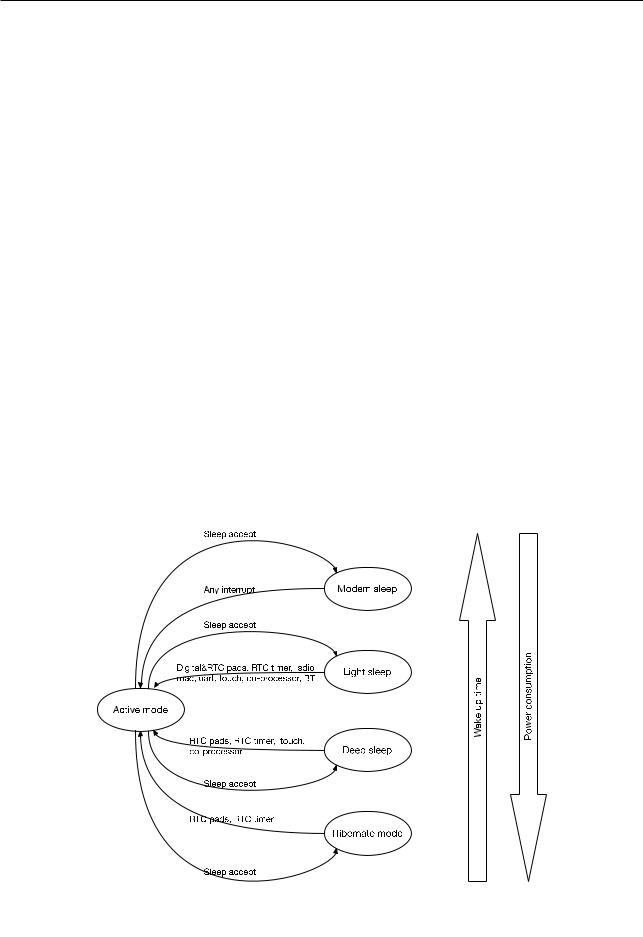
31.3.9 Predefined Power Modes
In ESP32, we recommend that you always use the predefined power modes first, before trying to tune each power
control signal. The predefined power modes should cover most scenarios:
•Active mode
–The CPU is clocked at XTAL_DIV_N (40 MHz/26 MHz) or PLL (80 MHz/160 MHz/240 MHz).
–The chip can receive, transmit, or listen.
•Modem-sleep mode
–The CPU is operational and the clock is configurable.
–The Wi-Fi/Bluetooth baseband is clock-gated or powered down. The radio is turned off.
–Current consumption: 30 mA with 80 MHz PLL.
–Current consumption: 3 mA with 2 MHz XTAL.
–Immediate wake-up.
•Light-sleep mode
–The internal 8 MHz oscillator, 40 MHz high-speed crystal, PLL, and radio are disabled.
–The clock in the digital core is gated. The CPUs are stalled.
–The ULP coprocessor and touch controller can be periodically triggered by monitor sensors.
–Current consumption: 800 µA.
–Wake-up latency: less than 1 ms.
•Deep-sleep mode
–The internal 8 MHz oscillator, 40 MHz high-speed crystal, PLL and radio are disabled.
–The digital core is powered down. The CPU context is lost.
Espressif Systems |
687 |
ESP32 TRM (Version 5.0) |
Submit Documentation Feedback
31Low-Power Management (RTC_CNTL)
–The supply voltage to the RTC core drops to 0.7V.
–8 x 32 bits of data are kept in general-purpose retention registers.
–The RTC memory and fast RTC memory can be retained.
–Current consumption: 6.5 µA.
–Wake-up latency: less than 1 ms.
–Recommended for ultra-low-power infrequently-connected Wi-Fi/Bluetooth applications.
•Hibernatation mode
–The internal 8 MHz oscillator, 40 MHz high-speed crystal, PLL, and radio are disabled.
–The digital core is powered down. The CPU context is lost.
–The RTC peripheral domain is powered down.
–The supply voltage to the RTC core drops to 0.7V.
–8 x 32 bits of data are kept in general-purpose retention registers.
–The RTC memory and fast RTC memory are powered down.
–Current consumption: 4.5 µA.
–Wake-up source: RTC timer only.
–Wake-up latency: less than 1 ms.
–Recommended for ultra-low-power infrequently-connected Wi-Fi/Bluetooth applications.
Figure 3110. Power Modes
By default, the ESP32 is in active mode after a system reset.There are several low-power modes for saving power when the CPU does not need to be kept running, for example, when waiting for an external event. It is up to the
Espressif Systems |
688 |
ESP32 TRM (Version 5.0) |
Submit Documentation Feedback

31 Low-Power Management (RTC_CNTL)
user to select the mode that best balances power consumption, wake-up latency and available wake-up sources. For details, please see Figure 31-10.
Please note that the predefined power mode could be further optimized and adapted to any application.
31.3.10 Wakeup Source
The ESP32 supports various wake-up sources, which could wake up the CPU in different sleep modes. The wake-up source is determined by RTC_CNTL_WAKEUP_ENA, as shown in Table 31-2.
Table 312. Wakeup Source
WAKEUP_ENA |
Wakeup Source1 |
Lightsleep |
Deepsleep |
Hibernation |
0x1 |
EXT02 |
Y |
Y |
- |
0x2 |
EXT13 |
Y |
Y |
Y |
0x4 |
GPIO4 |
Y |
Y |
- |
0x8 |
RTC timer |
Y |
Y |
Y |
|
|
|
|
|
0x10 |
SDIO5 |
Y |
- |
- |
0x20 |
Wi-Fi6 |
Y |
- |
- |
0x40 |
UART0 7 |
Y |
- |
- |
0x80 |
UART1 7 |
Y |
- |
- |
0x100 |
TOUCH |
Y |
Y |
- |
|
|
|
|
|
0x200 |
ULP co-processor |
Y |
Y |
- |
|
|
|
|
|
0x400 |
BT 6 |
Y |
- |
- |
1All wakeup sources can also be configured as the causes to reject sleep, except UART.
2EXT0 can only wake up the chip in light-sleep/deep-sleep mode.
If RTC_CNTL_EXT_WAKEUP0_LV is 1, it is pad high-level triggered; otherwise, it is
low-level triggered. Users can set RTCIO_EXT_WAKEUP0_SEL[4:0] to select one of the RTC PADs to be the wake-up source.
3EXT1 is especially designed to wake up the chip from any sleep mode, and it also supports multiple pads’ combinations.
First, RTC_CNTL_EXT_WAKEUP1_SEL[17:0] should be configured with the bitmap of PADS selected as a wake-up source. Then, if RTC_CNTL_EXT_WAKEUP1_LV is 1, as long as one of the PADs is at high-voltage level, it can trigger a wake-up. However, if RTC_CNTL_EXT_WAKEUP1_LV is 0, it needs all selected PADs to be
at low-voltage level to trigger a wake-up.
4 In Deep-sleep mode, only RTC GPIOs (not DIGITAL GPIOs) can work as wakeup source.
5 Wake-up is triggered by receiving any SDIO command.
6To wake up the chip with a Wi-Fi or BT source, the power mode switches between the Active, Modemand Light-sleep modes. The CPU, Wi-Fi, Bluetooth, and radio are woken up at predetermined intervals to keep Wi-Fi/BT connections active.
7Wake-up is triggered when the number or positive edges of RxD signal is greater than or equal to (UART_ACTIVE_THRESHOLD+2). Note that the RxD signal cannot be input through GPIO Matrix but only through IO_MUX.
Espressif Systems |
689 |
ESP32 TRM (Version 5.0) |
Submit Documentation Feedback

31 Low-Power Management (RTC_CNTL)
31.3.11 Reject Sleep
ESP32 implements a hardware mechanism that equips the chip with the ability to reject to sleep, which prevents the chip from going to sleep unexpectedly when some peripherals are still working but not detected by the CPU, thus guaranteeing the proper functioning of the peripherals.
All the wakeup sources specified in Table 31-2 (except UART) can also be configured as the causes to reject sleep.
Users can configure the reject to sleep option via the following registers.
•Configure the RTC_CNTL_SLP_REJECT field to enable or disable the option to reject to sleep:
–Set RTC_CNTL_LIGHT_SLP_REJECT_EN to enable reject-to-light-sleep.
–Set RTC_CNTL_DEEP_SLP_REJECT_EN to enable reject-to-deep-sleep.
•Read RTC_CNTL_REJECT_CAUSE to check the reason for rejecting to sleep.
31.3.12 RTC Timer
The RTC timer is a 48-bit counter that can be read. The clock is RTC_SLOW_CLK. Any reset/sleep mode, except for the power-up reset, will not stop or reset the RTC timer.
The RTC timer can be used to wake up the CPU at a designated time, and to wake up TOUCH or the ULP coprocessor periodically.
31.3.13 RTC Boot
Since the CPU, ROM and RAM are powered down during Deep-sleep and Hibernation mode, the wake-up time is much longer than that in Light sleep/Modem sleep, because of the ROM unpacking and data-copying from the flash (SPI booting). There are two types of SRAM in the RTC, named slow RTC memory and fast RTC memory, which remain powered-on in Deep-sleep mode. For small-scale codes (less than 8 KB), there are two methods of speeding up the wake-up time, i.e. avoiding ROM unpacking and SPI booting.
The first method is to use the RTC slow memory:
1.Set register RTC_CNTL_PROCPU_STAT_VECTOR_SEL for PRO_CPU (or register RTC_CNTL_APPCPU_STAT_VECTOR_ for APP_CPU) to 0.
2.Put the chip into sleep.
3.When the CPU is powered up, the reset vector starts from 0x50000000, instead of 0x40000400. ROM unpacking & SPI boot are not needed. The code in RTC memory has to do itself some initialization for the C program environment.
The second method is to use the fast RTC memory:
1.Set register RTC_CNTL_PROCPU_STAT_VECTOR_SEL for PRO_CPU (or register RTC_CNTL_APPCPU_STAT_VECTOR_ for APP_CPU) to 1.
2.Calculate CRC for the fast RTC memory, and save the result in register RTC_CNTL_RTC_STORE6_REG[31:0].
3.Input register RTC_CNTL_RTC_STORE7_REG[31:0] with the entry address in the fast RTC memory.
4.Put the chip into sleep.
5.When the CPU is powered up, after ROM unpacking and some necessary initialization, the CRC is calculated again. If the result matches with register RTC_CNTL_RTC_STORE6_REG[31:0], the CPU will jump to the
Espressif Systems |
690 |
ESP32 TRM (Version 5.0) |
Submit Documentation Feedback