

- •1 System and Memory
- •1.1 Introduction
- •1.2 Features
- •1.3 Functional Description
- •1.3.1 Address Mapping
- •1.3.2 Embedded Memory
- •1.3.3 External Memory
- •1.3.5 Peripherals
- •2 Interrupt Matrix (INTERRUPT)
- •2.1 Overview
- •2.2 Features
- •2.3 Functional Description
- •2.3.1 Peripheral Interrupt Source
- •2.3.2 CPU Interrupt
- •2.3.3 Allocate Peripheral Interrupt Sources to Peripheral Interrupt on CPU
- •2.3.4 CPU NMI Interrupt Mask
- •2.3.5 Query Current Interrupt Status of Peripheral Interrupt Source
- •2.4 Registers
- •3 Reset and Clock
- •3.1 System Reset
- •3.1.1 Introduction
- •3.1.2 Reset Source
- •3.2 System Clock
- •3.2.1 Introduction
- •3.2.3 CPU Clock
- •3.2.4 Peripheral Clock
- •3.2.7 Audio PLL
- •3.3 Register Summary
- •3.4 Registers
- •4.1 Overview
- •4.2 Peripheral Input via GPIO Matrix
- •4.2.1 Summary
- •4.2.2 Functional Description
- •4.2.3 Simple GPIO Input
- •4.3 Peripheral Output via GPIO Matrix
- •4.3.1 Summary
- •4.3.3 Simple GPIO Output
- •4.4 Direct I/O via IO_MUX
- •4.4.1 Summary
- •4.4.2 Functional Description
- •4.5 RTC IO_MUX for Low Power and Analog I/O
- •4.5.1 Summary
- •4.5.2 Analog Function Description
- •4.7 Pad Hold Feature
- •4.8 I/O Pad Power Supplies
- •4.8.1 VDD_SDIO Power Domain
- •4.9 Peripheral Signal List
- •4.10 IO_MUX Pad List
- •4.11 RTC_MUX Pin List
- •4.12 Register Summary
- •4.12.1 GPIO Matrix Register Summary
- •4.12.2 IO MUX Register Summary
- •4.12.3 RTC IO MUX Register Summary
- •4.13 Registers
- •4.13.1 GPIO Matrix Registers
- •4.13.2 IO MUX Registers
- •4.13.3 RTC IO MUX Registers
- •5 DPort Registers
- •5.1 Introduction
- •5.2 Features
- •5.3 Functional Description
- •5.3.1 System and Memory Register
- •5.3.2 Reset and Clock Registers
- •5.3.3 Interrupt Matrix Register
- •5.3.4 DMA Registers
- •5.3.5 MPU/MMU Registers
- •5.3.7 Peripheral Clock Gating and Reset
- •5.4 Register Summary
- •5.5 Registers
- •6 DMA Controller (DMA)
- •6.1 Overview
- •6.2 Features
- •6.3 Functional Description
- •6.3.1 DMA Engine Architecture
- •6.3.2 Linked List
- •6.4 UART DMA (UDMA)
- •7 SPI Controller (SPI)
- •7.1 Overview
- •7.5 Parallel QSPI
- •7.5.1 Communication Format of Parallel QSPI
- •7.6.1 SPI Interrupts
- •7.6.2 DMA Interrupts
- •7.7 Register Summary
- •7.8 Registers
- •8 SDIO Slave Controller
- •8.1 Overview
- •8.2 Features
- •8.3 Functional Description
- •8.3.1 SDIO Slave Block Diagram
- •8.3.3 Register Access
- •8.3.6 SDIO Bus Timing
- •8.3.7 Interrupt
- •8.4 Register Summary
- •8.5 SLC Registers
- •8.6 SLC Host Registers
- •8.7 HINF Registers
- •9 SD/MMC Host Controller
- •9.1 Overview
- •9.2 Features
- •9.3 SD/MMC External Interface Signals
- •9.4 Functional Description
- •9.4.1 SD/MMC Host Controller Architecture
- •9.4.2 Command Path
- •9.4.3 Data Path
- •9.5 Software Restrictions for Proper CIU Operation
- •9.6 RAM for Receiving and Sending Data
- •9.6.1 Transmit RAM Module
- •9.6.2 Receive RAM Module
- •9.8 The Structure of a Linked List
- •9.9 Initialization
- •9.9.1 DMAC Initialization
- •9.9.2 DMAC Transmission Initialization
- •9.9.3 DMAC Reception Initialization
- •9.11 Interrupt
- •9.12 Register Summary
- •9.13 Registers
- •10 Ethernet Media Access Controller (MAC)
- •10.1 Overview
- •10.2 EMAC_CORE
- •10.2.1 Transmit Operation
- •10.2.2 Receive Operation
- •10.3 MAC Interrupt Controller
- •10.4 MAC Address Filtering
- •10.4.1 Unicast Destination Address Filtering
- •10.4.2 Multicast Destination Address Filtering
- •10.4.3 Broadcast Address Filtering
- •10.4.4 Unicast Source Address Filtering
- •10.4.5 Inverse Filtering Operation
- •10.4.6 Good Transmitted Frames and Received Frames
- •10.5 EMAC_MTL (MAC Transaction Layer)
- •10.6 PHY Interface
- •10.6.1 MII (Media Independent Interface)
- •10.6.3 Station Management Agent (SMA) Interface
- •10.6.4 RMII Timing
- •10.7 Ethernet DMA Features
- •10.8 Linked List Descriptors
- •10.8.1 Transmit Descriptors
- •10.8.2 Receive Descriptors
- •10.9 Register Summary
- •10.10 Registers
- •11 I2C Controller (I2C)
- •11.1 Overview
- •11.2 Features
- •11.3 Functional Description
- •11.3.1 Introduction
- •11.3.2 Architecture
- •11.3.3 I2C Bus Timing
- •11.3.7 Interrupts
- •11.4 Register Summary
- •11.5 Registers
- •12 I2S Controller (I2S)
- •12.1 Overview
- •12.2 Features
- •12.3 The Clock of I2S Module
- •12.4 I2S Mode
- •12.4.1 Supported Audio Standards
- •12.4.2 Module Reset
- •12.4.3 FIFO Operation
- •12.4.5 Receiving Data
- •12.5.1 LCD Master Transmitting Mode
- •12.5.2 Camera Slave Receiving Mode
- •12.5.3 ADC/DAC mode
- •12.6 I2S Interrupts
- •12.6.1 FIFO Interrupts
- •12.6.2 DMA Interrupts
- •12.7 Register Summary
- •12.8 Registers
- •13 UART Controller (UART)
- •13.1 Overview
- •13.2 UART Features
- •13.3 Functional Description
- •13.3.1 Introduction
- •13.3.3 UART RAM
- •13.3.5 UART Data Frame
- •13.3.7 Flow Control
- •13.3.8 UART DMA
- •13.3.9 UART Interrupts
- •13.3.10 UHCI Interrupts
- •13.4 Register Summary
- •13.4.1 UART Register Summary
- •13.5 Registers
- •13.5.1 UART Registers
- •13.5.2 UHCI Registers
- •14 LED PWM Controller (LEDC)
- •14.1 Introduction
- •14.2 Functional Description
- •14.2.1 Architecture
- •14.2.3 Channels
- •14.2.4 Interrupts
- •14.3 Register Summary
- •14.4 Registers
- •15 Remote Control Peripheral (RMT)
- •15.1 Introduction
- •15.2 Functional Description
- •15.2.1 RMT Architecture
- •15.2.3 Clock
- •15.2.4 Transmitter
- •15.2.5 Receiver
- •15.2.6 Interrupts
- •15.3 Register Summary
- •15.4 Registers
- •16 Motor Control PWM (PWM)
- •16.1 Introduction
- •16.2 Features
- •16.3 Submodules
- •16.3.1 Overview
- •16.3.2 PWM Timer Submodule
- •16.3.3 PWM Operator Submodule
- •16.3.4 Capture Submodule
- •16.4 Register Summary
- •16.5 Registers
- •17 Pulse Count Controller (PCNT)
- •17.1 Overview
- •17.2 Functional Description
- •17.2.1 Architecture
- •17.2.2 Counter Channel Inputs
- •17.2.3 Watchpoints
- •17.2.4 Examples
- •17.2.5 Interrupts
- •18 Timer Group (TIMG)
- •18.1 Introduction
- •18.2 Functional Description
- •18.2.2 64-bit Time-base Counter
- •18.2.3 Alarm Generation
- •18.2.4 MWDT
- •18.2.5 Interrupts
- •18.3 Register Summary
- •18.4 Registers
- •19 Watchdog Timers (WDT)
- •19.1 Introduction
- •19.2 Features
- •19.3 Functional Description
- •19.3.1 Clock
- •20 eFuse Controller
- •20.1 Introduction
- •20.2 Features
- •20.3 Functional Description
- •20.3.1 Structure
- •20.3.3 Software Reading of System Parameters
- •20.3.4 The Use of System Parameters by Hardware Modules
- •20.3.5 Interrupts
- •20.4 Register Summary
- •20.5 Registers
- •21 Two-wire Automotive Interface (TWAI)
- •21.1 Overview
- •21.2 Features
- •21.3 Functional Protocol
- •21.3.1 TWAI Properties
- •21.3.2 TWAI Messages
- •21.3.3 TWAI Errors
- •21.3.4 TWAI Bit Timing
- •21.4 Architectural Overview
- •21.4.1 Registers Block
- •21.4.2 Bit Stream Processor
- •21.4.3 Error Management Logic
- •21.4.4 Bit Timing Logic
- •21.4.5 Acceptance Filter
- •21.5 Functional Description
- •21.5.1 Modes
- •21.5.2 Bit Timing
- •21.5.3 Interrupt Management
- •21.5.4 Transmit and Receive Buffers
- •21.5.5 Receive FIFO and Data Overruns
- •21.5.6 Acceptance Filter
- •21.5.8 Error Code Capture
- •21.5.9 Arbitration Lost Capture
- •21.6 Register Summary
- •21.7 Registers
- •22 AES Accelerator (AES)
- •22.1 Introduction
- •22.2 Features
- •22.3 Functional Description
- •22.3.1 AES Algorithm Operations
- •22.3.2 Key, Plaintext and Ciphertext
- •22.3.3 Endianness
- •22.3.4 Encryption and Decryption Operations
- •22.3.5 Speed
- •22.4 Register Summary
- •22.5 Registers
- •23 SHA Accelerator (SHA)
- •23.1 Introduction
- •23.2 Features
- •23.3 Functional Description
- •23.3.1 Padding and Parsing the Message
- •23.3.2 Message Digest
- •23.3.3 Hash Operation
- •23.3.4 Speed
- •23.4 Register Summary
- •23.5 Registers
- •24 RSA Accelerator (RSA)
- •24.1 Introduction
- •24.2 Features
- •24.3 Functional Description
- •24.3.1 Initialization
- •24.3.2 Large Number Modular Exponentiation
- •24.3.4 Large Number Multiplication
- •24.4 Register Summary
- •24.5 Registers
- •25 Random Number Generator (RNG)
- •25.1 Introduction
- •25.2 Feature
- •25.3 Functional Description
- •25.5 Register Summary
- •25.6 Register
- •26 External Memory Encryption and Decryption (FLASH)
- •26.1 Overview
- •26.2 Features
- •26.3 Functional Description
- •26.3.1 Key Generator
- •26.3.2 Flash Encryption Block
- •26.3.3 Flash Decryption Block
- •26.4 Register Summary
- •26.5 Register
- •27 Memory Management and Protection Units (MMU, MPU)
- •27.1 Introduction
- •27.2 Features
- •27.3 Functional Description
- •27.3.1 PID Controller
- •28 Process ID Controller (PID)
- •28.1 Overview
- •28.2 Features
- •28.3 Functional Description
- •28.3.1 Interrupt Identification
- •28.3.2 Information Recording
- •28.3.3 Proactive Process Switching
- •28.4 Register Summary
- •28.5 Registers
- •29 On-Chip Sensors and Analog Signal Processing
- •29.1 Introduction
- •29.2 Capacitive Touch Sensor
- •29.2.1 Introduction
- •29.2.2 Features
- •29.2.3 Available GPIOs
- •29.2.4 Functional Description
- •29.2.5 Touch FSM
- •29.3.1 Introduction
- •29.3.2 Features
- •29.3.3 Outline of Function
- •29.3.4 RTC SAR ADC Controllers
- •29.3.5 DIG SAR ADC Controllers
- •29.4.1 Introduction
- •29.4.2 Features
- •29.4.4 Cosine Waveform Generator
- •29.5 Register Summary
- •29.5.1 Sensors
- •29.5.2 Advanced Peripheral Bus
- •29.6 Registers
- •29.6.1 Sensors
- •29.6.2 Advanced Peripheral Bus
- •30 ULP Coprocessor (ULP)
- •30.1 Introduction
- •30.2 Features
- •30.4 Instruction Set
- •30.4.2 ST – Store Data in Memory
- •30.4.3 LD – Load Data from Memory
- •30.4.4 JUMP – Jump to an Absolute Address
- •30.4.5 JUMPR – Jump to a Relative Offset (Conditional upon R0)
- •30.4.7 HALT – End the Program
- •30.4.8 WAKE – Wake up the Chip
- •30.4.10 WAIT – Wait for a Number of Cycles
- •30.4.12 I2C_RD/I2C_WR – Read/Write I²C
- •30.4.13 REG_RD – Read from Peripheral Register
- •30.5 ULP Program Execution
- •30.6 RTC_I2C Controller
- •30.6.1 Configuring RTC_I2C
- •30.6.2 Using RTC_I2C
- •30.7 Register Summary
- •30.7.1 SENS_ULP Address Space
- •30.7.2 RTC_I2C Address Space
- •30.8 Registers
- •30.8.1 SENS_ULP Address Space
- •30.8.2 RTC_I2C Address Space
- •31 Low-Power Management (RTC_CNTL)
- •31.1 Introduction
- •31.2 Features
- •31.3 Functional Description
- •31.3.2 Digital Core Voltage Regulator
- •31.3.4 Flash Voltage Regulator
- •31.3.5 Brownout Detector
- •31.3.6 RTC Module
- •31.3.9 Predefined Power Modes
- •31.3.10 Wakeup Source
- •31.3.12 RTC Timer
- •31.3.13 RTC Boot
- •31.4 Register Summary
- •31.5 Registers
- •Glossary
- •Abbreviations for Peripherals
- •Abbreviations for Registers
- •Revision History

31 Low-Power Management (RTC_CNTL)
31 LowPower Management (RTC_CNTL)
31.1Introduction
ESP32 offers efficient and flexible power-management technology to achieve the best balance between power consumption, wakeup latency and available wakeup sources. Users can select out of five predefined power modes of the main processors to suit specific needs of the application. In addition, to save power in powersensitive applications, control may be executed by the Ultra-Low-Power coprocessor (ULP coprocessor), while the main processors are in Deep-sleep mode.
31.2Features
•Five predefined power modes to support various applications
•Up to 16 KB of retention memory
•8 x 32 bits of retention registers
•ULP coprocessor enabled in all low-power modes
•RTC boot supported to shorten the wakeup latency
Figure 311. ESP32 Power Control
31.3Functional Description
Espressif Systems |
680 |
ESP32 TRM (Version 5.0) |
Submit Documentation Feedback
31 Low-Power Management (RTC_CNTL)
31.3.1 Overview
The low-power management unit includes voltage regulators, a power controller, power switch cells, power domain isolation cells, etc. Figure 31-1 shows the high-level architecture of ESP32’s low-power management.
31.3.2 Digital Core Voltage Regulator
The built-in voltage regulator can convert the external power supply (typically 3.3V) to 1.1V to support the internal digital core. It receives a wide range of external power supply from 1.8V to 3.6V, and provides an output voltage from 0.90V to 1.25V.
1.When XPD_DIG_REG == 1, the regulator outputs a 1.1V voltage and the digital core is able to run; when XPD_DIG_REG == 0, both the regulator and the digital core stop running.
2.DIG_REG_DBIAS[2:0] tunes the supply voltage of the digital core:
VDD_DIG = 0.90 + DBIAS · 0.05V
3. The current to the digital core comes from pin VDD3P3_CPU and pin VDD3P3_RTC.
Figure 31-2 shows the structure of a digital core’s voltage regulator.
90 |
Figure 312. Digital Core Voltage Regulator
31.3.3 LowPower Voltage Regulator
The built-in low-power voltage regulator can convert the external power supply (typically 3.3V) to 1.1V to support the internal RTC core. To save power, it receives a wide range of external power supply from 1.8V to 3.6V, and supports an adjustable output voltage of 0.90V to 1.25V in normal work mode, a fixed output voltage of about 0.75V both in Deep-sleep mode and Hibernation mode.
1.When the pin CHIP_PU is at a high level, the low-power voltage regulator cannot be turned off. It should be switched only between normal-work mode and Deep-sleep mode.
Espressif Systems |
681 |
ESP32 TRM (Version 5.0) |
Submit Documentation Feedback

31Low-Power Management (RTC_CNTL)
2.In normal-work mode, RTC_DBIAS[2:0] can be used to tune the output voltage:
VDD_RTC = 0.90 + DBIAS · 0.05V
3.In Deep-sleep mode, the output voltage of the regulator is fixed at about 0.75V.
4.The current to the RTC core comes from pin VDD3P3_RTC.
Figure 31-3 shows the structure of a low-power voltage regulator.
90 |
Figure 313. LowPower Voltage Regulator
31.3.4 Flash Voltage Regulator
The built-in flash voltage regulator can supply a voltage of 3.3V or 1.8V to other devices (flash, for example) in the system, with a maximum output current of 40 mA.
1.When XPD_SDIO_VREG == 1, the regulator outputs a voltage of 3.3V or 1.8V; when XPD_SDIO_VREG == 0, the output is high-impedance and, in this case, the voltage is provided by the external power supply.
2.When SDIO_TIEH == 1, the regulator shorts pin VDD_SDIO to pin VDD3P3_RTC. The regulator then outputs a voltage of 3.3V which is the voltage of pin VDD3P3_RTC. When SDIO_TIEH == 0, the inner loop ties the regulator output to the voltage of VREF, which is typically 1.8V.
3.DREFH_SDIO, DREFM_SDIO and DREFL_SDIO could be used to tune the reference voltage VREF slightly. However, it is recommended that users do not change the value of these registers, since it may affect the stability of the inner loop.
4.When the regulator output is 3.3V or 1.8V, the output current comes from the pin VDD3P3_RTC.
Figure 31-4 shows the structure of a flash voltage regulator.
Espressif Systems |
682 |
ESP32 TRM (Version 5.0) |
Submit Documentation Feedback

31 Low-Power Management (RTC_CNTL)
Figure 314. Flash Voltage Regulator
31.3.5 Brownout Detector
The brownout detector checks the voltage of pin VDD3P3_RTC. If the voltage drops rapidly and becomes too low, the detector would trigger a signal to shut down some power-consuming blocks (such as LNA, PA, etc.) to allow extra time for the digital block to save and transfer important data. The power consumption of the detector is ultra low. It remains enabled whenever the chip is powered on, with an adjustable trigger level calibrated around 2.5V.
1.As the output of the brownout detector, RTC_CNTL_BROWN_OUT_DET goes high when the voltage of pin VDD3P3_RTC is lower than the threshold value.
2.RTC_CNTL_DBROWN_OUT_THRES[2:0] is used to tune the threshold voltage, which is usually calibrated around 2.5V.
Figure 31-5 shows the structure of a brownout detector.
Figure 315. Brownout Detector
31.3.6 RTC Module
The RTC module is designed to handle the entry into, and exit from, the low-power mode, and control the clock sources, PLL, power switch and isolation cells to generate power-gating, clock-gating, and reset signals. As for the low-power management, RTC is composed of the following modules (see Figure 31-6):
• RTC main state machine: records the power state.
Espressif Systems |
683 |
ESP32 TRM (Version 5.0) |
Submit Documentation Feedback

31Low-Power Management (RTC_CNTL)
•Digital & analog power controller: generates actual power-gating/clock-gating signals for digital parts and analog parts.
•Sleep & wakeup controller: handles the entry into & exit from the low-power mode.
•Timers: include RTC main timer, ULP coprocessor timer and touch timer.
•Low-Power processor and sensor controllers: include ULP coprocessor, touch controller, SAR ADC controller, etc.
•Retention memory:
–RTC slow memory: an 8 KB SRAM, mostly used as retention memory or instruction & data memory for the ULP coprocessor. The CPU accesses it through the APB, starting from address 0x50000000.
–RTC fast memory: an 8 KB SRAM, mostly used as retention memory. The CPU accesses it through IRAM0/DRAM0. Fast RTC memory is about 10 times faster than the RTC slow memory.
•Retention registers: always-on registers of 8 x 32 bits, serving as data storage.
•RTC IO pads: 18 always-on analog pads, usually functioning as wake-up sources.
Figure 316. RTC Structure
Espressif Systems |
684 |
ESP32 TRM (Version 5.0) |
Submit Documentation Feedback
31 Low-Power Management (RTC_CNTL)
31.3.7 LowPower Clocks
In the low-power mode, the 40 MHz crystal and PLL are usually powered down to save power. But clocks are needed for the chip to remain active in the low-power mode.
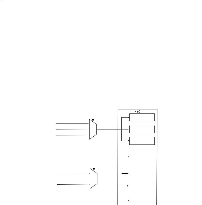
For the RTC core, there are five possible clock sources:
•external low-speed (32.768 kHz) crystal clock XTL32K_CLK,
•external high-speed (2 MHz ~ 40 MHz) crystal clock XTAL_DIV_CLK,
•internal RC oscillator RC_SLOW_CLK (typically about 150 kHz and adjustable),
•internal 8-MHz oscillator RC_FAST_CLK, and
•internal 31.25-kHz clock RC_FAST_DIV_CLK (derived from the internal 8-MHz oscillator divided by 256).
With while
RC_SLOW_CLK
XTL32K_CLK
RC_FAST_DIV_CLK
RTC Slow Clock
ESP32
Selection Signal
RTC Timer
 0
0
 1 RTC_SLOW_CLK
  RTC Main State
 2
2
PMU
|
Selection Signal |
|
|
ULP Coprocessor |
||
|
|
|
||||
|
|
|
|
|||
|
|
|
|
|||
XTAL_DIV_CLK |
|
|
|
|
|
|
|
|
|
|
|
|
|
|
|
|
|
|
|
|
0 |
|
|
|
|
Sensor Controller |
|
|
|
|
|
|
||
|
|
RTC_FAST_CLK |
|
|
|
|
RC_FAST_CLK |
1 |
|
|
|
|
|
|
|
|
|
|
||
|
|
|
|
RTC Memory |
||
|
|
|
|
|
||
RTC Fast Clock |
|
|
|
|
|
|
|
|
|
|
|
|
|
|
|
|
|
|
|
RTC Registers |
|
|
|
|
|
|
|
|
|
|
|
|
|
|
RTC Clock
Figure 317. RTC LowPower Clocks
For the digital core, LOW_POWERE_CLK is switched among four sources. For details, please see Figure 31- 8.
Espressif Systems |
685 |
ESP32 TRM (Version 5.0) |
Submit Documentation Feedback

RC_SLOW_CLK
RTC_SLOW_CLK
RC_FAST_CLK XTL_CLK
Selection Signals
MUX |
LOW_POWER_CLK |
|
|
|
|
Wireless |
|||
|
||||
LP |
|
|
|
Figure 318. Digital LowPower Clocks
Low-power Clock
31.3.8 PowerGating Implementation
Figure 319. RTC States
The switch among power-gating states can be see in Figure 31-9. The actual power-control signals could also be set by software as force-power-up (FPU) or force-power-down (FPD). Since the power domains can be powergated independently, there are many combinations for different applications. Table 31-1 shows how the power domains in ESP32 are controlled.
Table 311. RTC Power Domains
|
Power Domains |
|
RTC Main State |
|
S/W Options |
Notes* |
||
|
DIG Active |
RTC Active |
RTC Sleep |
FPU |
FPD |
|||
|
|
|
|
|||||
|
|
RTC Digital Core |
ON |
ON |
ON |
N |
N |
1 |
|
|
|
|
|
|
|
|
|
|
RTC |
RTC Peripherals |
ON |
ON |
OFF |
Y |
Y |
2 |
|
|
|
|
|
|
|
|
|
|
RTC Slow Memory |
ON |
OFF |
OFF |
Y |
Y |
3 |
|
|
|
|||||||
|
|
|
|
|
|
|
|
|
|
|
RTC Fast Memory |
ON |
OFF |
OFF |
Y |
Y |
4 |
|
|
|
|
|
|
|
|
|
|
|
Digital Core |
ON |
OFF |
OFF |
Y |
Y |
5 |
|
|
|
|
|
|
|
|
|
|
Digital |
Wi-Fi |
ON |
OFF |
OFF |
Y |
Y |
6 |
|
|
|
|
|
|
|
|
|
|
|
|
|
|
|
|
|
|
Espressif Systems |
|
686 |
|
ESP32 TRM (Version 5.0) |
||||
Submit Documentation Feedback