

ESP32
Technical Reference Manual
Version 5.0
Espressif Systems
Copyright © 2023
www.espressif.com
About This Manual
The ESP32 Technical Reference Manual is addressed to application developers. The manual provides detailed and complete information on how to use the ESP32 memory and peripherals.
For pin definition, electrical characteristics, and package information, please see ESP32 Datasheet.
Document Updates
Please always refer to the latest version at https://www.espressif.com/en/support/download/documents.
Revision History
For any changes to this document over time, please refer to the last page.
Documentation Change Notification
Espressif provides email notifications to keep customers updated on changes to technical documentation. Please subscribe at www.espressif.com/en/subscribe.
Certification
Download certificates for Espressif products from www.espressif.com/en/certificates.

Contents
Contents
1 |
System and Memory |
24 |
||
1.1 |
Introduction |
|
24 |
|
1.2 |
Features |
|
24 |
|
1.3 |
Functional Description |
26 |
||
|
1.3.1 |
Address Mapping |
26 |
|
|
1.3.2 |
Embedded Memory |
26 |
|
|
|
1.3.2.1 |
Internal ROM 0 |
27 |
|
|
1.3.2.2 |
Internal ROM 1 |
27 |
|
|
1.3.2.3 |
Internal SRAM 0 |
27 |
|
|
1.3.2.4 |
Internal SRAM 1 |
28 |
|
|
1.3.2.5 |
Internal SRAM 2 |
28 |
|
|
1.3.2.6 |
DMA |
29 |
|
|
1.3.2.7 |
RTC FAST Memory |
29 |
|
|
1.3.2.8 |
RTC SLOW Memory |
29 |
|
1.3.3 |
External Memory |
29 |
|
|
1.3.4 |
Cache |
|
30 |
|
1.3.5 |
Peripherals |
31 |
|
|
|
1.3.5.1 Asymmetric PID Controller Peripheral |
32 |
|
|
|
1.3.5.2 Non-Contiguous Peripheral Memory Ranges |
32 |
|
|
|
1.3.5.3 |
Memory Speed |
33 |
2 |
Interrupt Matrix (INTERRUPT) |
34 |
||
2.1 |
Overview |
|
34 |
|
2.2 |
Features |
|
34 |
|
2.3 |
Functional Description |
34 |
||
|
2.3.1 |
Peripheral Interrupt Source |
34 |
|
|
2.3.2 |
CPU Interrupt |
37 |
|
|
2.3.3 Allocate Peripheral Interrupt Sources to Peripheral Interrupt on CPU |
37 |
||
|
2.3.4 CPU NMI Interrupt Mask |
38 |
||
|
2.3.5 Query Current Interrupt Status of Peripheral Interrupt Source |
38 |
||
2.4 |
Registers |
|
38 |
|
3 |
Reset and Clock |
39 |
||
3.1 |
System Reset |
|
39 |
|
|
3.1.1 |
Introduction |
39 |
|
|
3.1.2 |
Reset Source |
39 |
|
3.2 |
System Clock |
|
40 |
|
|
3.2.1 |
Introduction |
40 |
|
|
3.2.2 |
Clock Source |
41 |
|
|
3.2.3 |
CPU Clock |
41 |
|
|
3.2.4 |
Peripheral Clock |
42 |
|
|
|
3.2.4.1 |
APB_CLK |
42 |
Espressif Systems |
3 |
ESP32 TRM (Version 5.0) |
||
Submit Documentation Feedback

Contents
|
|
3.2.4.2 |
REF_TICK |
42 |
|
|
3.2.4.3 |
LEDC_SCLK Source |
43 |
|
|
3.2.4.4 |
APLL_SCLK Source |
43 |
|
|
3.2.4.5 |
PLL_F160M_CLK Source |
43 |
|
|
3.2.4.6 |
Clock Source Considerations |
43 |
|
3.2.5 |
Wi-Fi BT Clock |
43 |
|
|
3.2.6 |
RTC Clock |
44 |
|
|
3.2.7 |
Audio PLL |
|
44 |
3.3 |
Register Summary |
|
44 |
|
3.4 |
Registers |
|
45 |
|
4 |
IO_MUX and GPIO Matrix (GPIO, IO_MUX) |
48 |
||
4.1 |
Overview |
|
48 |
|
4.2 |
Peripheral Input via GPIO Matrix |
|
49 |
|
|
4.2.1 |
Summary |
|
49 |
|
4.2.2 |
Functional Description |
|
49 |
|
4.2.3 |
Simple GPIO Input |
|
50 |
4.3 |
Peripheral Output via GPIO Matrix |
|
50 |
|
|
4.3.1 |
Summary |
|
50 |
|
4.3.2 |
Functional Description |
|
51 |
|
4.3.3 |
Simple GPIO Output |
|
52 |
4.4 |
Direct I/O via IO_MUX |
|
52 |
|
|
4.4.1 |
Summary |
|
52 |
|
4.4.2 |
Functional Description |
|
52 |
4.5 |
RTC IO_MUX for Low Power and Analog I/O |
|
52 |
|
|
4.5.1 |
Summary |
|
52 |
|
4.5.2 |
Analog Function Description |
|
52 |
4.6 |
Light-sleep Mode Pin Functions |
|
53 |
|
4.7 |
Pad Hold Feature |
|
53 |
|
4.8 |
I/O Pad Power Supplies |
|
53 |
|
|
4.8.1 |
VDD_SDIO Power Domain |
|
55 |
4.9 |
Peripheral Signal List |
|
55 |
|
4.10 |
IO_MUX Pad List |
|
60 |
|
4.11 |
RTC_MUX Pin List |
|
61 |
|
4.12 |
Register Summary |
|
61 |
|
|
4.12.1 |
GPIO Matrix Register Summary |
|
61 |
|
4.12.2 |
IO MUX Register Summary |
|
63 |
|
4.12.3 |
RTC IO MUX Register Summary |
|
64 |
4.13 |
Registers |
|
65 |
|
|
4.13.1 |
GPIO Matrix Registers |
|
65 |
|
4.13.2 |
IO MUX Registers |
|
74 |
|
4.13.3 |
RTC IO MUX Registers |
|
76 |
5 |
DPort Registers |
|
92 |
|
5.1 |
Introduction |
|
92 |
|
5.2 |
Features |
|
92 |
|
Espressif Systems |
4 |
ESP32 TRM (Version 5.0) |
||
Submit Documentation Feedback

Contents
5.3 |
Functional Description |
92 |
|
|
5.3.1 System and Memory Register |
92 |
|
|
5.3.2 Reset and Clock Registers |
92 |
|
|
5.3.3 |
Interrupt Matrix Register |
92 |
|
5.3.4 |
DMA Registers |
92 |
|
5.3.5 |
MPU/MMU Registers |
92 |
|
5.3.6 |
APP_CPU Controller Registers |
93 |
|
5.3.7 Peripheral Clock Gating and Reset |
93 |
|
5.4 |
Register Summary |
94 |
|
5.5 |
Registers |
101 |
|
6 |
DMA Controller (DMA) |
|
120 |
|
6.1 |
Overview |
|
120 |
|
6.2 |
Features |
|
120 |
|
6.3 |
Functional Description |
|
120 |
|
|
6.3.1 |
DMA Engine Architecture |
|
120 |
|
6.3.2 |
Linked List |
|
121 |
6.4 |
UART DMA (UDMA) |
|
121 |
|
6.5 |
SPI DMA Interface |
|
123 |
|
6.6 |
I2S DMA Interface |
|
124 |
|
7 |
SPI Controller (SPI) |
|
125 |
|
7.1 |
Overview |
|
125 |
|
7.2 |
SPI Features |
|
126 |
|
7.3 |
GP-SPI |
|
|
126 |
|
7.3.1 |
GP-SPI Four-line Full-duplex Communication |
127 |
|
|
7.3.2 |
GP-SPI Four-line Half-duplex Communication |
127 |
|
|
7.3.3 |
GP-SPI Three-line Half-duplex Communication |
128 |
|
|
7.3.4 |
GP-SPI Data Buffer |
|
128 |
7.4 |
GP-SPI |
Clock Control |
|
129 |
|
7.4.1 |
GP-SPI Clock Polarity (CPOL) and Clock Phase (CPHA) |
129 |
|
|
7.4.2 |
GP-SPI Timing |
|
130 |
7.5 |
Parallel QSPI |
|
131 |
|
|
7.5.1 |
Communication Format of Parallel QSPI |
|
131 |
7.6 |
GP-SPI |
Interrupt Hardware |
|
132 |
|
7.6.1 |
SPI Interrupts |
|
132 |
|
7.6.2 |
DMA Interrupts |
|
132 |
7.7 |
Register Summary |
|
133 |
|
7.8 |
Registers |
|
136 |
|
8 |
SDIO Slave Controller |
|
159 |
|
8.1 |
Overview |
|
159 |
|
8.2 |
Features |
|
159 |
|
8.3 |
Functional Description |
|
159 |
|
|
8.3.1 |
SDIO Slave Block Diagram |
|
159 |
|
8.3.2 |
Sending and Receiving Data on SDIO Bus |
160 |
|
Espressif Systems |
5 |
ESP32 TRM (Version 5.0) |
||
Submit Documentation Feedback

Contents
|
8.3.3 |
Register Access |
160 |
|
|
8.3.4 |
DMA |
|
160 |
|
8.3.5 |
Packet-Sending/-Receiving Procedure |
161 |
|
|
|
8.3.5.1 Sending Packets to SDIO Host |
162 |
|
|
|
8.3.5.2 Receiving Packets from SDIO Host |
163 |
|
|
8.3.6 |
SDIO Bus Timing |
164 |
|
|
8.3.7 |
Interrupt |
|
165 |
|
|
8.3.7.1 |
Host Interrupt |
165 |
|
|
8.3.7.2 |
Slave Interrupt |
165 |
8.4 |
Register Summary |
|
166 |
|
8.5 |
SLC Registers |
|
168 |
|
8.6 |
SLC Host Registers |
176 |
||
8.7 |
HINF Registers |
|
190 |
|
9 |
SD/MMC Host Controller |
191 |
||
9.1 |
Overview |
|
191 |
|
9.2 |
Features |
|
191 |
|
9.3 |
SD/MMC External Interface Signals |
191 |
||
9.4 |
Functional Description |
192 |
||
|
9.4.1 |
SD/MMC Host Controller Architecture |
192 |
|
|
|
9.4.1.1 |
BIU |
193 |
|
|
9.4.1.2 |
CIU |
193 |
|
9.4.2 |
Command Path |
193 |
|
|
9.4.3 |
Data Path |
|
194 |
|
|
9.4.3.1 |
Data Transmit Operation |
194 |
|
|
9.4.3.2 |
Data Receive Operation |
195 |
9.5 |
Software Restrictions for Proper CIU Operation |
195 |
||
9.6 |
RAM for Receiving and Sending Data |
196 |
||
|
9.6.1 |
Transmit RAM Module |
196 |
|
|
9.6.2 |
Receive RAM Module |
196 |
|
9.7 |
Descriptor Chain |
|
197 |
|
9.8 |
The Structure of a Linked List |
197 |
||
9.9 |
Initialization |
|
199 |
|
|
9.9.1 |
DMAC Initialization |
199 |
|
|
9.9.2 |
DMAC Transmission Initialization |
199 |
|
|
9.9.3 |
DMAC Reception Initialization |
200 |
|
9.10 |
Clock Phase Selection |
201 |
||
9.11 |
Interrupt |
|
201 |
|
9.12 |
Register Summary |
|
201 |
|
9.13 |
Registers |
|
202 |
|
10 Ethernet Media Access Controller (MAC) |
221 |
|||
10.1 |
Overview |
|
221 |
|
10.2 |
EMAC_CORE |
|
223 |
|
|
10.2.1 |
Transmit Operation |
223 |
|
|
|
10.2.1.1 |
Transmit Flow Control |
223 |
Espressif Systems |
6 |
ESP32 TRM (Version 5.0) |
||
Submit Documentation Feedback

Contents
|
|
10.2.1.2 Retransmission During a Collision |
224 |
|
|
10.2.2 |
Receive Operation |
224 |
|
|
|
10.2.2.1 |
Reception Protocol |
225 |
|
|
10.2.2.2 |
Receive Frame Controller |
225 |
|
|
10.2.2.3 |
Receive Flow Control |
225 |
|
|
10.2.2.4 Reception of Multiple Frames |
226 |
|
|
|
10.2.2.5 |
Error Handling |
226 |
|
|
10.2.2.6 |
Receive Status Word |
226 |
10.3 |
MAC Interrupt Controller |
226 |
||
10.4 |
MAC Address Filtering |
226 |
||
|
10.4.1 Unicast Destination Address Filtering |
226 |
||
|
10.4.2 Multicast Destination Address Filtering |
227 |
||
|
10.4.3 |
Broadcast Address Filtering |
227 |
|
|
10.4.4 Unicast Source Address Filtering |
227 |
||
|
10.4.5 |
Inverse Filtering Operation |
227 |
|
|
10.4.6 Good Transmitted Frames and Received Frames |
228 |
||
10.5 |
EMAC_MTL (MAC Transaction Layer) |
229 |
||
10.6 |
PHY Interface |
|
229 |
|
|
10.6.1 MII (Media Independent Interface) |
229 |
||
|
|
10.6.1.1 Interface Signals Between MII and PHY |
229 |
|
|
|
10.6.1.2 |
MII Clock |
231 |
|
10.6.2 RMII (Reduced Media-Independent Interface) |
231 |
||
|
|
10.6.2.1 RMII Interface Signal Description |
232 |
|
|
|
10.6.2.2 |
RMII Clock |
232 |
|
10.6.3 Station Management Agent (SMA) Interface |
233 |
||
|
10.6.4 |
RMII Timing |
233 |
|
10.7 |
Ethernet DMA Features |
234 |
||
10.8 |
Linked List Descriptors |
234 |
||
|
10.8.1 |
Transmit Descriptors |
234 |
|
|
10.8.2 |
Receive Descriptors |
239 |
|
10.9 |
Register Summary |
|
244 |
|
10.10 |
Registers |
|
246 |
|
11 |
I2C Controller (I2C) |
|
284 |
|
11.1 |
Overview |
|
284 |
|
11.2 |
Features |
|
284 |
|
11.3 |
Functional Description |
|
284 |
|
|
11.3.1 |
Introduction |
|
284 |
|
11.3.2 |
Architecture |
|
285 |
|
11.3.3 |
I2C Bus Timing |
|
286 |
|
11.3.4 |
I2C cmd Structure |
|
287 |
|
11.3.5 I2C Master Writes to Slave |
|
288 |
|
|
11.3.6 Master Reads from Slave |
|
292 |
|
|
11.3.7 |
Interrupts |
|
294 |
11.4 |
Register Summary |
|
295 |
|
11.5 |
Registers |
|
297 |
|
Espressif Systems |
7 |
ESP32 TRM (Version 5.0) |
||
Submit Documentation Feedback

Contents
12 |
I2S Controller (I2S) |
|
308 |
||
12.1 |
Overview |
|
|
308 |
|
12.2 |
Features |
|
|
309 |
|
12.3 |
The Clock of I2S Module |
|
310 |
||
12.4 |
I2S Mode |
|
|
311 |
|
|
12.4.1 |
Supported Audio Standards |
|
311 |
|
|
|
12.4.1.1 |
Philips Standard |
|
311 |
|
|
12.4.1.2 |
MSB Alignment Standard |
|
311 |
|
|
12.4.1.3 |
PCM Standard |
|
312 |
|
12.4.2 |
Module Reset |
|
312 |
|
|
12.4.3 |
FIFO Operation |
|
312 |
|
|
12.4.4 |
Sending Data |
|
313 |
|
|
12.4.5 |
Receiving Data |
|
314 |
|
|
12.4.6 |
I2S Master/Slave Mode |
|
316 |
|
|
12.4.7 |
I2S PDM |
|
|
316 |
12.5 |
Camera-LCD Controller |
|
318 |
||
|
12.5.1 LCD Master Transmitting Mode |
|
318 |
||
|
12.5.2 Camera Slave Receiving Mode |
|
319 |
||
|
12.5.3 |
ADC/DAC mode |
|
320 |
|
12.6 |
I2S Interrupts |
|
|
321 |
|
|
12.6.1 |
FIFO Interrupts |
|
321 |
|
|
12.6.2 |
DMA Interrupts |
|
321 |
|
12.7 |
Register Summary |
|
|
321 |
|
12.8 |
Registers |
|
|
324 |
|
13 |
UART Controller (UART) |
|
342 |
||
13.1 |
Overview |
|
|
342 |
|
13.2 |
UART Features |
|
|
342 |
|
13.3 |
Functional Description |
|
342 |
||
|
13.3.1 |
Introduction |
|
342 |
|
|
13.3.2 |
UART Architecture |
|
343 |
|
|
13.3.3 |
UART RAM |
|
344 |
|
|
13.3.4 |
Baud Rate Detection |
|
345 |
|
|
13.3.5 |
UART Data Frame |
|
345 |
|
|
13.3.6 |
AT_CMD Character Structure |
|
346 |
|
|
13.3.7 |
Flow Control |
|
346 |
|
|
|
13.3.7.1 |
Hardware Flow Control |
|
347 |
|
|
13.3.7.2 |
Software Flow Control |
|
347 |
|
13.3.8 |
UART DMA |
|
348 |
|
|
13.3.9 |
UART Interrupts |
|
348 |
|
|
13.3.10 UHCI Interrupts |
|
349 |
||
13.4 |
Register Summary |
|
|
349 |
|
|
13.4.1 |
UART Register Summary |
|
349 |
|
|
13.4.2 |
UHCI Register Summary |
|
351 |
|
13.5 |
Registers |
|
|
353 |
|
|
13.5.1 |
UART Registers |
|
353 |
|
Espressif Systems |
|
8 |
ESP32 TRM (Version 5.0) |
||
Submit Documentation Feedback

Contents
|
13.5.2 |
UHCI Registers |
353 |
|
14 |
LED PWM Controller (LEDC) |
385 |
||
14.1 |
Introduction |
|
385 |
|
14.2 |
Functional Description |
385 |
||
|
14.2.1 |
Architecture |
385 |
|
|
14.2.2 |
Timers |
|
386 |
|
14.2.3 |
Channels |
|
387 |
|
14.2.4 |
Interrupts |
|
388 |
14.3 |
Register Summary |
|
388 |
|
14.4 |
Registers |
|
391 |
|
15 Remote Control Peripheral (RMT) |
401 |
|||
15.1 |
Introduction |
|
401 |
|
15.2 |
Functional Description |
401 |
||
|
15.2.1 |
RMT Architecture |
401 |
|
|
15.2.2 |
RMT RAM |
|
402 |
|
15.2.3 |
Clock |
|
402 |
|
15.2.4 |
Transmitter |
402 |
|
|
15.2.5 |
Receiver |
|
403 |
|
15.2.6 |
Interrupts |
|
403 |
15.3 |
Register Summary |
|
403 |
|
15.4 |
Registers |
|
404 |
|
16 Motor Control PWM (PWM) |
410 |
|||
16.1 |
Introduction |
|
410 |
|
16.2 |
Features |
|
410 |
|
16.3 |
Submodules |
|
412 |
|
|
16.3.1 |
Overview |
|
412 |
|
|
16.3.1.1 |
Prescaler Submodule |
412 |
|
|
16.3.1.2 |
Timer Submodule |
412 |
|
|
16.3.1.3 |
Operator Submodule |
413 |
|
|
16.3.1.4 |
Fault Detection Submodule |
415 |
|
|
16.3.1.5 |
Capture Submodule |
415 |
|
16.3.2 |
PWM Timer Submodule |
415 |
|
|
|
16.3.2.1 Configurations of the PWM Timer Submodule |
415 |
|
|
|
16.3.2.2 PWM Timer’s Working Modes and Timing Event Generation |
416 |
|
|
|
16.3.2.3 PWM Timer Shadow Register |
420 |
|
|
|
16.3.2.4 PWM Timer Synchronization and Phase Locking |
420 |
|
|
16.3.3 |
PWM Operator Submodule |
420 |
|
|
|
16.3.3.1 |
PWM Generator Submodule |
422 |
|
|
16.3.3.2 Dead Time Generator Submodule |
432 |
|
|
|
16.3.3.3 |
PWM Carrier Submodule |
437 |
|
|
16.3.3.4 |
Fault Handler Submodule |
440 |
|
16.3.4 |
Capture Submodule |
441 |
|
|
|
16.3.4.1 |
Introduction |
441 |
Espressif Systems |
9 |
ESP32 TRM (Version 5.0) |
||
Submit Documentation Feedback

Contents
|
16.3.4.2 |
Capture Timer |
442 |
|
16.3.4.3 |
Capture Channel |
442 |
16.4 |
Register Summary |
|
443 |
16.5 |
Registers |
|
445 |
17 Pulse Count Controller (PCNT) |
492 |
|||
17.1 |
Overview |
|
492 |
|
17.2 |
Functional Description |
492 |
||
|
17.2.1 |
Architecture |
492 |
|
|
17.2.2 |
Counter Channel Inputs |
493 |
|
|
17.2.3 |
Watchpoints |
493 |
|
|
17.2.4 |
Examples |
|
494 |
|
17.2.5 |
Interrupts |
|
494 |
17.3 |
Register Summary |
|
495 |
|
17.4 |
Registers |
|
497 |
|
18 |
Timer Group (TIMG) |
503 |
||
18.1 |
Introduction |
|
503 |
|
18.2 |
Functional Description |
503 |
||
|
18.2.1 |
16-bit Prescaler |
503 |
|
|
18.2.2 |
64-bit Time-base Counter |
503 |
|
|
18.2.3 |
Alarm Generation |
504 |
|
|
18.2.4 |
MWDT |
|
504 |
|
18.2.5 |
Interrupts |
|
504 |
18.3 |
Register Summary |
|
504 |
|
18.4 |
Registers |
|
506 |
|
19 |
Watchdog Timers (WDT) |
514 |
||
19.1 |
Introduction |
|
514 |
|
19.2 |
Features |
|
514 |
|
19.3 |
Functional Description |
514 |
||
|
19.3.1 |
Clock |
|
514 |
|
|
19.3.1.1 |
Operating Procedure |
514 |
|
|
19.3.1.2 |
Write Protection |
515 |
|
|
19.3.1.3 |
Flash Boot Protection |
515 |
|
|
19.3.1.4 |
Registers |
515 |
20 |
eFuse Controller |
516 |
||
20.1 |
Introduction |
|
516 |
|
20.2 |
Features |
|
516 |
|
20.3 |
Functional Description |
516 |
||
|
20.3.1 |
Structure |
|
516 |
|
|
20.3.1.1 |
System Parameter efuse_wr_disable |
518 |
|
|
20.3.1.2 |
System Parameter efuse_rd_disable |
518 |
|
|
20.3.1.3 |
System Parameter coding_scheme |
518 |
|
|
20.3.1.4 BLK3_part_reserve |
519 |
|
Espressif Systems |
10 |
ESP32 TRM (Version 5.0) |
||
Submit Documentation Feedback
Contents
|
20.3.2 Programming of System Parameters |
520 |
|
20.3.3 Software Reading of System Parameters |
522 |
|
20.3.4 The Use of System Parameters by Hardware Modules |
524 |
|
20.3.5 Interrupts |
524 |
20.4 |
Register Summary |
524 |
20.5 |
Registers |
527 |
21 Twowire Automotive Interface (TWAI) |
538 |
|||
21.1 |
Overview |
|
538 |
|
21.2 |
Features |
|
538 |
|
21.3 |
Functional Protocol |
538 |
||
|
21.3.1 |
TWAI Properties |
538 |
|
|
21.3.2 |
TWAI Messages |
539 |
|
|
|
21.3.2.1 Data Frames and Remote Frames |
540 |
|
|
|
21.3.2.2 Error and Overload Frames |
542 |
|
|
|
21.3.2.3 |
Interframe Space |
544 |
|
21.3.3 |
TWAI Errors |
544 |
|
|
|
21.3.3.1 |
Error Types |
544 |
|
|
21.3.3.2 |
Error States |
545 |
|
|
21.3.3.3 |
Error Counters |
545 |
|
21.3.4 |
TWAI Bit Timing |
546 |
|
|
|
21.3.4.1 |
Nominal Bit |
546 |
|
|
21.3.4.2 Hard Synchronization and Resynchronization |
547 |
|
21.4 |
Architectural Overview |
547 |
||
|
21.4.1 |
Registers Block |
547 |
|
|
21.4.2 |
Bit Stream Processor |
549 |
|
|
21.4.3 |
Error Management Logic |
549 |
|
|
21.4.4 |
Bit Timing Logic |
549 |
|
|
21.4.5 |
Acceptance Filter |
549 |
|
|
21.4.6 |
Receive FIFO |
550 |
|
21.5 |
Functional Description |
550 |
||
|
21.5.1 |
Modes |
|
550 |
|
|
21.5.1.1 |
Reset Mode |
550 |
|
|
21.5.1.2 |
Operation Mode |
550 |
|
21.5.2 |
Bit Timing |
|
550 |
|
21.5.3 |
Interrupt Management |
551 |
|
|
|
21.5.3.1 |
Receive Interrupt (RXI) |
552 |
|
|
21.5.3.2 |
Transmit Interrupt (TXI) |
552 |
|
|
21.5.3.3 Error Warning Interrupt (EWI) |
552 |
|
|
|
21.5.3.4 Data Overrun Interrupt (DOI) |
553 |
|
|
|
21.5.3.5 Error Passive Interrupt (TXI) |
553 |
|
|
|
21.5.3.6 Arbitration Lost Interrupt (ALI) |
553 |
|
|
|
21.5.3.7 Bus Error Interrupt (BEI) |
553 |
|
|
21.5.4 Transmit and Receive Buffers |
553 |
||
|
|
21.5.4.1 |
Overview of Buffers |
553 |
|
|
21.5.4.2 |
Frame Information |
554 |
Espressif Systems |
11 |
ESP32 TRM (Version 5.0) |
||
Submit Documentation Feedback

Contents
|
|
21.5.4.3 |
Frame Identifier |
554 |
|
|
21.5.4.4 |
Frame Data |
555 |
|
21.5.5 Receive FIFO and Data Overruns |
555 |
||
|
21.5.6 |
Acceptance Filter |
556 |
|
|
|
21.5.6.1 |
Single Filter Mode |
556 |
|
|
21.5.6.2 |
Dual FIlter Mode |
557 |
|
21.5.7 |
Error Management |
558 |
|
|
|
21.5.7.1 |
Error Warning Limit |
559 |
|
|
21.5.7.2 |
Error Passive |
559 |
|
|
21.5.7.3 Bus-Off and Bus-Off Recovery |
559 |
|
|
21.5.8 |
Error Code Capture |
560 |
|
|
21.5.9 |
Arbitration Lost Capture |
561 |
|
21.6 |
Register Summary |
|
561 |
|
21.7 |
Registers |
|
562 |
|
22 |
AES Accelerator (AES) |
|
576 |
|
22.1 |
Introduction |
|
576 |
|
22.2 |
Features |
|
576 |
|
22.3 |
Functional Description |
|
576 |
|
|
22.3.1 |
AES Algorithm Operations |
|
576 |
|
22.3.2 Key, Plaintext and Ciphertext |
|
576 |
|
|
22.3.3 |
Endianness |
|
576 |
|
22.3.4 Encryption and Decryption Operations |
|
579 |
|
|
22.3.5 |
Speed |
|
579 |
22.4 |
Register Summary |
|
579 |
|
22.5 |
Registers |
|
580 |
|
23 |
SHA Accelerator (SHA) |
|
582 |
|
23.1 |
Introduction |
|
582 |
|
23.2 |
Features |
|
582 |
|
23.3 |
Functional Description |
|
582 |
|
|
23.3.1 Padding and Parsing the Message |
|
582 |
|
|
23.3.2 |
Message Digest |
|
582 |
|
23.3.3 |
Hash Operation |
|
582 |
|
23.3.4 |
Speed |
|
583 |
23.4 |
Register Summary |
|
583 |
|
23.5 |
Registers |
|
584 |
|
24 |
RSA Accelerator (RSA) |
|
591 |
|
24.1 |
Introduction |
|
591 |
|
24.2 |
Features |
|
591 |
|
24.3 |
Functional Description |
|
591 |
|
|
24.3.1 |
Initialization |
|
591 |
|
24.3.2 Large Number Modular Exponentiation |
|
591 |
|
|
24.3.3 Large Number Modular Multiplication |
|
593 |
|
|
24.3.4 |
Large Number Multiplication |
|
593 |
Espressif Systems |
12 |
ESP32 TRM (Version 5.0) |
||
Submit Documentation Feedback

Contents
24.4 |
Register Summary |
594 |
24.5 |
Registers |
595 |
25 Random Number Generator (RNG) |
597 |
||
25.1 |
Introduction |
597 |
|
25.2 |
Feature |
|
597 |
25.3 |
Functional Description |
597 |
|
25.4 |
Programming Procedure |
598 |
|
25.5 |
Register Summary |
598 |
|
25.6 |
Register |
598 |
|
26 External Memory Encryption and Decryption (FLASH) |
599 |
||
26.1 |
Overview |
599 |
|
26.2 |
Features |
599 |
|
26.3 |
Functional Description |
599 |
|
|
26.3.1 |
Key Generator |
600 |
|
26.3.2 |
Flash Encryption Block |
600 |
|
26.3.3 |
Flash Decryption Block |
601 |
26.4 |
Register Summary |
601 |
|
26.5 |
Register |
602 |
|
27 Memory Management and Protection Units (MMU, MPU)603
27.1 |
Introduction |
|
603 |
|
27.2 |
Features |
|
603 |
|
27.3 |
Functional Description |
603 |
||
|
27.3.1 |
PID Controller |
603 |
|
|
27.3.2 |
MPU/MMU |
603 |
|
|
|
27.3.2.1 |
Embedded Memory |
604 |
|
|
27.3.2.2 |
External Memory |
610 |
|
|
27.3.2.3 |
Peripheral |
616 |
28 Process ID Controller (PID) |
|
618 |
|||
28.1 |
Overview |
|
|
618 |
|
28.2 |
Features |
|
|
618 |
|
28.3 |
Functional Description |
|
|
618 |
|
|
28.3.1 |
Interrupt Identification |
|
|
618 |
|
28.3.2 |
Information Recording |
|
|
619 |
|
28.3.3 |
Proactive Process Switching |
|
|
620 |
28.4 |
Register Summary |
|
|
622 |
|
28.5 |
Registers |
|
|
623 |
|
29 OnChip Sensors and Analog Signal Processing |
628 |
||||
29.1 |
Introduction |
|
|
628 |
|
29.2 |
Capacitive Touch Sensor |
|
|
628 |
|
|
29.2.1 |
Introduction |
|
|
628 |
|
29.2.2 |
Features |
|
|
628 |
Espressif Systems |
13 |
ESP32 TRM (Version 5.0) |
|||
Submit Documentation Feedback

Contents
|
29.2.3 |
Available GPIOs |
629 |
|
29.2.4 |
Functional Description |
629 |
|
29.2.5 |
Touch FSM |
630 |
29.3 |
SAR ADC |
631 |
|
|
29.3.1 |
Introduction |
631 |
|
29.3.2 |
Features |
632 |
|
29.3.3 |
Outline of Function |
632 |
|
29.3.4 RTC SAR ADC Controllers |
634 |
|
|
29.3.5 DIG SAR ADC Controllers |
635 |
|
29.4 |
DAC |
|
637 |
|
29.4.1 |
Introduction |
637 |
|
29.4.2 |
Features |
637 |
|
29.4.3 |
Structure |
638 |
|
29.4.4 |
Cosine Waveform Generator |
638 |
|
29.4.5 |
DMA support |
639 |
29.5 |
Register Summary |
640 |
|
|
29.5.1 |
Sensors |
640 |
|
29.5.2 |
Advanced Peripheral Bus |
640 |
|
29.5.3 |
RTC I/O |
641 |
29.6 |
Registers |
642 |
|
|
29.6.1 |
Sensors |
642 |
|
29.6.2 |
Advanced Peripheral Bus |
651 |
|
29.6.3 |
RTC I/O |
655 |
30 |
ULP Coprocessor (ULP) |
|
656 |
|
30.1 |
Introduction |
|
|
656 |
30.2 |
Features |
|
|
656 |
30.3 |
Functional Description |
|
657 |
|
30.4 |
Instruction Set |
|
|
657 |
|
30.4.1 ALU - Perform Arithmetic/Logic Operations |
|
657 |
|
|
30.4.1.1 |
Operations Among Registers |
|
658 |
|
30.4.1.2 Operations with Immediate Value |
|
659 |
|
|
30.4.1.3 Operations with Stage Count Register |
|
659 |
|
|
30.4.2 ST – Store Data in Memory |
|
660 |
|
|
30.4.3 LD – Load Data from Memory |
|
660 |
|
|
30.4.4 JUMP – Jump to an Absolute Address |
|
661 |
|
|
30.4.5 JUMPR – Jump to a Relative Offset (Conditional upon R0) |
|
661 |
|
|
30.4.6 JUMPS – Jump to a Relative Address (Conditional upon Stage Count Register) |
662 |
||
|
30.4.7 HALT – End the Program |
|
662 |
|
|
30.4.8 WAKE – Wake up the Chip |
|
663 |
|
|
30.4.9 Sleep – Set the ULP Timer’s Wake-up Period |
|
663 |
|
|
30.4.10 WAIT – Wait for a Number of Cycles |
|
663 |
|
|
30.4.11 ADC – Take Measurement with ADC |
|
664 |
|
|
30.4.12 I2C_RD/I2C_WR – Read/Write I²C |
|
664 |
|
|
30.4.13 REG_RD – Read from Peripheral Register |
|
665 |
|
|
30.4.14 REG_WR – Write to Peripheral Register |
|
666 |
|
Espressif Systems |
14 |
ESP32 TRM (Version 5.0) |
||
Submit Documentation Feedback

Contents
30.5 |
ULP Program Execution |
666 |
||
30.6 |
RTC_I2C Controller |
668 |
||
|
30.6.1 |
Configuring RTC_I2C |
668 |
|
|
30.6.2 |
Using RTC_I2C |
669 |
|
|
|
30.6.2.1 I2C_RD - Read a Single Byte |
669 |
|
|
|
30.6.2.2 I2C_WR - Write a Single Byte |
669 |
|
|
|
30.6.2.3 |
Detecting Error Conditions |
670 |
|
|
30.6.2.4 |
Connecting I²C Signals |
670 |
30.7 |
Register Summary |
|
670 |
|
|
30.7.1 |
SENS_ULP Address Space |
670 |
|
|
30.7.2 |
RTC_I2C Address Space |
671 |
|
30.8 |
Registers |
|
672 |
|
|
30.8.1 |
SENS_ULP Address Space |
672 |
|
|
30.8.2 |
RTC_I2C Address Space |
674 |
|
31 LowPower Management (RTC_CNTL) |
680 |
||
31.1 |
Introduction |
680 |
|
31.2 |
Features |
680 |
|
31.3 |
Functional Description |
680 |
|
|
31.3.1 |
Overview |
681 |
|
31.3.2 Digital Core Voltage Regulator |
681 |
|
|
31.3.3 |
Low-Power Voltage Regulator |
681 |
|
31.3.4 |
Flash Voltage Regulator |
682 |
|
31.3.5 |
Brownout Detector |
683 |
|
31.3.6 |
RTC Module |
683 |
|
31.3.7 |
Low-Power Clocks |
685 |
|
31.3.8 |
Power-Gating Implementation |
686 |
|
31.3.9 |
Predefined Power Modes |
687 |
|
31.3.10 Wakeup Source |
689 |
|
|
31.3.11 Reject Sleep |
690 |
|
|
31.3.12 RTC Timer |
690 |
|
|
31.3.13 RTC Boot |
690 |
|
31.4 |
Register Summary |
691 |
|
31.5 |
Registers |
693 |
|
Glossary |
721 |
||
Abbreviations for Peripherals |
721 |
||
Abbreviations for Registers |
721 |
||
Revision History |
722 |
||
Espressif Systems |
15 |
ESP32 TRM (Version 5.0) |
Submit Documentation Feedback

List of Tables
List of Tables
1-1 |
Address Mapping |
|
|
26 |
1-2 Embedded Memory Address Mapping |
|
|
27 |
|
1-3 |
Module with DMA |
|
|
29 |
1-4 External Memory Address Mapping |
|
|
29 |
|
1-5 |
Cache memory mode |
|
|
30 |
1-6 |
Peripheral Address Mapping |
|
|
31 |
2-1 PRO_CPU, APP_CPU Interrupt Configuration |
|
35 |
||
2-2 |
CPU Interrupts |
|
|
37 |
3-1 PRO_CPU and APP_CPU Reset Reason Values |
|
39 |
||
3-2 |
CPU_CLK Source |
|
|
41 |
3-3 |
CPU_CLK Derivation |
|
|
41 |
3-4 |
Peripheral Clock Usage |
|
|
42 |
3-5 |
APB_CLK |
|
|
42 |
3-6 |
REF_TICK |
|
|
43 |
3-7 |
LEDC_SCLK Derivation |
|
|
43 |
4-1 IO_MUX Light-sleep Pin Function Registers |
|
|
53 |
|
4-2 GPIO Matrix Peripheral Signals |
|
|
55 |
|
4-3 |
IO_MUX Pad Summary |
|
|
60 |
4-4 |
RTC_MUX Pin Summary |
|
|
61 |
7-1 Mapping Between SPI Bus Signals and Pin Function Signals |
|
125 |
||
7-2 Command Definitions Supported by GP-SPI Slave in Half-duplex Mode |
|
127 |
||
7-3 Clock Polarity and Phase, and Corresponding SPI Register Values for SPI Master |
129 |
|||
7-4 Clock Polarity and Phase, and Corresponding SPI Register Values for SPI Slave |
129 |
|||
9-1 |
SD/MMC Signal Description |
|
|
192 |
9-2 |
DES0 |
|
|
197 |
9-3 |
DES1 |
|
|
198 |
9-4 |
DES2 |
|
|
199 |
9-5 |
DES3 |
|
|
199 |
10-1 |
Destination Address Filtering |
|
|
227 |
10-2 |
Source Address Filtering |
|
|
228 |
10-3 |
Timing Parameters - Receiving Data |
|
|
233 |
10-4 |
Timing Parameters – Transmitting Data |
|
|
234 |
10-5 |
Transmit Descriptor 0 (TDES0) |
|
|
235 |
10-6 |
Transmit Descriptor 1 (TDES1) |
|
|
239 |
10-7 |
Transmit Descriptor 2 (TDES2) |
|
|
239 |
10-8 |
Transmit Descriptor 3 (TDES3) |
|
|
239 |
10-9 |
Receive Descriptor 0 (RDES0) |
|
|
240 |
10-10 |
Receive Descriptor 1 (RDES1) |
|
|
242 |
10-11 |
Receive Descriptor 2 (RDES2) |
|
|
243 |
10-12 |
Receive Descriptor 3 (RDES3) |
|
|
243 |
10-13 |
Receive Descriptor 4 (RDES4) |
|
|
243 |
11-1 |
SCL Frequency Configuration |
|
|
286 |
12-1 |
I2S Signal Bus Description |
|
|
309 |
Espressif Systems |
16 |
ESP32 TRM (Version 5.0) |
||
Submit Documentation Feedback

List of Tables
12-2 |
Register Configuration |
|
|
313 |
12-3 |
Send Channel Mode |
|
|
313 |
12-4 |
Modes of Writing Received Data into FIFO and the Corresponding Register Configuration |
315 |
||
12-5 |
The Register Configuration to Which the Four Modes Correspond |
|
315 |
|
12-6 |
Upsampling Rate Configuration |
|
|
317 |
12-7 |
Down-sampling Configuration |
|
|
318 |
14-1 |
Commonly-used Frequencies and Resolutions |
|
387 |
|
16-1 |
Configuration Parameters of the Operator Submodule |
|
414 |
|
16-2 |
Timing Events Used in PWM Generator |
|
|
422 |
16-3 |
Timing Events Priority When PWM Timer Increments |
|
423 |
|
16-4 |
Timing Events Priority when PWM Timer Decrements |
|
423 |
|
16-5 |
Dead Time Generator Switches Control Registers |
|
433 |
|
16-6 |
Typical Dead Time Generator Operating Modes |
|
434 |
|
20-1 |
System Parameters |
|
|
516 |
20-2 |
BLOCK1/2/3 Encoding |
|
|
519 |
20-3 |
Program Registers |
|
|
520 |
20-4 |
Timing Configuration |
|
|
522 |
20-5 |
Software Read Registers |
|
|
523 |
21-1 |
Data Frames and Remote Frames in SFF and EFF |
|
541 |
|
21-2 |
Error Frame |
|
|
542 |
21-3 |
Overload Frame |
|
|
543 |
21-4 |
Interframe Space |
|
|
544 |
21-5 |
Segments of a Nominal Bit Time |
|
|
546 |
21-6 |
Bit Information of TWAI_CLOCK_DIVIDER_REG; TWAI Address 0x18 |
|
551 |
|
21-7 |
Bit Information of TWAI_BUS_TIMING_1_REG; TWAI Address 0x1c |
|
551 |
|
21-8 |
Buffer Layout for Standard Frame Format and Extended Frame Format |
|
553 |
|
21-9 |
TX/RX Frame Information (SFF/EFF) TWAI Address 0x40 |
|
554 |
|
21-10 |
TX/RX Identifier 1 (SFF); TWAI Address 0x44 |
|
|
555 |
21-11 |
TX/RX Identifier 2 (SFF); TWAI Address 0x48 |
|
|
555 |
21-12 |
TX/RX Identifier 1 (EFF); TWAI Address 0x44 |
|
|
555 |
21-13 |
TX/RX Identifier 2 (EFF); TWAI Address 0x48 |
|
|
555 |
21-14 |
TX/RX Identifier 3 (EFF); TWAI Address 0x4c |
|
|
555 |
21-15 |
TX/RX Identifier 4 (EFF); TWAI Address 0x50 |
|
|
555 |
21-16 |
Bit Information of TWAI_ERR_CODE_CAP_REG; TWAI Address 0x30 |
|
560 |
|
21-17 |
Bit Information of Bits SEG.4 - SEG.0 |
|
|
560 |
21-18 |
Bit Information of TWAI_ARB LOST CAP_REG; TWAI Address 0x2c |
|
561 |
|
22-1 |
Operation Mode |
|
|
576 |
22-2 |
AES Text Endianness |
|
|
577 |
22-3 |
AES-128 Key Endianness |
|
|
578 |
22-4 |
AES-192 Key Endianness |
|
|
578 |
22-5 |
AES-256 Key Endianness |
|
|
578 |
27-1 |
MPU and MMU Structure for Internal Memory |
|
604 |
|
27-2 |
MPU for RTC FAST Memory |
|
|
605 |
27-3 |
MPU for RTC SLOW Memory |
|
|
605 |
27-4 |
Page Mode of MMU for the Remaining 128 KB of Internal SRAM0 and SRAM2 |
606 |
||
27-5 |
Page Boundaries for SRAM0 MMU |
|
|
607 |
Espressif Systems |
17 |
ESP32 TRM (Version 5.0) |
||
Submit Documentation Feedback

List of Tables
27-6 |
Page Boundaries for SRAM2 MMU |
607 |
27-7 |
DPORT_DMMU_TABLEn_REG & DPORT_IMMU_TABLEn_REG |
608 |
27-8 |
MPU for DMA |
609 |
27-9 |
Virtual Address for External Memory |
611 |
27-10 |
MMU Entry Numbers for PRO_CPU |
611 |
27-11 |
MMU Entry Numbers for APP_CPU |
611 |
27-12 |
MMU Entry Numbers for PRO_CPU (Special Mode) |
612 |
27-13 |
MMU Entry Numbers for APP_CPU (Special Mode) |
612 |
27-14 |
Virtual Address Mode for External SRAM |
613 |
27-15 |
Virtual Address for External SRAM ( Normal Mode ) |
614 |
27-16 |
Virtual Address for External SRAM ( Low-High Mode ) |
614 |
27-17 |
Virtual Address for External SRAM (Even-Odd Mode) |
614 |
27-18 |
MMU Entry Numbers for External RAM |
615 |
27-19 |
MPU for Peripheral |
616 |
27-20 |
DPORT_AHBLITE_MPU_TABLE_X_REG |
617 |
28-1 |
Interrupt Vector Entry Address |
619 |
28-2 |
Configuration of PIDCTRL_LEVEL_REG |
619 |
28-3 |
Configuration of PIDCTRL_FROM_n_REG |
620 |
29-1 |
ESP32 Capacitive Sensing Touch Pads |
629 |
29-2 |
Inputs of SAR ADC |
634 |
29-3 |
ESP32 SAR ADC Controllers |
634 |
29-4 |
Fields of the Pattern Table Register |
636 |
29-5 |
Fields of Type I DMA Data Format |
637 |
29-6 |
Fields of Type II DMA Data Format |
637 |
30-1 |
ALU Operations Among Registers |
658 |
30-2 |
ALU Operations with Immediate Value |
659 |
30-3 |
ALU Operations with Stage Count Register |
660 |
30-4 |
Input Signals Measured Using the ADC Instruction |
664 |
31-1 |
RTC Power Domains |
686 |
31-2 |
Wake-up Source |
689 |
Espressif Systems |
18 |
ESP32 TRM (Version 5.0) |
Submit Documentation Feedback

List of Figures
List of Figures
1-1 |
System Structure |
|
25 |
1-2 |
System Address Mapping |
|
25 |
1-3 |
Cache Block Diagram |
|
30 |
2-1 |
Interrupt Matrix Structure |
|
34 |
3-1 |
System Reset |
|
39 |
3-2 |
System Clock |
|
40 |
4-1 |
IO_MUX, RTC IO_MUX and GPIO Matrix Overview |
48 |
|
4-2 |
Peripheral Input via IO_MUX, GPIO Matrix |
|
49 |
4-3 |
Output via GPIO Matrix |
|
51 |
4-4 |
ESP32 I/O Pad Power Sources (QFN 6*6, Top View) |
54 |
|
4-5 |
ESP32 I/O Pad Power Sources (QFN 5*5, Top View) |
54 |
|
6-1 |
DMA Engine Architecture |
|
120 |
6-2 |
Linked List Structure |
|
121 |
6-3 |
Data Transfer in UDMA Mode |
|
122 |
6-4 |
SPI DMA |
|
123 |
7-1 |
SPI Architecture |
|
125 |
7-2 |
SPI Master and Slave Full-duplex/Half-duplex Communication |
126 |
|
7-3 |
SPI Data Buffer |
|
128 |
7-4 |
GP-SPI |
|
131 |
7-5 |
Parallel QSPI |
|
131 |
7-6 |
Communication Format of Parallel QSPI |
|
132 |
8-1 |
SDIO Slave Block Diagram |
|
159 |
8-2 |
SDIO Bus Packet Transmission |
|
160 |
8-3 |
CMD53 Content |
|
160 |
8-4 |
SDIO Slave DMA Linked List Structure |
|
161 |
8-5 |
SDIO Slave Linked List |
|
161 |
8-6 |
Packet Sending Procedure (Initiated by Slave) |
162 |
|
8-7 |
Packet Receiving Procedure (Initiated by Host) |
163 |
|
8-8 |
Loading Receiving Buffer |
|
164 |
8-9 |
Sampling Timing Diagram |
|
164 |
8-10 |
Output Timing Diagram |
|
165 |
9-1 |
SD/MMC Controller Topology |
|
191 |
9-2 |
SD/MMC Controller External Interface Signals |
192 |
|
9-3 |
SDIO Host Block Diagram |
|
192 |
9-4 |
Command Path State Machine |
|
194 |
9-5 |
Data Transmit State Machine |
|
194 |
9-6 |
Data Receive State Machine |
|
195 |
9-7 |
Descriptor Chain |
|
197 |
9-8 |
The Structure of a Linked List |
|
197 |
9-9 |
Clock Phase Selection |
|
201 |
10-1 Ethernet MAC Functionality Overview |
|
221 |
|
10-2 |
Ethernet Block Diagram |
|
223 |
10-3 |
MII Interface |
|
230 |
Espressif Systems |
19 |
ESP32 TRM (Version 5.0) |
|
Submit Documentation Feedback

List of Figures
10-4 |
MII Clock |
|
231 |
10-5 |
RMII Interface |
|
232 |
10-6 |
RMII Clock |
|
233 |
10-7 |
RMII Timing - Receiving Data |
|
233 |
10-8 |
RMII Timing – Transmitting Data |
|
234 |
10-9 |
Transmit Descriptor |
|
234 |
10-10 |
Receive Descriptor |
|
240 |
11-1 |
I2C Master Architecture |
|
285 |
11-2 |
I2C Slave Architecture |
|
285 |
11-3 |
I2C Sequence Chart |
|
286 |
11-4 |
Structure of The I2C Command Register |
|
287 |
11-5 |
I2C Master Writes to Slave with 7-bit Address |
288 |
|
11-6 |
I2C Master Writes to Slave with 10-bit Address |
289 |
|
11-7 |
I2C Master Writes to addrM in RAM of Slave with 7-bit Address |
290 |
|
11-8 |
Master Writes to Slave with 7-bit Address in Three Segments |
291 |
|
11-9 |
Master Reads from Slave with 7-bit Address |
|
292 |
11-10 |
Master Reads from Slave with 10-bit Address |
293 |
|
11-11 |
Master Reads N Bytes of Data from addrM in Slave with 7-bit Address |
293 |
|
11-12 |
Master Reads from Slave with 7-bit Address in Three Segments |
294 |
|
12-1 |
I2S System Block Diagram |
|
308 |
12-2 |
I2S Clock |
|
310 |
12-3 |
Philips Standard |
|
311 |
12-4 |
MSB Alignment Standard |
|
311 |
12-5 |
PCM Standard |
|
312 |
12-6 |
Tx FIFO Data Mode |
|
313 |
12-7 |
The First Stage of Receiving Data |
|
314 |
12-8 |
Modes of Writing Received Data into FIFO |
|
315 |
12-9 |
PDM Transmitting Module |
|
316 |
12-10 |
PDM Sends Signal |
|
317 |
12-11 |
PDM Receives Signal |
|
317 |
12-12 |
PDM Receive Module |
|
317 |
12-13 |
LCD Master Transmitting Mode |
|
318 |
12-14 |
LCD Master Transmitting Data Frame, Form 1 |
319 |
|
12-15 |
LCD Master Transmitting Data Frame, Form 2 |
319 |
|
12-16 |
Camera Slave Receiving Mode |
|
319 |
12-17 |
ADC Interface of I2S0 |
|
320 |
12-18 |
DAC Interface of I2S |
|
320 |
12-19 |
Data Input by I2S DAC Interface |
|
320 |
13-1 |
UART Basic Structure |
|
343 |
13-2 |
UART Shared RAM |
|
344 |
13-3 |
UART Data Frame Structure |
|
345 |
13-4 |
AT_CMD Character Format |
|
346 |
13-5 |
Hardware Flow Control |
|
347 |
14-1 |
LED_PWM Architecture |
|
385 |
14-2 |
LED_PWM High-speed Channel Diagram |
|
385 |
14-3 |
LED_PWM Divider |
|
386 |
Espressif Systems |
20 |
ESP32 TRM (Version 5.0) |
|
Submit Documentation Feedback
List of Figures
14-4 |
LED PWM Output Signal Diagram |
|
|
387 |
14-5 |
Output Signal Diagram of Fading Duty Cycle |
|
|
388 |
15-1 |
RMT Architecture |
|
|
401 |
15-2 |
Data Structure |
|
|
402 |
16-1 |
MCPWM Module Overview |
|
|
410 |
16-2 |
Prescaler Submodule |
|
|
412 |
16-3 |
Timer Submodule |
|
|
412 |
16-4 |
Operator Submodule |
|
|
413 |
16-5 |
Fault Detection Submodule |
|
|
415 |
16-6 |
Capture Submodule |
|
|
415 |
16-7 |
Count-Up Mode Waveform |
|
|
416 |
16-8 |
Count-Down Mode Waveforms |
|
|
417 |
16-9 |
Count-Up-Down Mode Waveforms, Count-Down at Synchronization Event |
|
417 |
|
16-10 |
Count-Up-Down Mode Waveforms, Count-Up at Synchronization Event |
|
417 |
|
16-11 |
UTEP and UTEZ Generation in Count-Up Mode |
|
418 |
|
16-12 |
DTEP and DTEZ Generation in Count-Down Mode |
|
419 |
|
16-13 |
DTEP and UTEZ Generation in Count-Up-Down Mode |
|
419 |
|
16-14 |
Submodules Inside the PWM Operator |
|
|
421 |
16-15 |
Symmetrical Waveform in Count-Up-Down Mode |
|
425 |
|
16-16 |
Count-Up, Single Edge Asymmetric Waveform, with Independent Modulation on PWMxA and |
|
||
|
PWMxB — Active High |
|
|
426 |
16-17 |
Count-Up, Pulse Placement Asymmetric Waveform with Independent Modulation on PWMxA |
427 |
||
16-18 |
Count-Up-Down, Dual Edge Symmetric Waveform, with Independent Modulation on PWMxA and |
|
||
|
PWMxB — Active High |
|
|
428 |
16-19 |
Count-Up-Down, Dual Edge Symmetric Waveform, with Independent Modulation on PWMxA and |
|
||
|
PWMxB — Complementary |
|
|
429 |
16-20 |
Example of an NCI Software-Force Event on PWMxA |
|
430 |
|
16-21 |
Example of a CNTU Software-Force Event on PWMxB |
|
431 |
|
16-22 |
Options for Setting up the Dead Time Generator Submodule |
|
433 |
|
16-23 |
Active High Complementary (AHC) Dead Time Waveforms |
|
434 |
|
16-24 |
Active Low Complementary (ALC) Dead Time Waveforms |
|
435 |
|
16-25 |
Active High (AH) Dead Time Waveforms |
|
|
435 |
16-26 |
Active Low (AL) Dead Time Waveforms |
|
|
436 |
16-27 |
Example of Waveforms Showing PWM Carrier Action |
|
438 |
|
16-28 |
Example of the First Pulse and the Subsequent Sustaining Pulses of the PWM Carrier Submodule |
439 |
||
16-29 |
Possible Duty Cycle Settings for Sustaining Pulses in the PWM Carrier Submodule |
440 |
||
17-1 |
PULSE_CNT Architecture |
|
|
492 |
17-2 |
PULSE_CNT Upcounting Diagram |
|
|
494 |
17-3 |
PULSE_CNT Downcounting Diagram |
|
|
494 |
21-1 |
The bit fields of Data Frames and Remote Frames |
|
540 |
|
21-2 |
Various Fields of an Error Frame |
|
|
542 |
21-3 |
The Bit Fields of an Overload Frame |
|
|
543 |
21-4 |
The Fields within an Interframe Space |
|
|
544 |
21-5 |
Layout of a Bit |
|
|
548 |
21-6 |
TWAI Overview Diagram |
|
|
548 |
21-7 |
Acceptance Filter |
|
|
556 |
Espressif Systems |
21 |
ESP32 TRM (Version 5.0) |
||
Submit Documentation Feedback

List of Figures
21-8 |
Single Filter Mode |
|
557 |
21-9 |
Dual Filter Mode |
|
558 |
21-10 |
Error State Transition |
|
559 |
21-11 |
Positions of Arbitration Lost Bits |
|
561 |
25-1 |
Noise Source |
|
597 |
26-1 |
Flash Encryption/Decryption Module Architecture |
599 |
|
27-1 |
MMU Access Example |
|
606 |
28-1 |
Interrupt Nesting |
|
621 |
29-1 |
Touch Sensor |
|
628 |
29-2 |
Touch Sensor Structure |
|
629 |
29-3 |
Touch Sensor Operating Flow |
|
630 |
29-4 |
Touch FSM Structure |
|
631 |
29-5 |
SAR ADC Depiction |
|
632 |
29-6 |
SAR ADC Outline of Function |
|
633 |
29-7 |
RTC SAR ADC Outline of Function |
|
635 |
29-8 |
Diagram of DIG SAR ADC Controllers |
|
636 |
29-9 |
Diagram of DAC Function |
|
638 |
29-10 |
Cosine Waveform (CW) Generator |
|
639 |
30-1 |
ULP Coprocessor Diagram |
|
656 |
30-2 |
The ULP Coprocessor Instruction Format |
|
657 |
30-3 |
Instruction Type — ALU for Operations Among Registers |
658 |
|
30-4 |
Instruction Type — ALU for Operations with Immediate Value |
659 |
|
30-5 |
Instruction Type — ALU for Operations with Stage Count Register |
659 |
|
30-6 |
Instruction Type — ST |
|
660 |
30-7 |
Instruction Type — LD |
|
660 |
30-8 |
Instruction Type — JUMP |
|
661 |
30-9 |
Instruction Type — JUMPR |
|
661 |
30-10 |
Instruction Type — JUMP |
|
662 |
30-11 |
Instruction Type — HALT |
|
662 |
30-12 |
Instruction Type — WAKE |
|
663 |
30-13 |
Instruction Type — SLEEP |
|
663 |
30-14 |
Instruction Type — WAIT |
|
663 |
30-15 |
Instruction Type — ADC |
|
664 |
30-16 |
Instruction Type — I²C |
|
664 |
30-17 |
Instruction Type — REG_RD |
|
665 |
30-18 |
Instruction Type — REG_WR |
|
666 |
30-19 |
Control of ULP Program Execution |
|
667 |
30-20 |
Sample of a ULP Operation Sequence |
|
668 |
30-21 |
I²C Read Operation |
|
669 |
30-22 |
I²C Write Operation |
|
670 |
31-1 |
ESP32 Power Control |
|
680 |
31-2 |
Digital Core Voltage Regulator |
|
681 |
31-3 |
Low-Power Voltage Regulator |
|
682 |
31-4 |
Flash Voltage Regulator |
|
683 |
31-5 |
Brownout Detector |
|
683 |
31-6 |
RTC Structure |
|
684 |
Espressif Systems |
22 |
ESP32 TRM (Version 5.0) |
|
Submit Documentation Feedback

List of Figures
31-7 |
RTC Low-Power Clocks |
685 |
31-8 |
Digital Low-Power Clocks |
686 |
31-9 |
RTC States |
686 |
31-10 |
Power Modes |
688 |
31-11 |
ESP32 Boot Flow |
691 |
Espressif Systems |
23 |
ESP32 TRM (Version 5.0) |
Submit Documentation Feedback

1System and Memory
1System and Memory
1.1Introduction
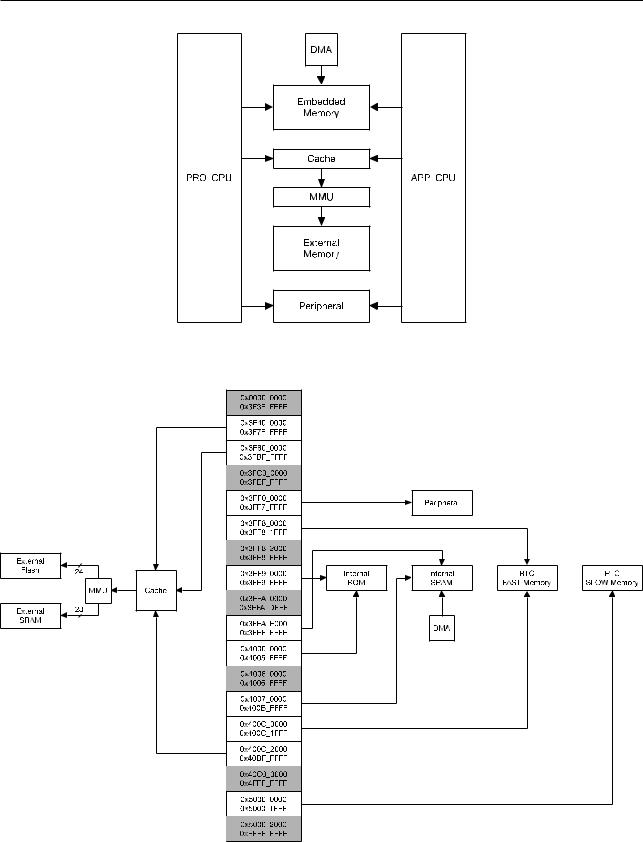
The ESP32 is a dual-core system with two Harvard Architecture Xtensa LX6 CPUs. All embedded memory, external memory and peripherals are located on the data bus and/or the instruction bus of these CPUs.
With some minor exceptions (see below), the address mapping of two CPUs is symmetric, meaning that they use the same addresses to access the same memory. Multiple peripherals in the system can access embedded memory via DMA.
The two CPUs are named “PRO_CPU” and “APP_CPU” (for “protocol” and “application”), however, for most purposes the two CPUs are interchangeable.
1.2Features
•Address Space
–Symmetric address mapping
–4 GB (32-bit) address space for both data bus and instruction bus
–1296 KB embedded memory address space
–19704 KB external memory address space
–512 KB peripheral address space
–Some embedded and external memory regions can be accessed by either data bus or instruction bus
–328 KB DMA address space
•Embedded Memory
–448 KB Internal ROM
–520 KB Internal SRAM
–8 KB RTC FAST Memory
–8 KB RTC SLOW Memory
•External Memory
Off-chip SPI memory can be mapped into the available address space as external memory. Parts of the embedded memory can be used as transparent cache for this external memory.
–Supports up to 16 MB off-Chip SPI Flash.
–Supports up to 8 MB off-Chip SPI SRAM.
•Peripherals
–41 peripherals
•DMA
–13 modules are capable of DMA operation
The block diagram in Figure 1-1 illustrates the system structure, and the block diagram in Figure 1-2 illustrates the address map structure.
Espressif Systems |
24 |
ESP32 TRM (Version 5.0) |
Submit Documentation Feedback
1 System and Memory
Figure 11. System Structure
Figure 12. System Address Mapping
Espressif Systems |
25 |
ESP32 TRM (Version 5.0) |
Submit Documentation Feedback