

2 Pins
2.3Power Supply
ESP32’s digital pins are divided into three different power domains:
•VDD3P3_RTC
•VDD3P3_CPU
•VDD_SDIO
VDD3P3_RTC is also the input power supply for RTC and CPU.
VDD3P3_CPU is also the input power supply for CPU.
VDD_SDIO connects to the output of an internal LDO whose input is VDD3P3_RTC. When VDD_SDIO is connected to the same PCB net together with VDD3P3_RTC, the internal LDO is disabled automatically.
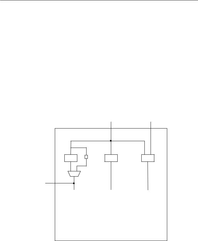
2.3.1Power Scheme
VDD3P3_RTC |
VDD3P3_CPU |
1.8 V LDO |
R = 6 Ω |
LDO 1.1 V |
LDO 1.1 V |
|
VDD_SDIO
3.3 V/1.8 V
SDIO |
|
RTC |
|
CPU |
Domain |
|
Domain |
|
Domain |
|
|
|
|
|
|
|
|
|
|
Figure 2-3. ESP32 Power Scheme
The internal LDO can be configured as having 1.8 V, or the same voltage as VDD3P3_RTC. It can be powered off via software to minimize the current of flash/SRAM during the Deep-sleep mode.
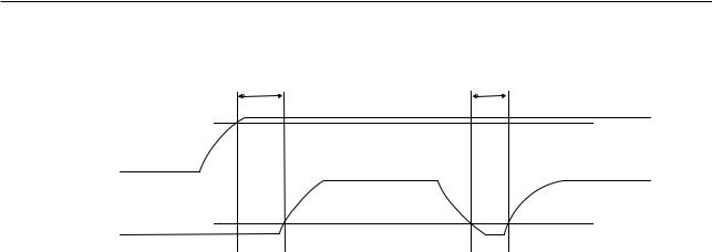
2.3.2Chip Power-up and Reset
Once the power is supplied to the chip, its power rails need a short time to stabilize. After that, CHIP_PU – the pin used for power-up and reset – is pulled high to activate the chip. For information on CHIP_PU as well as
Espressif Systems |
18 |
ESP32 Series Datasheet v4.3 |
Submit Documentation Feedback
2 Pins
power-up and reset timing, see Figure 2-4 and Table 2-2.
tSTBL |
tRST |
VDD3P3_RTC Min
VDD
VIL_nRST
CHIP_PU
Figure 2-4. Visualization of Timing Parameters for Power-up and Reset
Table 2-2. Description of Timing Parameters for Power-up and Reset
Parameter |
Description |
|
Min (µs) |
tSTBL |
Time reserved for the 3.3 V rails to stabilize before the CHIP_PU pin |
50 |
|
is pulled high to activate the chip |
|
||
|
|
|
|
|
|
|
|
tRST |
Time reserved for CHIP_PU to stay below VIL_nRST |
to reset the |
50 |
chip (see Table 4-3) |
|
||
|
|
|
|
|
|
|
|
•In scenarios where ESP32 is powered up and down repeatedly by switching the power rails, while there is a large capacitor on the VDD33 rail and CHIP_PU and VDD33 are connected, simply switching off the CHIP_PU power rail and immediately switching it back on may cause an incomplete power discharge cycle and failure to reset the chip adequately.
An additional discharge circuit may be required to accelerate the discharge of the large capacitor on rail VDD33, which will ensure proper power-on-reset when the ESP32 is powered up again.
•When a battery is used as the power supply for the ESP32 series of chips and modules, a supply voltage supervisor is recommended, so that a boot failure due to low voltage is avoided. Users are recommended to pull CHIP_PU low if the power supply for ESP32 is below 2.3 V.
Notes on power supply:
•The operating voltage of ESP32 ranges from 2.3 V to 3.6 V. When using a single-power supply, the recommended voltage of the power supply is 3.3 V, and its recommended output current is 500 mA or more.
•PSRAM and flash both are powered by VDD_SDIO. If the chip has an in-package flash, the voltage of VDD_SDIO is determined by the operating voltage of the in-package flash. If the chip also connects to an external PSRAM, the operating voltage of external PSRAM must match that of the in-package flash. This also applies if the chip has an in-package PSRAM but also connects to an external flash.
•When VDD_SDIO 1.8 V is used as the power supply for external flash/PSRAM, a 2 kΩ grounding resistor should be added to VDD_SDIO. For the circuit design, please refer to ESP32-WROVER Datasheet > Figure
Schematics of ESP32-WROVER.
•When the three digital power supplies are used to drive peripherals, e.g., 3.3 V flash, they should comply with the peripherals’ specifications.
Espressif Systems |
19 |
ESP32 Series Datasheet v4.3 |
Submit Documentation Feedback