

opa627[1]
.pdf®
 OPA627
 OPA627
OPA627
OPA637
Precision High-Speed
Difet ® OPERATIONAL AMPLIFIERS
FEATURES
●VERY LOW NOISE: 4.5nV/ÖHz at 10kHz
●FAST SETTLING TIME: OPA627—550ns to 0.01% OPA637—450ns to 0.01%
●LOW VOS: 100mV max
●LOW DRIFT: 0.8mV/°C max
●LOW IB: 5pA max
●OPA627: Unity-Gain Stable
●OPA637: Stable in Gain ³ 5
DESCRIPTION
The OPA627 and OPA637 Difet operational amplifiers provide a new level of performance in a precision FET op amp. When compared to the popular OPA111 op amp, the OPA627/637 has lower noise, lower offset voltage, and much higher speed. It is useful in a broad range of precision and high speed analog circuitry.
The OPA627/637 is fabricated on a high-speed, dielec- trically-isolated complementary NPN/PNP process. It operates over a wide range of power supply voltage—
±4.5V to ±18V. Laser-trimmed Difet input circuitry provides high accuracy and low-noise performance comparable with the best bipolar-input op amps.
APPLICATIONS
●PRECISION INSTRUMENTATION
●FAST DATA ACQUISITION
●DAC OUTPUT AMPLIFIER
●OPTOELECTRONICS
●SONAR, ULTRASOUND
●HIGH-IMPEDANCE SENSOR AMPS
●HIGH-PERFORMANCE AUDIO CIRCUITRY
●ACTIVE FILTERS
High frequency complementary transistors allow increased circuit bandwidth, attaining dynamic performance not possible with previous precision FET op amps. The OPA627 is unity-gain stable. The OPA637 is stable in gains equal to or greater than five.
Difet fabrication achieves extremely low input bias currents without compromising input voltage noise performance. Low input bias current is maintained over a wide input common-mode voltage range with unique cascode circuitry.
The OPA627/637 is available in plastic DIP, SOIC and metal TO-99 packages. Industrial and military temperature range models are available.
|
|
7 |
|
Trim |
Trim |
+VS |
|
1 |
5 |
||
|
|||
|
|
Output |
|
|
|
6 |
|
+In |
|
–In |
|
3 |
|
2 |
|
Difet ® , Burr-Brown Corp. |
|
–VS |
|
|
|
4 |
International Airport Industrial Park • Mailing Address: PO Box 11400, Tucson, AZ 85734 • Street Address: 6730 S. Tucson Blvd., Tucson, AZ 85706 • Tel: (520) 746-1111 • Twx: 910-952-1111 Internet: http://www.burr-brown.com/ • FAXLine: (800) 548-6133 (US/Canada Only) • Cable: BBRCORP • Telex: 066-6491 • FAX: (520) 889-1510 • Immediate Product Info: (800) 548-6132
©1989 Burr-Brown Corporation PDS-998H Printed in U.S.A. March, 1998
SBOS165

SPECIFICATIONS
ELECTRICAL
At TA = +25°C, and VS = ±15V, unless otherwise noted.
|
|
OPA627BM, BP, SM |
OPA627AM, AP, AU |
|
|
|
|
|
|
|
||||
|
|
OPA637BM, BP, SM |
OPA637AM, AP, AU |
|
|
|
|
|
|
|
||||
PARAMETER |
CONDITIONS |
MIN |
TYP |
MAX |
MIN |
TYP |
MAX |
UNITS |
||||||
|
|
|
|
|
|
|
|
|
|
|
|
|
|
|
OFFSET VOLTAGE (1) |
|
|
|
|
|
|
|
mV |
||||||
Input Offset Voltage |
|
|
40 |
100 |
|
130 |
250 |
|||||||
AP, BP, AU Grades |
|
|
100 |
250 |
|
280 |
500 |
mV |
||||||
Average Drift |
|
|
0.4 |
0.8 |
|
1.2 |
2 |
mV/°C |
||||||
AP, BP, AU Grades |
VS = ±4.5 to ±18V |
|
0.8 |
2 |
|
2.5 |
|
mV/°C |
||||||
Power Supply Rejection |
106 |
120 |
|
100 |
116 |
|
dB |
|||||||
|
|
|
|
|
|
|
|
|
|
|
|
|
|
|
INPUT BIAS CURRENT (2) |
|
|
|
|
|
|
|
|
|
|
|
|
|
|
Input Bias Current |
VCM = 0V |
|
1 |
5 |
|
2 |
10 |
pA |
||||||
Over Specified Temperature |
VCM = 0V |
|
|
1 |
|
|
2 |
nA |
||||||
SM Grade |
VCM = 0V |
|
|
50 |
|
|
|
nA |
||||||
Over Common-Mode Voltage |
VCM = ±10V |
|
1 |
|
|
2 |
|
pA |
||||||
Input Offset Current |
VCM = 0V |
|
0.5 |
5 |
|
1 |
10 |
pA |
||||||
Over Specified Temperature |
VCM = 0V |
|
|
1 |
|
|
2 |
nA |
||||||
SM Grade |
|
|
|
50 |
|
|
|
nA |
||||||
NOISE |
|
|
|
|
|
|
|
|
|
|
|
|
|
|
Input Voltage Noise |
|
|
|
|
|
|
|
nV/Ö |
|
|
|
|
|
|
Noise Density: f = 10Hz |
|
|
15 |
40 |
|
20 |
|
Hz |
|
|||||
f = 100Hz |
|
|
8 |
20 |
|
10 |
|
nV/Ö |
Hz |
|
||||
f = 1kHz |
|
|
5.2 |
8 |
|
5.6 |
|
nV/ÖHz |
||||||
f = 10kHz |
|
|
4.5 |
6 |
|
4.8 |
|
nV/ÖHz |
||||||
Voltage Noise, BW = 0.1Hz to 10Hz |
|
|
0.6 |
1.6 |
|
0.8 |
|
mVp-p |
||||||
Input Bias Current Noise |
|
|
|
|
|
|
|
|
|
|
|
|
|
|
Noise Density, f = 100Hz |
|
|
1.6 |
2.5 |
|
2.5 |
|
fA/Ö |
Hz |
|
|
|||
Current Noise, BW = 0.1Hz to 10Hz |
|
|
30 |
60 |
|
48 |
|
fAp-p |
||||||
|
|
|
|
|
|
|
|
|
|
|
|
|
|
|
INPUT IMPEDANCE |
|
|
|
|
|
|
|
W || pF |
||||||
Differential |
|
|
1013 || 8 |
|
|
* |
|
|||||||
Common-Mode |
|
|
1013 || 7 |
|
|
* |
|
W || pF |
||||||
INPUT VOLTAGE RANGE |
|
±11 |
±11.5 |
|
|
|
|
|
|
|
|
|
|
|
Common-Mode Input Range |
|
|
* |
* |
|
V |
||||||||
Over Specified Temperature |
VCM = ±10.5V |
±10.5 |
±11 |
|
* |
* |
|
V |
||||||
Common-Mode Rejection |
106 |
116 |
|
100 |
110 |
|
dB |
|||||||
OPEN-LOOP GAIN |
VO = ±10V, RL = 1kW |
|
|
|
|
|
|
|
|
|
|
|
|
|
Open-Loop Voltage Gain |
112 |
120 |
|
106 |
116 |
|
dB |
|||||||
Over Specified Temperature |
VO = ±10V, RL = 1kW |
106 |
117 |
|
100 |
110 |
|
dB |
||||||
SM Grade |
VO = ±10V, RL = 1kW |
100 |
114 |
|
|
|
|
dB |
||||||
FREQUENCY RESPONSE |
|
|
|
|
|
|
|
V/ms |
||||||
Slew Rate: OPA627 |
G = –1, 10V Step |
40 |
55 |
|
* |
* |
|
|||||||
OPA637 |
G = –4, 10V Step |
100 |
135 |
|
* |
* |
|
V/ms |
||||||
Settling Time: OPA627 0.01% |
G = –1, 10V Step |
|
550 |
|
|
* |
|
ns |
||||||
0.1% |
G = –1, 10V Step |
|
450 |
|
|
* |
|
ns |
||||||
OPA637 0.01% |
G = –4, 10V Step |
|
450 |
|
|
* |
|
ns |
||||||
0.1% |
G = –4, 10V Step |
|
300 |
|
|
* |
|
ns |
||||||
Gain-Bandwidth Product: OPA627 |
G = 1 |
|
16 |
|
|
* |
|
MHz |
||||||
OPA637 |
G = 10 |
|
80 |
|
|
* |
|
MHz |
||||||
Total Harmonic Distortion + Noise |
G = +1, f = 1kHz |
|
0.00003 |
|
|
* |
|
% |
|
|
|
|||
|
|
|
|
|
|
|
|
|
|
|
|
|
|
|
POWER SUPPLY |
|
|
±15 |
|
|
|
|
|
|
|
|
|
|
|
Specified Operating Voltage |
|
±4.5 |
±18 |
|
* |
|
V |
|||||||
Operating Voltage Range |
|
|
* |
|
* |
V |
||||||||
Current |
|
|
±7 |
±7.5 |
|
* |
* |
mA |
||||||
OUTPUT |
RL = 1kW |
±11.5 |
±12.3 |
|
|
|
|
|
|
|
|
|
|
|
Voltage Output |
|
* |
* |
|
|
|
|
|
|
|
|
|||
Over Specified Temperature |
|
±11 |
±11.5 |
|
* |
* |
|
V |
||||||
Current Output |
VO = ±10V |
±35 |
±45 |
±100 |
|
* |
|
mA |
||||||
Short-Circuit Current |
|
+70/–55 |
* |
* |
* |
mA |
||||||||
Output Impedance, Open-Loop |
1MHz |
|
55 |
|
|
* |
|
W |
||||||
|
|
|
|
|
|
|
|
|
|
|
|
|
|
|
TEMPERATURE RANGE |
|
|
|
|
|
|
|
°C |
||||||
Specification: AP, BP, AM, BM, AU |
|
–25 |
|
+85 |
* |
|
* |
|||||||
SM |
|
–55 |
|
+125 |
|
|
|
°C |
||||||
Storage: AM, BM, SM |
|
–60 |
|
+150 |
* |
|
* |
°C |
||||||
AP, BP, AU |
|
–40 |
|
+125 |
* |
|
* |
°C |
||||||
θJ-A: AM, BM, SM |
|
|
200 |
|
|
* |
|
°C/W |
||||||
AP, BP |
|
|
100 |
|
|
* |
|
°C/W |
||||||
AU |
|
|
160 |
|
|
|
|
°C/W |
||||||
|
|
|
|
|
|
|
|
|
|
|
|
|
|
|
* Specifications same as “B” grade.
NOTES: (1) Offset voltage measured fully warmed-up. (2) High-speed test at TJ = +25°C. See Typical Performance Curves for warmed-up performance.
The information provided herein is believed to be reliable; however, BURR-BROWN assumes no responsibility for inaccuracies or omissions. BURR-BROWN assumes no responsibility for the use of this information, and all use of such information shall be entirely at the user’s own risk. Prices and specifications are subject to change without notice. No patent rights or licenses to any of the circuits described herein are implied or granted to any third party. BURR-BROWN does not authorize or warrant any BURR-BROWN product for use in life support devices and/or systems.


 ®
®
|
OPA627, 637 |
2 |
|
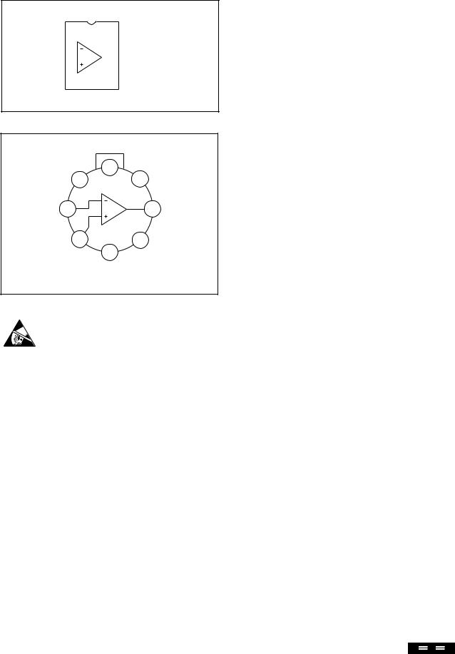
PIN CONFIGURATIONS
Top View DIP/SOIC
Offset Trim |
1 |
|
|
|
8 |
No Internal Connection |
|
–In |
|
|
|
|
|
|
|
|
|
|
|
|
|
||
2 |
|
|
|
7 |
+VS |
||
|
|
|
|
||||
+In |
|
|
|
|
|
|
|
3 |
|
|
|
|
6 |
Output |
|
|
|
|
|
||||
|
|
|
|
||||
–VS |
|
|
|
|
|
|
|
|
|
|
|
|
|
||
4 |
|
|
|
5 |
Offset Trim |
||
Top View |
|
TO-99 |
|
|
No Internal Connection |
||
Offset Trim |
8 |
+VS |
|
|
|||
1 |
7 |
||
|
|||
–In 2 |
|
6 Output |
|
|
3 |
5 |
|
+In |
4 |
Offset Trim |
|
–VS
Case connected to –VS.
ELECTROSTATIC DISCHARGE SENSITIVITY
This integrated circuit can be damaged by ESD. Burr-Brown recommends that all integrated circuits be handled with appropriate precautions. Failure to observe proper handling and installation procedures can cause damage.
ESD damage can range from subtle performance degradation to complete device failure. Precision integrated circuits may be more susceptible to damage because very small parametric changes could cause the device not to meet its published specifications.
ABSOLUTE MAXIMUM RATINGS(1)
..................................................................................Supply Voltage |
±18V |
Input Voltage Range .............................................. |
+VS + 2V to –VS – 2V |
Differential Input Range ....................................................... |
Total VS + 4V |
Power Dissipation ........................................................................ |
1000mW |
Operating Temperature |
–55°C to +125°C |
M Package .................................................................. |
|
P, U Package ............................................................. |
–40°C to +125°C |
Storage Temperature |
–65°C to +150°C |
M Package .................................................................. |
|
P, U Package ............................................................. |
–40°C to +125°C |
Junction Temperature |
+175°C |
M Package .................................................................................. |
|
P, U Package ............................................................................. |
+150°C |
Lead Temperature (soldering, 10s) ............................................... |
+300°C |
SOlC (soldering, 3s) ................................................................... |
+260°C |
NOTE: (1) Stresses above these ratings may cause permanent damage.
PACKAGE/ORDERING INFORMATION
|
|
PACKAGE DRAWING |
TEMPERATURE |
PRODUCT |
PACKAGE |
NUMBER(1) |
RANGE |
OPA627AP |
Plastic DIP |
006 |
–25°C to +85°C |
OPA627BP |
Plastic DIP |
006 |
–25°C to +85°C |
OPA627AU |
SOIC |
182 |
–25°C to +85°C |
OPA627AM |
TO-99 Metal |
001 |
–25°C to +85°C |
OPA627BM |
TO-99 Metal |
001 |
–25°C to +85°C |
OPA627SM |
TO-99 Metal |
001 |
–55°C to +125°C |
OPA637AP |
Plastic DIP |
006 |
–25°C to +85°C |
OPA637BP |
Plastic DIP |
006 |
–25°C to +85°C |
OPA637AU |
SOIC |
182 |
–25°C to +85°C |
OPA637AM |
TO-99 Metal |
001 |
–25°C to +85°C |
OPA637BM |
TO-99 Metal |
001 |
–25°C to +85°C |
OPA637SM |
TO-99 Metal |
001 |
–55°C to +125°C |
NOTE: (1) For detailed drawing and dimension table, please see end of data sheet, or Appendix C of Burr-Brown IC Data Book.


 ®
®
3 |
OPA627, 637 |
|
|
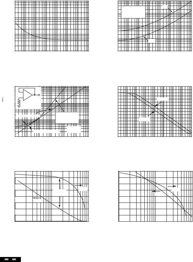
TYPICAL PERFORMANCE CURVES
At TA = +25°C, and VS = ±15V, unless otherwise noted.
INPUT VOLTAGE NOISE SPECTRAL DENSITY
|
|
1k |
|
Hz) |
|
|
|
|
|
Ö |
100 |
|
Noise (nV/ |
|
|
|
|
|
Voltage |
10 |
|
|
1 |
1 |
10 |
100 |
1k |
10k |
100k |
1M |
10M |
Frequency (Hz)
VOLTAGE NOISE vs SOURCE RESISTANCE
|
1k |
|
|
|
|
|
|
|
|
– |
|
|
|
|
|
Hz) |
|
+ |
|
|
|
|
|
|
RS |
|
|
|
|
|
|
Ö |
100 |
|
|
|
|
|
|
(nV/ |
|
|
|
|
|
|
|
|
|
|
|
|
|
|
|
Noise |
OPA627 + Resistor |
|
Comparison with |
|
|||
|
OPA27 Bipolar Op |
|
|||||
Voltage |
|
|
|||||
10 |
|
|
|
|
|||
|
|
|
Amp + Resistor |
|
|||
|
|
|
|
|
|||
|
|
|
|
|
Spot Noise |
|
|
|
|
|
|
|
|
|
|
|
|
|
Resistor Noise Only |
at 10kHz |
|
||
|
1 |
1k |
10k |
100k |
1M |
10M |
100M |
|
100 |
||||||
|
|
|
Source Resistance (Ω) |
|
|
||
TOTAL INPUT VOLTAGE NOISE vs BANDWIDTH
|
100 |
|
|
|
|
|
|
|
|
|
Noise Bandwidth: |
|
|
p-p |
|
|
|
|
|
|
|
|
|
|
||
(µV) |
10 |
0.1Hz to indicated |
|
|
|
|
|
|
frequency. |
|
|
|
|
|
|
||
|
|
|
|
|
|
|
||
Noise |
|
|
|
|
|
|
|
|
|
|
|
|
|
|
|
|
|
Voltage |
1 |
|
|
|
|
|
|
|
|
|
|
|
|
|
|
|
|
Input |
0.1 |
|
|
RMS |
|
|
|
|
|
|
|
|
|
|
|
||
|
|
|
|
|
|
|
|
|
|
0.01 |
|
|
|
|
|
|
|
|
1 |
10 |
100 |
1k |
10k |
100k |
1M |
10M |
Bandwidth (Hz)
OPEN-LOOP GAIN vs FREQUENCY
|
140 |
|
|
|
|
|
|
|
|
|
120 |
|
|
|
|
|
|
|
|
(dB) |
100 |
|
|
|
|
OPA637 |
|
|
|
80 |
|
|
|
|
|
|
|
|
|
Gain |
|
|
|
|
|
|
|
|
|
60 |
|
|
|
|
|
|
|
|
|
Voltage |
|
|
|
|
|
|
|
|
|
40 |
|
|
OPA627 |
|
|
|
|
|
|
|
|
|
|
|
|
|
|
||
20 |
|
|
|
|
|
|
|
|
|
|
|
|
|
|
|
|
|
|
|
|
0 |
|
|
|
|
|
|
|
|
|
–20 |
|
|
|
|
|
|
|
|
|
1 |
10 |
100 |
1k |
10k |
100k |
1M |
10M |
100M |
Frequency (Hz)
OPA627 GAIN/PHASE vs FREQUENCY |
OPA637 GAIN/PHASE vs FREQUENCY |
30 |
|
|
–90 |
|
30 |
20 |
|
|
–120 |
Phase (Degrees) |
20 |
|
|
75° Phase |
Phase |
|
|
|
|
|
|
||
10 |
|
Margin |
–150 |
10 |
|
|
|
||||
Gain(dB) |
Gain |
|
|
Gain(dB) |
|
|
|
|
|||
0 |
|
|
–180 |
|
0 |
–10 |
|
|
–210 |
|
–10 |
1 |
10 |
|
100 |
|
|
|
|
–90 |
|
|
|
–120 |
(Degrees) |
Gain |
Phase |
|
|
|
|
|
|
|
|
–150 |
Phase |
|
|
|
|
|
|
–180 |
|
–210
1 |
10 |
100 |
Frequency (MHz) |
Frequency (MHz) |


 ®
®
|
OPA627, 637 |
4 |
|
TYPICAL PERFORMANCE CURVES (CONT)
At TA = +25°C, and VS = ±15V, unless otherwise noted.
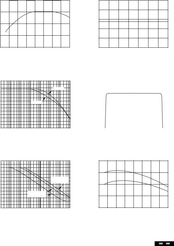
OPEN-LOOP GAIN vs TEMPERATURE
|
125 |
Gain (dB) |
120 |
115 |
|
Voltage |
110 |
|
105
–75 |
–50 |
–25 |
0 |
25 |
50 |
75 |
100 |
125 |
|
|
|
Temperature (°C) |
|
|
|
||
COMMON-MODE REJECTION vs FREQUENCY
(dB) |
140 |
|
|
120 |
OPA637 |
||
Ratio |
|||
|
|||
100 |
|
||
Rejection |
|
||
80 |
OPA627 |
||
|
|||
|
|
||
-Mode |
60 |
|
|
40 |
|
||
Common |
|
||
20 |
|
||
|
0 |
|
1 |
10 |
100 |
1k |
10k |
100k |
1M |
10M |
|
|
|
Frequency (Hz) |
|
|
|
|
OPEN-LOOP OUTPUT IMPEDANCE vs FREQUENCY
|
100 |
) |
80 |
(Ω |
|
Resistance |
60 |
|
|
Output |
40 |
|
|
|
20 |
|
0 |
2 |
20 |
200 |
2k |
20k |
200k |
2M |
20M |
|
|
|
Frequency (Hz) |
|
|
|
|
COMMON-MODE REJECTION vs
INPUT COMMON MODE VOLTAGE
(dB) |
130 |
|
|
|
|
|
|
|
|
|
|
|
|
|
|
|
|
|
|
|
|
|
|
|
|
|
|
|
|
|
|
|
120 |
|
|
|
|
|
|
|
|
|
|
|
|
|
|
|
|
|
|
|
|
|
|
|
|
|
|
|
|
|
|
|
|
|
|
|
|
|
|
|
|
|
|
|
|
|
|
|
|
|
|
|
|
|
|
|
|
|
|
|
|
|
|
|
||
|
|
|
|
|
|
|
|
|
|
|
|
|
|
|
|
|
|
|
|
|
|
|
|
|
|
|
|
|
|
|
||
Mode Rejection |
|
|
|
|
|
|
|
|
|
|
|
|
|
|
|
|
|
|
|
|
|
|
|
|
|
|
|
|
|
|
|
|
110 |
|
|
|
|
|
|
|
|
|
|
|
|
|
|
|
|
|
|
|
|
|
|
|
|
|
|
|
|
|
|
|
|
|
|
|
|
|
|
|
|
|
|
|
|
|
|
|
|
|
|
|
|
|
|
|
|
|
|
|
|
|
|
|
||
|
|
|
|
|
|
|
|
|
|
|
|
|
|
|
|
|
|
|
|
|
|
|
|
|
|
|
|
|
|
|
||
100 |
|
|
|
|
|
|
|
|
|
|
|
|
|
|
|
|
|
|
|
|
|
|
|
|
|
|
|
|
|
|
|
|
|
|
|
|
|
|
|
|
|
|
|
|
|
|
|
|
|
|
|
|
|
|
|
|
|
|
|
|
|
|
|
||
|
|
|
|
|
|
|
|
|
|
|
|
|
|
|
|
|
|
|
|
|
|
|
|
|
|
|
|
|
|
|
||
- |
|
|
|
|
|
|
|
|
|
|
|
|
|
|
|
|
|
|
|
|
|
|
|
|
|
|
|
|
|
|
|
|
Common |
90 |
|
|
|
|
|
|
|
|
|
|
|
|
|
|
|
|
|
|
|
|
|
|
|
|
|
|
|
|
|
|
|
|
|
|
|
|
|
|
|
|
|
|
|
|
|
|
|
|
|
|
|
|
|
|
|
|
|
|
|
|
|
|
||
|
|
|
|
|
|
|
|
|
|
|
|
|
|
|
|
|
|
|
|
|
|
|
|
|
|
|
|
|
|
|
||
|
|
|
|
|
|
|
|
|
|
|
|
|
|
|
|
|
|
|
|
|
|
|
|
|
|
|
|
|
|
|
|
|
|
80 |
|
|
|
|
|
|
|
|
|
|
|
|
|
|
|
|
|
|
|
|
|
|
|
|
|
|
|
|
|
|
|
|
|
|
|
|
|
|
|
|
|
|
|
|
|
|
|
|
|
|
|
|
|
|
|
|
|
|
|
|
|
|
|
|
|
|
|
|
|
|
|
|
|
|
|
|
|
|
|
|
|
|
|
|
|
|
|
|
|
|
|
|
|
|
|
|
|
|
–15 |
–10 |
–5 |
0 |
|
|
|
5 |
|
|
|
10 |
|
|
|
15 |
||||||||||||||||
Common-Mode Voltage (V)
Power-Supply Rejection (dB)
|
POWER-SUPPLY REJECTION vs FREQUENCY |
|
|||||
140 |
|
|
|
|
|
|
|
120 |
|
|
|
|
|
|
|
100 |
|
|
|
|
|
|
|
80 |
|
|
|
|
–VS PSRR 627 |
||
|
|
|
|
|
and 637 |
|
|
60 |
|
|
|
|
|
|
|
40 |
|
|
+VS PSRR 627 |
|
|
|
|
|
|
|
637 |
|
|
|
|
|
|
|
|
|
|
|
|
20 |
|
|
|
|
|
|
|
0 |
|
|
|
|
|
|
|
1 |
10 |
100 |
1k |
10k |
100k |
1M |
10M |
|
|
|
Frequency (Hz) |
|
|
|
|
CMR and PSR (dB)
POWER-SUPPLY REJECTION AND COMMON-MODE REJECTION vs TEMPERATURE
125
PSR
120
CMR
115
110
105
–75 |
–50 |
–25 |
0 |
25 |
50 |
75 |
100 |
125 |
Temperature (°C)


 ®
®
5 |
OPA627, 637 |
|
|

TYPICAL PERFORMANCE CURVES (CONT)
At TA = +25°C, and VS = ±15V, unless otherwise noted.
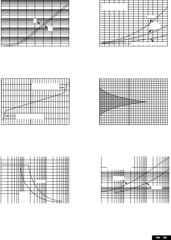
Supply Current (mA)
SUPPLY CURRENT vs TEMPERATURE |
OUTPUT CURRENT LIMIT vs TEMPERATURE |
8
7.5
7
6.5
6
–75 |
–50 |
–25 |
0 |
25 |
50 |
75 |
100 |
125 |
|
|
|
Temperature (°C) |
|
|
|
||
|
100 |
|
|
|
80 |
+IL at VO = 0V |
|
|
|
|
|
(mA) |
|
+IL at VO = +10V |
|
60 |
|
|
|
Current |
|
|
|
40 |
|
|
|
Output |
|
|
|
|
–IL at VO = 0V |
|
|
20 |
|
|
|
|
–IL at VO |
= –10V |
|
|
|
||
0
–75 |
–50 |
–25 |
0 |
25 |
50 |
75 |
100 |
125 |
|
|
|
Temperature (°C) |
|
|
|
||
OPA627 GAIN-BANDWIDTH AND SLEW RATE vs TEMPERATURE
|
24 |
|
|
|
|
|
|
|
60 |
Gain-Bandwidth (MHz) |
20 |
|
|
|
|
|
|
|
|
|
|
|
|
|
Slew Rate |
|
|
|
|
16 |
|
|
|
|
|
|
|
55 |
|
12 |
|
|
|
GBW |
|
|
Slew Rate(V/µs) |
||
|
|
|
|
|
|
|
|||
|
8 |
|
|
|
|
|
|
|
50 |
|
–75 |
–50 |
–25 |
0 |
25 |
50 |
75 |
100 |
125 |
Temperature (°C)
OPA637 GAIN-BANDWIDTH AND SLEW RATE vs TEMPERATURE
120 |
|
|
160 |
|
|
||
|
|
|
|
Slew Rate
Gain-Bandwidth(MHz) |
100 |
|
140 |
80 |
GBW |
120 |
|
|
Slew Rate(V/µs) |
||
60 |
|
||
|
|
100 |
40 |
|
|
|
|
|
|
|
|
|
80 |
|
|
|
|
|
|
|
|
|
||
–75 |
–50 |
–25 |
0 |
25 |
50 |
75 |
100 |
125 |
||
|
|
|
|
Temperature (°C) |
|
|
|
|
||
OPA627 TOTAL HARMONIC DISTORTION + NOISE vs FREQUENCY
|
0.1 |
G = +1 |
|
|
G = +10 |
|
|
|
|
|
|
||
|
VI |
+ |
VO = ±10V |
VI |
+ |
VO = ±10V |
|
|
– |
600 Ω |
|
– |
600 Ω |
|
|
|
100pF |
5kΩ |
||
|
0.01 |
|
|
100pF |
||
|
|
|
|
549Ω |
|
|
|
|
|
|
|
|
|
(%) |
|
|
|
|
|
|
THD+N |
0.001 |
Measurement BW: 80kHz |
|
|||
|
|
|
|
|
G = +10 |
|
|
|
|
|
|
|
|
|
0.0001 |
|
|
|
|
|
|
|
|
|
|
|
G = +1 |
0.00001
20 |
100 |
1k |
10k |
20k |
Frequency (Hz)
OPA637 TOTAL HARMONIC DISTORTION + NOISE vs FREQUENCY
|
1 |
G = +10 |
|
|
|
G = +50 |
|
|
|
|
|
|
|
|
|
||
|
VI |
+ |
|
VO = ±10V |
VI |
+ |
VO = ±10V |
|
|
|
– |
|
600Ω |
|
– |
600Ω |
|
|
0.1 |
|
5kΩ |
|
5kΩ |
|
||
|
|
|
100pF |
100pF |
|
|||
(%) |
|
549Ω |
|
|
|
102Ω |
|
|
0.01 |
|
|
|
|
|
|
|
|
THD+N |
|
|
|
|
G = +50 |
|
||
|
|
|
|
|
|
|||
|
Measurement BW: 80kHz |
|
|
|
||||
|
|
|
|
|
|
|
|
|
|
0.001 |
|
|
|
|
|
|
|
|
0.0001 |
|
|
|
|
|
G = +10 |
|
|
|
|
|
|
|
|
|
|
|
20 |
|
100 |
|
|
1k |
10k |
20k |
Frequency (Hz)


 ®
®
|
OPA627, 637 |
6 |
|
TYPICAL PERFORMANCE CURVES
At TA = +25°C, and VS = ±15V, unless otherwise noted.
INPUT BIAS AND OFFSET CURRENT vs JUNCTION TEMPERATURE
|
10k |
|
|
|
|
|
|
|
|
|
1k |
|
|
|
|
|
|
|
|
(pA) |
100 |
|
|
|
|
|
|
|
|
Current |
|
|
|
IB |
|
|
|
|
|
|
|
|
|
|
|
|
|
||
10 |
|
|
|
|
|
|
|
|
|
Input |
|
|
|
|
|
IOS |
|
|
|
|
|
|
|
|
|
|
|
||
|
1 |
|
|
|
|
|
|
|
|
|
0.1 |
|
|
|
|
|
|
|
|
|
–50 |
–25 |
0 |
25 |
50 |
75 |
100 |
125 |
150 |
Junction Temperature (°C)
INPUT BIAS CURRENT vs COMMON-MODE VOLTAGE
|
1.2 |
|
|
|
|
|
|
Multiplier |
|
|
|
Beyond Linear |
|
|
|
1.1 |
|
|
Common-Mode Range |
|
|||
|
|
|
|
|
|
||
|
|
|
|
|
|
|
|
Bias Current |
1 |
|
|
|
|
|
|
|
|
|
|
|
|
|
|
Input |
0.9 |
|
Beyond Linear |
|
|
|
|
|
|
|
|
|
|||
|
|
Common-Mode Range |
|
|
|
||
|
|
|
|
|
|
||
|
0.8 |
|
|
|
|
|
|
|
–15 |
–10 |
–5 |
0 |
5 |
10 |
15 |
|
|
|
Common-Mode Voltage (V) |
|
|
||
(CONT)
|
|
INPUT BIAS CURRENT |
|
|
vs POWER SUPPLY VOLTAGE |
|
20 |
|
|
|
NOTE: Measured fully |
(pA) |
|
warmed-up. |
15 |
|
|
Current |
|
|
|
TO-99 |
|
|
|
|
Bias |
10 |
Plastic |
|
||
|
DIP, SOIC |
|
Input |
5 |
|
|
|
|
|
|
TO-99 with 0807HS Heat Sink |
0
±4 |
±6 |
±8 |
±10 |
±12 |
±14 |
±16 |
±18 |
Supply Voltage (±VS)
INPUT OFFSET VOLTAGE WARM-UP vs TIME
|
50 |
|
(µV) |
25 |
|
Change |
||
|
||
Voltage |
0 |
|
|
||
Offset |
–25 |
|
|
||
|
–50 |
0 |
1 |
2 |
3 |
4 |
5 |
6 |
|
|
Time From Power Turn-On (Min) |
|
|
||
Output Voltage (Vp-p)
|
MAX OUTPUT VOLTAGE vs FREQUENCY |
|
|
SETTLING TIME vs CLOSED-LOOP GAIN |
|
|||||||||
30 |
|
100 |
|
|
|
|
|
|
|
|
|
|
|
|
|
|
|
|
|
|
|
|
|
|
|
|
|
|
|
|
|
|
|
|
|
|
|
|
|
|
|
|
|
|
|
|
(µs) |
|
Error Band: ±0.01% |
20 |
|
10 |
|
|
|
Time |
|
||
|
|
|
OPA627 |
|
|
|
|
|
|
|
OPA637 |
Settling |
|
|
10 |
|
1 |
OPA637 |
|
|
|
|||
|
OPA627 |
|
|
|
0 |
|
|
|
|
|
|
|
|
0.1 |
|
|
|
|
|
|
|
|
|
|
|
|
|
|
|
|
|
|
||
|
|
|
|
|
|
|
|
|
|
|
|
|
||
|
|
|
|
|
|
|
|
|
|
|
|
|
||
100k |
1M |
10M |
100M |
–1 |
–10 |
–100 |
–1000 |
|||||||
|
|
|
|
|
|
Frequency (Hz) |
|
|
|
|
Closed-Loop Gain (V/V) |
|
|
|


 ®
®
7 |
OPA627, 637 |
|
|
TYPICAL PERFORMANCE CURVES (CONT)
At TA = +25°C, and VS = ±15V, unless otherwise noted.
|
|
SETTLING TIME vs ERROR BAND |
|
||
|
1500 |
CF |
|
|
|
|
|
|
|
|
|
|
|
RI |
+5V |
OPA627 |
OPA637 |
|
|
RF |
RI 2kΩ |
500Ω |
|
|
|
– |
|||
(ns) |
1000 |
|
–5V |
RF 2kΩ |
2kΩ |
+ |
2kΩ |
||||
|
|
CF 6pF |
4pF |
||
Time |
|
|
|||
|
|
|
|||
|
|
|
|
|
|
Settling |
500 |
|
|
|
OPA627 |
|
|
|
G = –1 |
||
|
|
|
|
||
|
|
|
|
|
|
|
|
OPA637 |
|
|
|
|
|
G = –4 |
|
|
|
0 |
|
|
|
|
|
|
|
|
|
|
|
|
|
|
|
|
|
|
|
|
|
|
|
|
|
0.001 |
|
|
|
|
0.01 |
0.1 |
1 |
10 |
||||
|
|
|
|
|
|
|
|
|
Error Band (%) |
|
|
|
Settling Time (µs)
|
SETTLING TIME vs LOAD CAPACITANCE |
|
|||
3 |
|
|
|
|
|
|
|
|
OPA637 |
|
|
2 |
Error Band: |
|
G = –4 |
|
|
±0.01% |
|
|
|
|
|
|
|
|
|
|
|
1 |
|
|
OPA627 |
|
|
|
|
G = –1 |
|
|
|
0 |
|
|
|
|
|
0 |
150 |
200 |
300 |
400 |
500 |
|
|
Load Capacitance (pF) |
|
|
|
APPLICATIONS INFORMATION
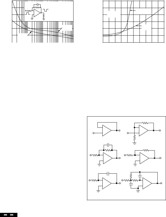
The OPA627 is unity-gain stable. The OPA637 may be used to achieve higher speed and bandwidth in circuits with noise gain greater than five. Noise gain refers to the closed-loop gain of a circuit as if the non-inverting op amp input were being driven. For example, the OPA637 may be used in a non-inverting amplifier with gain greater than five, or an inverting amplifier of gain greater than four.
When choosing between the OPA627 or OPA637, it is important to consider the high frequency noise gain of your circuit configuration. Circuits with a feedback capacitor (Figure 1) place the op amp in unity noise-gain at high frequency. These applications must use the OPA627 for proper stability. An exception is the circuit in Figure 2, where a small feedback capacitance is used to compensate for the input capacitance at the op amp’s inverting input. In this case, the closed-loop noise gain remains constant with frequency, so if the closed-loop gain is equal to five or greater, the OPA637 may be used.
|
|
|
RF < 4RI |
|
– |
OPA627 |
|
– |
OPA627 |
|
|
|
||
+ |
Buffer |
|
+ |
|
|
|
|
Non-Inverting Amp |
|
|
|
RI |
|
|
|
|
|
G < 5 |
|
|
|
|
|
RF < 4R |
– |
OPA627 |
RI |
– |
OPA627 |
|
|
|||
|
|
|
||
+ |
Bandwidth |
|
+ |
Inverting Amp |
|
|
|
||
|
Limiting |
|
|
G < |–4| |
– |
OPA627 |
|
|
OPA627 |
|
|
|
– |
|
+ |
Integrator |
|
|
+ |
|
|
|
Filter |
|
FIGURE 1. Circuits with Noise Gain Less than Five Require the OPA627 for Proper Stability.


 ®
®
|
OPA627, 637 |
8 |
|
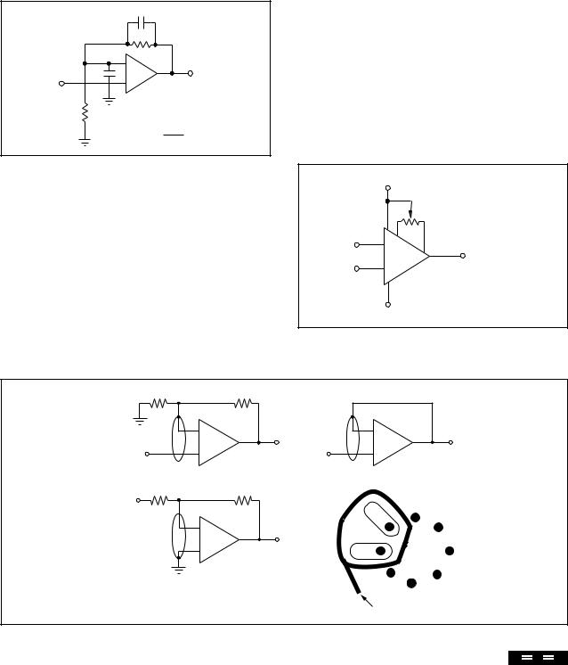
OFFSET VOLTAGE ADJUSTMENT
The OPA627/637 is laser-trimmed for low offset voltage and drift, so many circuits will not require external adjustment. Figure 3 shows the optional connection of an external potentiometer to adjust offset voltage. This adjustment should not be used to compensate for offsets created elsewhere in a system (such as in later amplification stages or in an A/D converter) because this could introduce excessive temperature drift. Generally, the offset drift will change by approximately 4μV/°C for 1mV of change in the offset voltage due to an offset adjustment (as shown on Figure 3).
|
|
C2 |
C1 |
– |
R2 |
|
|
|
|
+ |
OPA637 |
|
|
|
R1 |
|
C1 = CIN + CSTRAY |
C2 = R1 C1
R2
FIGURE 2. Circuits with Noise Gain Equal to or Greater than Five May Use the OPA637.
NOISE PERFORMANCE
Some bipolar op amps may provide lower voltage noise performance, but both voltage noise and bias current noise contribute to the total noise of a system. The OPA627/637 is unique in providing very low voltage noise and very low current noise. This provides optimum noise performance over a wide range of sources, including reactive source impedances. This can be seen in the performance curve showing the noise of a source resistor combined with the noise of an OPA627. Above a 2kΩ source resistance, the op
amp contributes little additional noise. Below 1kΩ, op amp noise dominates over the resistor noise, but compares favorably with precision bipolar op amps.
CIRCUIT LAYOUT
As with any high speed, wide bandwidth circuit, careful layout will ensure best performance. Make short, direct interconnections and avoid stray wiring capacitance—espe- cially at the input pins and feedback circuitry.
The case (TO-99 metal package only) is internally connected to the negative power supply as it is with most common op amps. Pin 8 of the plastic DIP, SOIC, and TO-99 packages has no internal connection.
Power supply connections should be bypassed with good high frequency capacitors positioned close to the op amp pins. In most cases 0.1μF ceramic capacitors are adequate. The OPA627/637 is capable of high output current (in excess of 45mA). Applications with low impedance loads or capacitive loads with fast transient signals demand large currents from the power supplies. Larger bypass capacitors such as 1μF solid tantalum capacitors may improve dynamic performance in these applications.
+VS |
|
|
|
100kΩ |
10kΩ to 1MΩ |
7 |
|
|
1 |
|
Potentiometer |
2 |
5 |
(100kΩ preferred) |
– |
||
3 + |
6 |
|
OPA627/637
4
±10mV Typical
Trim Range
–VS
FIGURE 3. Optional Offset Voltage Trim Circuit.
|
Non-inverting |
|
|
|
Buffer |
|
|
2 |
– |
|
|
2 |
– |
|
|
6 |
Out |
|
|
6 |
|
3 |
|
|
3 |
Out |
|
In |
+ |
|
In |
+ |
||
|
|
OPA627 |
|
|
|
OPA627 |
|
|
|
|
|
|
|
Inverting |
|
TO-99 Bottom View |
|
|
|
|
|
In |
|
|
|
OPA627 |
3 |
4 |
|
2 – |
|
5 |
|
|
|
||
6 |
Out |
|
|
3 + |
|
|
|
2 |
|
6 |
|
Board Layout for Input Guarding: |
|
|
|
Guard top and bottom of board. |
|
|
7 |
Alternate—use Teflon® standoff for sen- |
|
1 |
|
|
No Internal Connection |
||
sitive input pins. |
|
8 |
|
|
|
|
|
Teflon® E.I. du Pont de Nemours & Co. |
To Guard Drive |
|
FIGURE 4. Connection of Input Guard for Lowest IB.


 ®
®
9 |
OPA627, 637 |
|
|
INPUT BIAS CURRENT
Difet fabrication of the OPA627/637 provides very low input bias current. Since the gate current of a FET doubles approximately every 10°C, to achieve lowest input bias current, the die temperature should be kept as low as possible. The high speed and therefore higher quiescent current of the OPA627/637 can lead to higher chip temperature. A simple press-on heat sink such as the Burr-Brown model 807HS (TO-99 metal package) can reduce chip temperature by approximately 15°C, lowering the IB to one-third its warmed-up value. The 807HS heat sink can also reduce lowfrequency voltage noise caused by air currents and thermoelectric effects. See the data sheet on the 807HS for details.
Temperature rise in the plastic DIP and SOIC packages can be minimized by soldering the device to the circuit board. Wide copper traces will also help dissipate heat.
The OPA627/637 may also be operated at reduced power supply voltage to minimize power dissipation and tempera-
ture rise. Using ±5V power supplies reduces power dissipation to one-third of that at ±15V. This reduces the IB of TO-
99 metal package devices to approximately one-fourth the value at ±15V.
Leakage currents between printed circuit board traces can easily exceed the input bias current of the OPA627/637. A circuit board “guard” pattern (Figure 4) reduces leakage effects. By surrounding critical high impedance input circuitry with a low impedance circuit connection at the same potential, leakage current will flow harmlessly to the lowimpedance node. The case (TO-99 metal package only) is
internally connected to –V.
S
Input bias current may also be degraded by improper handling or cleaning. Contamination from handling parts and circuit boards may be removed with cleaning solvents and
deionized water. Each rinsing operation should be followed by a 30-minute bake at 85°C.
Many FET-input op amps exhibit large changes in input bias current with changes in input voltage. Input stage cascode circuitry makes the input bias current of the OPA627/637 virtually constant with wide common-mode voltage changes. This is ideal for accurate high inputimpedance buffer applications.
PHASE-REVERSAL PROTECTION
The OPA627/637 has internal phase-reversal protection. Many FET-input op amps exhibit a phase reversal when the input is driven beyond its linear common-mode range. This is most often encountered in non-inverting circuits when the input is driven below –12V, causing the output to reverse into the positive rail. The input circuitry of the OPA627/637 does not induce phase reversal with excessive commonmode voltage, so the output limits into the appropriate rail.
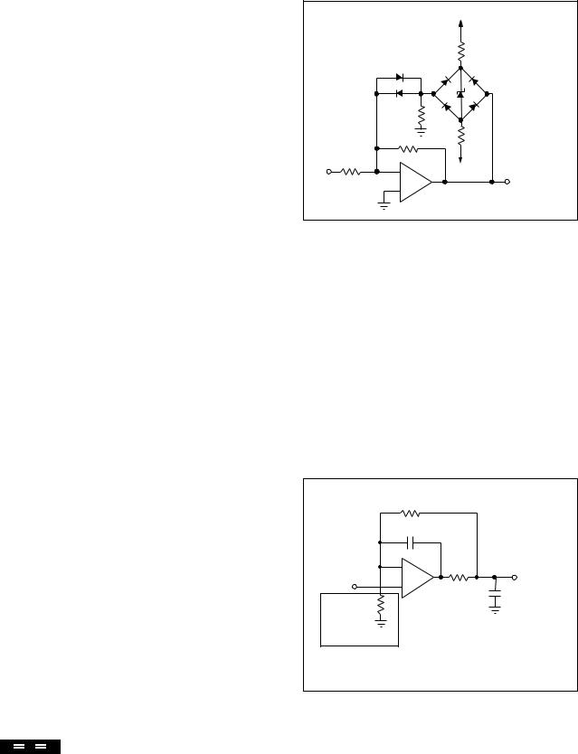
OUTPUT OVERLOAD
When the inputs to the OPA627/637 are overdriven, the output voltage of the OPA627/637 smoothly limits at approximately 2.5V from the positive and negative power supplies. If driven to the negative swing limit, recovery


 ®
®
takes approximately 500ns. When the output is driven into the positive limit, recovery takes approximately 6μs. Output recovery of the OPA627 can be improved using the output clamp circuit shown in Figure 5. Diodes at the inverting input prevent degradation of input bias current.
|
|
+VS |
|
|
(2) |
5kW |
|
|
|
|
|
|
HP 5082-2811 |
|
|
|
|
ZD1 |
Diode Bridge |
|
|
|
BB: PWS740-3 |
|
1kW |
|
|
|
|
5kW |
ZD1 : 10V IN961 |
|
RF |
|
|
VI |
– |
–VS |
VO |
|
RI |
|
|
|
+ |
Clamps output |
|
|
OPA627 |
||
at VO = ±11.5V
FIGURE 5. Clamp Circuit for Improved Overload Recovery.
CAPACITIVE LOADS
As with any high-speed op amp, best dynamic performance can be achieved by minimizing the capacitive load. Since a load capacitance presents a decreasing impedance at higher frequency, a load capacitance which is easily driven by a slow op amp can cause a high-speed op amp to perform poorly. See the typical curves showing settling times as a function of capacitive load. The lower bandwidth of the OPA627 makes it the better choice for driving large capacitive loads. Figure 6 shows a circuit for driving very large load capacitance. This circuit’s two-pole response can also be used to sharply limit system bandwidth. This is often useful in reducing the noise of systems which do not require the full bandwidth of the OPA627.
RF 1kW
|
|
|
200pF |
|
|
|
|
|
|
|
|
|
|
|
CF |
|
|
RO |
|
|
G = +1 |
||
|
|
|
|
|
|
|
BW ³ 1MHz |
||||
|
|
|
|
|
|
|
|
||||
|
|
|
– |
|
|
20W |
|
|
|
||
|
RF |
+ |
|
|
|
|
|
|
|
CL |
|
|
OPA627 |
|
5nF |
||||||||
G = 1+ |
|
|
R1 |
|
|
|
|
|
|
|
|
R1 |
|
|
|
|
|
|
|
|
|||
|
|
|
|
|
|
|
|
|
|
||
Optional Gain |
For Approximate Butterworth Response: |
||||||||||
|
2 RO CL |
|
|
|
|||||||
Gain > 1 |
CF = |
RF |
>> RO |
||||||||
|
|
|
|
RF |
|
||||||
|
|
|
|
|
|
|
|
||||
|
|
|
f–3dB |
= |
|
|
|
1 |
|
|
|
|
|
|
|
|
|
|
|
|
|||
|
|
|
|
|
|
|
|
|
|||
|
|
|
2p Ö RF RO CF CL |
||||||||
|
|
|
|
|
|
||||||
FIGURE 6. Driving Large Capacitive Loads.
|
OPA627, 637 |
10 |
|